 | –≠–ª–µ–∫—Ç—Ä–æ–Ω–Ω—ã–π –∫–æ–º–ø–æ–Ω–µ–Ω—Ç: UPS530 | –°–∫–∞—á–∞—Ç—å:  PDF PDF  ZIP ZIP |
Microsemi
Microsemi Integrated Products
11861 Western Avenue, Garden Grove, CA. 92841, 714-898-8121, Fax: 714-893-2570
Page 1
Copyright
©
2002
Rev. 3.0a, 2005-03-14
WWW
.
Microse
m
i
.
CO
M
LX1734
1.0MHz Inverting DC/DC Converter
TM
Æ
D E S C R I P T I O N
The LX1734 is an inverting
DC/DC current-mode controller. With
a 750mA integrated switch, the
LX1734 can generate large output
currents in a small footprint. The
LX1734 minimizes external com-
ponent size and cost by implementing
a high switching frequency of
1.0MHz, while generating -5V at
250mA.
When configured in the dual
inductor inverting topology very low
output voltage ripple approaching
1mV
P-P
can be achieved when used in
conjunction with ceramic output
capacitors. The dual inductor can be
implemented as a coupled or separate
cores.
Fixed frequency operation ensures a
clean output free from low frequency
noise typically present with charge pump
solutions. The low impedance output
remains within 1% of nominal during
large load steps. The 18V switch allows
high voltage outputs to be generated.
The LX1734 is available in the space
saving 6-lead 3x3 Jedec MO-229
package, which has the same footprint
and lead spacing as the SOT-23A. A
complete inverter function utilizes less
than 0.3
2
inches of PCB space.
IMPORTANT:
For the most current data, consult
MICROSEMI
's website: http://www.microsemi.com
K E Y F E A T U R E S
Fixed Frequency 1.0MHz
Operation
Very Low Noise: 1mV
P-P
Output
Ripple Possible With Cuk
Topology
Stable Operation With Ceramic or
Tantalum Capacitors
-5V at 250mA from 5V Input
Uses Small Surface Mount L/C
Components
Wide Input Range: 4.2V to 8V
Low VCESAT Switch: 600mV at
600mA
6-Lead 3x3mm JEDEC MLPM
Package
Functionally Compatible with
LT1611 or LT1931
APPLICATIONS/BENEFITS
Disk Drive MR Head Bias
Digital Camera CCD Bias
LCD Bias
GaAs FET Bias
Local -5V or -12V Supplies
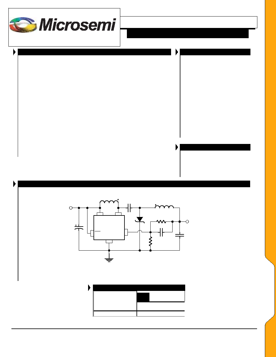
P R O D U C T H I G H L I G H T
C1
10
µ
F
V
IN
= 5V
LX1734
V
IN
SW
L1A
22
µ
H
GND
NFB
C2
1
µ
F
R2
10k
R1
29.4k
L1B
22
µ
H
C3
22
µ
F
V
OUT
= -5V
@ 150mA
C4
1000pF
Note: L1A and L1B are shown as coupled. Individual inductors can also be used.
C1, C2, C3 are ceramic capacitors
SD
Figure 1
PACKAGE ORDER INFO
LM
Plastic MLPL
6-Pin
T
A
(∞C)
RoHS Compliant / Pb-free
Transition DC: 0452
0 to 85
LX1734CLM
Note: Available in Tape & Reel. Append the letters "TR" to the
part number. (i.e. LX1734CLM-TR)
L
L
X
X
1
1
7
7
3
3
4
4
Microsemi
Microsemi Integrated Products
11861 Western Avenue, Garden Grove, CA. 92841, 714-898-8121, Fax: 714-893-2570
Page 2
Copyright
©
2002
Rev. 3.0a, 2005-03-14
WWW
.
Microse
m
i
.
CO
M
LX1734
1.0MHz Inverting DC/DC Converter
TM
Æ
A B S O L U T E M A X I M U M R A T I N G S
Supply Voltage (V
IN
), Shutdown (
SD
).................................................... 0 to 10V
SW Voltage....................................................................................... -0.4V to 20V
NFB Voltage.................................................................................................... -2V
Current Into NFB Pin................................................................................... ±1mA
Operating Temperature Range ............................................................0∞C to 85∞C
Maximum Junction Temperature ................................................................. 125∞C
Storage Temperature......................................................................-65∞C to 150∞C
Peak Package Solder Reflow Temperature
(40 second maximum exposure) ..................................................... 260∞C (+0, -5)
Note: Exceeding these ratings could cause damage to the device. All voltages are with respect to
Ground. Currents are positive into, negative out of specified terminal
.
T H E R M A L D A T A
LM
Plastic LM 6-Pin
THERMAL RESISTANCE
-
JUNCTION TO
A
MBIENT
,
JC
8
∞
C/W
Junction Temperature Calculation: T
J
= T
A
+ (P
D
x
JC
).
The
JC
numbers are guidelines for the thermal performance of the device/pc-board
system. All of the above assume no ambient airflow.
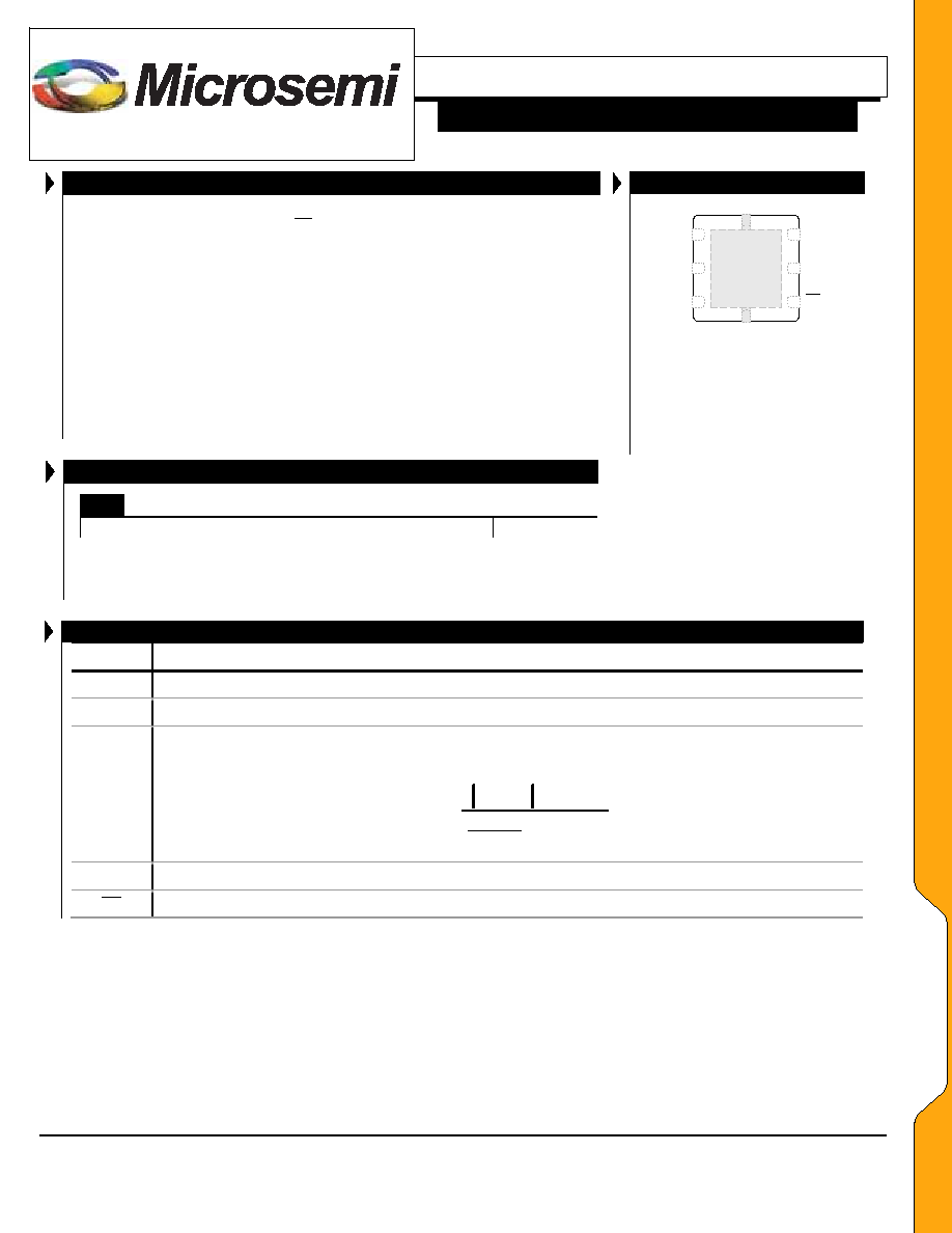
PACKAGE PIN OUT
SW
GND
NFB
SD
V
IN
N/C*
**
LM
P
ACKAGE
(Top View)
* Not Internally Connected.
** Package heatsink should
be connected to ground or
left floating.
RoHS / Pb-free 100% Matte Tin Lead Finish
F U N C T I O N A L P I N D E S C R I P T I O N
N
AME
D
ESCRIPTION
SW
Power Switch Pin
GND
Common ground reference
NFB
Feedback Pin - Connect to a resistive divider in order to set the output voltage. Feedback threshold is -1.235V.
Given the typical NFB bias current (I
NFB
) of 4µA flows out of the pin, the suggested value for R2 is 10K. Given
R
2
, set R
1
according to:
(
)
NFB
I
R
VOUT
R
+
-
=
2
235
.
1
235
.
1
1
V
IN
Input Supply ≠ Input pin must be locally bypassed.
SD
Shutdown, Connected to >2V, device is active.
P
P
A
A
C
C
K
K
A
A
G
G
E
E
D
D
A
A
T
T
A
A
Microsemi
Microsemi Integrated Products
11861 Western Avenue, Garden Grove, CA. 92841, 714-898-8121, Fax: 714-893-2570
Page 3
Copyright
©
2002
Rev. 3.0a, 2005-03-14
WWW
.
Microse
m
i
.
CO
M
LX1734
1.0MHz Inverting DC/DC Converter
TM
Æ
E L E C T R I C A L C H A R A C T E R I S T I C S
Unless otherwise specified, the following specifications apply over the operating ambient temperature 0∞C
T
A
85∞C and the following
test conditions: V
IN
= 5V
LX1734
Parameter Symbol
Test
Conditions
Min Typ Max
Units
Minimum Operating Voltage
V
IN
4.25
V
V
IN
Under Voltage Lockout
UVLO V
IN
rising, regulator remains off
3.2
4.25
V
Reference Voltage
V
NFB
-1.205
-1.235
-1.255
V
Reference Voltage Line Regulation
4.5V
<
V
IN
<
5.5V, T
AMB
> 25∞C
18
mV
NFB Pin Bias Current
I
NFB
-4
-8
µ
A
Quiescent Current
I
Q
(Regulator Not Switching, V
NFB
= -2V)
9
12
mA
Quiescent Current
I
SHDN
SD
V < 0.28V
300
µA
Switching Frequency
I
OUT
= 5mA to 250mA
0.8
1.4
MHz
Maximum Duty Cycle
82 %
Switch V
CESAT
I
SW
= 600mA
650
800
mV
Switch Leakage Current
V
SW
= 10V
0.02
1
µ
A
Switch Circuit Current Limit
Duty Cycle < 50%
700
mA
High
V
SDH
Device
Active
2
V
Low
V
SDL
Device
Disabled
0.8 V
SD
V = 0.28V
-5 0.4 1.0 µA
Shutdown Input Voltage
Bias
Current
I
SD
SD
V = 5V
30
50
µA
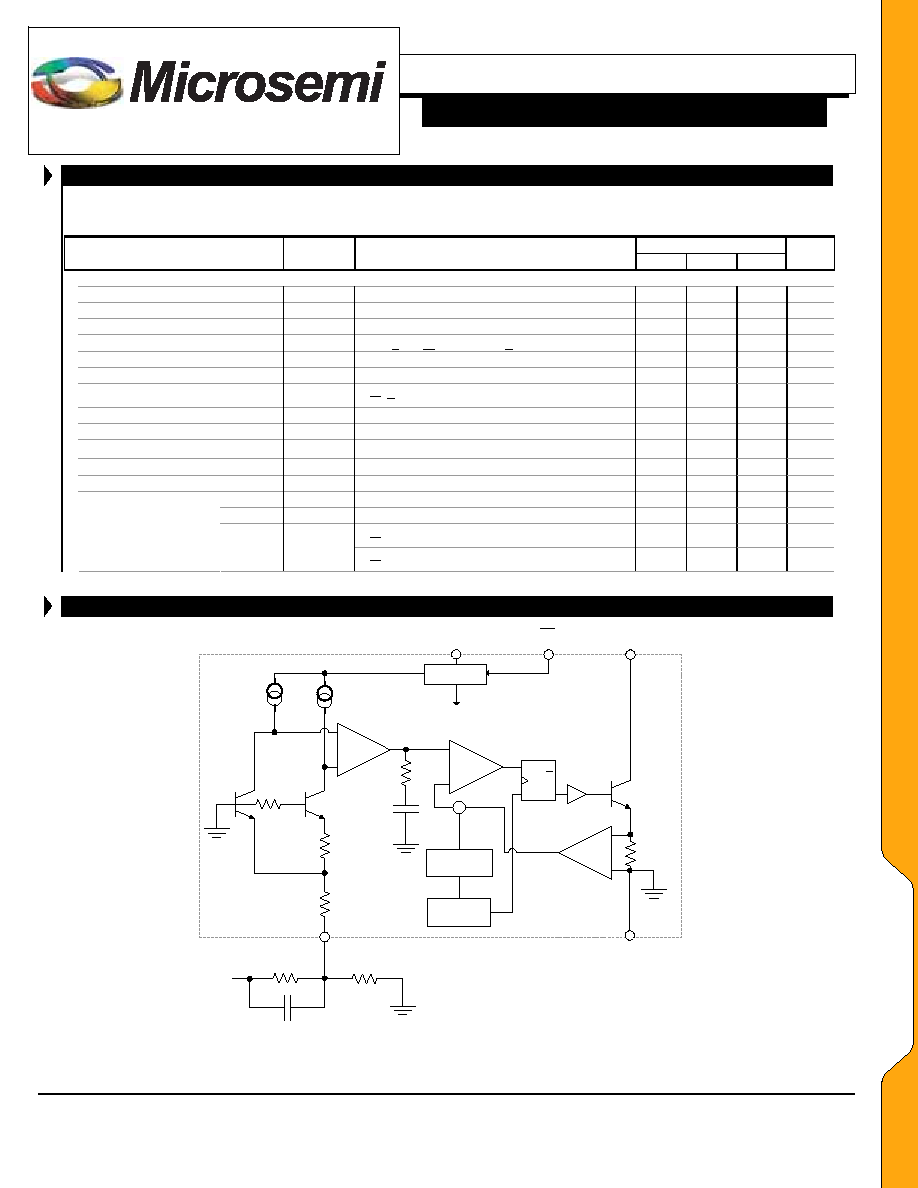
B L O C K D I A G R A M
Q2
Q1
V
IN
NFB
100k
40pF
Q
Q
SET
CLR
S
R
Q3
0.1
SW
GND
Ramp
Generator
1.1MHz
Oscillator
+
-
+
-
-
+
R1 (External)
R2 (External)
C
PL
V
OUT
UVLO
SD
BIAS
Figure 2 ≠ Simplified Block Diagram
E
E
L
L
E
E
C
C
T
T
R
R
I
I
C
C
A
A
L
L
S
S

Microsemi
Microsemi Integrated Products
11861 Western Avenue, Garden Grove, CA. 92841, 714-898-8121, Fax: 714-893-2570
Page 4
Copyright
©
2002
Rev. 3.0a, 2005-03-14
WWW
.
Microse
m
i
.
CO
M
LX1734
1.0MHz Inverting DC/DC Converter
TM
Æ
CONDITIONS: V
IN
@ 5V, V
OUT
@ -5V, C
IN
=
COUT
=10uF Ceramic, L1=L2=10uH
STEP LOAD RESPONSE 0 ≠ 100mA
STEP LOAD RESPONSE 0 ≠ 250mA
POWER ON RESPONSE, IOUT @ 200mA
OUTPUT VOLTAGE RIPPLE, IOUT @ 10mA and 150 mA
LX1734 TEMPERATURE STABILITY
IL = 132mA
-5.2
-5.16
-5.12
-5.08
-5.04
-5
-4.96
-4.92
-4.88
-4.84
-15
0
15
30
45
60
75
90
105
120
800
830
860
890
920
950
980
1010
1040
1070
Vout, Volts
FREQ, Khz
TEMP, ∞C
W
W
A
A
V
V
E
E
F
F
O
O
R
R
M
M
S
S
VOUT
VIN
Inductor, 2A/div
VOUT
ISTEP LOAD
VOUT
ISTEP LOAD
IOUT = 10Ma
IOUT = 150mA

Microsemi
Microsemi Integrated Products
11861 Western Avenue, Garden Grove, CA. 92841, 714-898-8121, Fax: 714-893-2570
Page 5
Copyright
©
2002
Rev. 3.0a, 2005-03-14
WWW
.
Microse
m
i
.
CO
M
LX1734
1.0MHz Inverting DC/DC Converter
TM
Æ
T H E O R Y O F O P E R A T I O N
The LX1734 is a fixed frequency current mode controller
designed to develop a negative output voltage from a positive
input voltage. The switching transistor and current sense resistor
are integrated into the part. The PWM functions in a peak current
regulation mode using the amplified error signal to determine the
peak switch current each cycle. Slope compensation is added to
provide stable operation at high duty cycles. A current limit
detector overrides the regulation loop and prevents the switch
current from exceeding the over current threshold level.
The bandgap control circuit keeps Q1 biased on and produces a
reference current (I
REF
) that produces a voltage drop across the
internal resistance that has a positive temperature coefficient.
When this resistor voltage drop is added to the negative temperature
coefficient of the base-emitter voltage drop of Q1, the result is a
temperature compensated reference voltage (V
REF
) at the NFB pin.
The summing node from the external feedback network is
connected directly to NFB pin, which is relatively high impedance
(typically 150k). The feedback loop minimizes the error current,
(I
ERROR
) which effectively regulates the voltage at the NFB pin. As
with a conventional error amplifier, the error signal is proportional
to the difference between the temperature compensated reference
voltage (V
REF
) and the summing node voltage. A slight correction
factor is necessary to account for the added summing node voltage
due to the reference current (I
REF
, typically 4µADC) flowing
through the Thevenin equivalent summing node external resistance.
A P P L I C A T I O N N O T E
The LX1734 can be used in several topologies that generate a
negative output voltage from a positive input voltage. The
LX1734 can be used in a dual inductor converter with coupled or
uncoupled inductors (see Figure 1); this topology is required if
the absolute value of the output voltage is less than or equal to
the input voltage but can also be used for higher voltage outputs.
The following components or their equivalents can be used to
implement the converter in Figure 1, which produces a ≠5V
output at 150mA from a +5V input. The reference design has an
efficiency of greater than 72% and an input ripple voltage of less
than 6mV
P-P
and an output ripple voltage of less than 300µV
P-P
.
Ref Description
Part
Number Manufacturer
C1 Ceramic,
4.7uF,
6.3V (0805)
JMK212BJ475MG Taiyo
Yuden
C2
Ceramic, 1uF, 16V
(0805)
GRM40X7R105M16 Murata
C3 Ceramic,
22uF,
6.3V (1210)
JMK325BJ226MM Taiyo
Yuden
C4 Ceramic,
470pF,
50V (0402)
GRM36X7R471K050 Murata
D1
Diode, 0.5A, 30V
UPS530
Microsemi
L1 Inductor,
Coupled,
22uH
CLS62-220NC Sumida
Table 1 - Part List for Figure 1 (All Parts Are Surface Mount).
Separate inductors (not on a common core) can be used in place
of the coupled inductor (L1) of Figure 1. In this case the only
component that changes in the parts list is L1, which now would
be two separate inductors (L1, formerly L1A, and L2, formerly
L1B). With the separate inductors the peak-to-peak voltage
ripple on the input the output were less the 2mV
P-P
and less than
500µV
P-P
, respectively.
Table 2 - Part List For Alternative Inductors
Ref.
Designator
Description Part
Number
Manufacturer
L1, L2
Inductor, 47uH,
(1812)
LQH4C470K04M00 Murata
Inductor Selection
When the LX1734 is used in a dual inductor converter with coupled
inductors, a parallel winding inductor value of 22µH works well for
a 5V input and a -5V output at 150mA. The inductor value can be
scaled to the particular set of operating conditions based on the
input voltage, output voltage, and output current. The new value of
coupled inductor parallel inductance can be calculated using the
following equation:
-
◊
◊
◊
=
OUT
OUT
IN
NEW
V
V
5
I
mA
150
V
5
V
µH
22
L
The inductor value should be rounded to the nearest available value.
The parallel saturation current rating of a coupled inductor should
be sized to carry the summation of the peak input and peak output
inductor currents.
When the LX1734 is used in a dual inductor converter with two
separate (uncoupled) inductors or when using the boost converter
with an inverting charge pump output configuration, the inductance
value for each inductor should be about twice the value
recommended for a coupled inductor.
The peak current in the inductor is the DC current plus Ω of the
peak-to-peak ripple current. The saturation current rating of the
inductors should be sized to carry the peak inductor current. The
peak-to-peak ripple current can be calculated based on the inductor
value, the terminal voltage (input or output), and the duty cycle.
The DC inductor current is the same as the DC output current on the
output inductor. The DC input current includes the power for the
LX1734, but is still a good approximation for the DC inductor
current for higher power applications. For simplicity, the
calculations below ignore the voltage drops of the switch and diode.
The duty cycle, D, for the dual inductor topology (assuming
continuous inductor current mode operation) is approximately:
A
A
P
P
P
P
L
L
I
I
C
C
A
A
T
T
I
I
O
O
N
N
Microsemi
Microsemi Integrated Products
11861 Western Avenue, Garden Grove, CA. 92841, 714-898-8121, Fax: 714-893-2570
Page 6
Copyright
©
2002
Rev. 3.0a, 2005-03-14
WWW
.
Microse
m
i
.
CO
M
LX1734
1.0MHz Inverting DC/DC Converter
TM
Æ
A P P L I C A T I O N N O T E ( C O N T I N U E D )
(
)
0
V
where
OUT
<
-
=
IN
OUT
OUT
V
V
V
D
For example, the duty cycle for +5V = VIN and ≠3.3V = VOUT
is 40%.
The duty cycle for the Inverting Charge Pump Output topology
(assuming continuous inductor current mode operation) is
approximately:
0
V
where
OUT
<
+
=
OUT
IN
V
V
1
D
For example, the duty cycle for +5V = VIN and ≠12V = VOUT is
58%.
The peak-to-peak ripple current in the input inductor is
approximately:
(
)
(
)
frequency)
switching
(the
1.0MHz
Fsw
where
Fsw
L
D
V
I
IN
IN
RIPPLEpp
=
◊
◊
=
For example, with a +5V input and a-12V output in an Inverting
Charge Pump Output topology with a 47µH inductor, the peak-to-
peak input ripple is 52mA.
In the dual inductor topology with separate inductors, the peak-
to-peak ripple current in the output inductor is approximately:
(
)
[
]
(
)
Fsw
L
D
1
V
I
OUT
OUT
pp
RIPPLE
◊
-
◊
-
=
For example, with a +5V input and a -3.3V output in a dual
inductor topology with a 47µH output inductor, the peak-to-peak
output ripple is 35mA.
There are many inductor models from many different
manufacturers that work well with the LX1734. Some sources
are listed in Table 5. Ferrite core inductors are recommended to
reduce core losses due to the high operating frequency of the
LX7134. Using inductors with low DC resistance will further
reduce efficiency losses.
Vendor Phone
URL
Part Comments
CLS62-22022
22µH
Coupled
Sumida
(847)
956-0666
www.sumida.com
CD43-470 47µH
Murata
(404)
436-1300
www.murata.com LQH3C-220
22µH, 2mm
Height
Coiltronics
(407)
241-7876
www.coiltronics.com CTX20-1
20µH,
Coupled,
Low DCR
Table 5 ≠ List of Inductor Vendors
Capacitor Selection
To minimize ripple voltage, only capacitors with low series
resistance (ESR) are recommended. Mutli-layer ceramic capacitors
with X5R or X7R dielectric are an excellent choice featuring small
size, very low ESR, and a temperature stable dielectric. The level
shifting capacitor, C2 (of Figure 1), should have a value of 1µF and
a voltage difference between the input and output voltages. The
input and output capacitors (C1 and C2, respectively) should have
values in the range of 1µF or larger. If the inductor ripple current is
known, the ripple voltage can be estimated by the following
equation:
(
)
(
)
V
C
2
L
I
V
PPRIPPLE
2
PP(RIPPLE)
◊
◊
◊
=
Since ripple voltage is inversely proportional to the capacitor value,
larger value ceramic capacitors will result in lower ripple voltages.
When using a ceramic capacitor for the output capacitor, it is
recommended that a phase lead network be inserted in the feedback
loop to improve the transient response. This can be accomplished
by placing a capacitor in parallel with resistor R1 (see Figure 1).
The corner frequency for the phase lead zero is between 20KHz and
60KHz. C4 can be calculated using the following equation:
(
)
4
C
1
R
2
1
◊
◊
=
z
f
Electrolytic capacitors such as solid tantalum or OS-CON types can
also be used with consideration for the ESR. Since ESR adds to the
capacitor reactive impedance, ESR will increase the ripple voltage.
The electrolytic output capacitor impedance has a built in zero, so
adding C4 is usually not required when using an electrolytic
capacitor.
Diode Selection
A Schottky diode is recommended for use with the LX1734. The
Microsemi UPS530 (30V @ 0.5A) or Microsemi UPS5817 (20V @
1A) are good choices.
Layout Considerations
In operation, current is transferred between the LX1734 and D1 so
to minimize ground noise it is recommended that the D1 cathode be
connected directly to the ground pin pad for the LX1734 (refer to
figure 1). When laying out the converter, to minimize EMI, it is
important to minimize the area enclosed within the main current
loops. It is also important to minimize the length of etch connecting
to pin 3 (NFB) and to minimize the total trace area on both sides of
C2. A ceramic bypass capacitor should be connected between pin 5
(VIN) and pin 2 (GND) and located in close proximity to the
LX1734.
A
A
P
P
P
P
L
L
I
I
C
C
A
A
T
T
I
I
O
O
N
N
Microsemi
Microsemi Integrated Products
11861 Western Avenue, Garden Grove, CA. 92841, 714-898-8121, Fax: 714-893-2570
Page 7
Copyright
©
2002
Rev. 3.0a, 2005-03-14
WWW
.
Microse
m
i
.
CO
M
LX1734
1.0MHz Inverting DC/DC Converter
TM
Æ
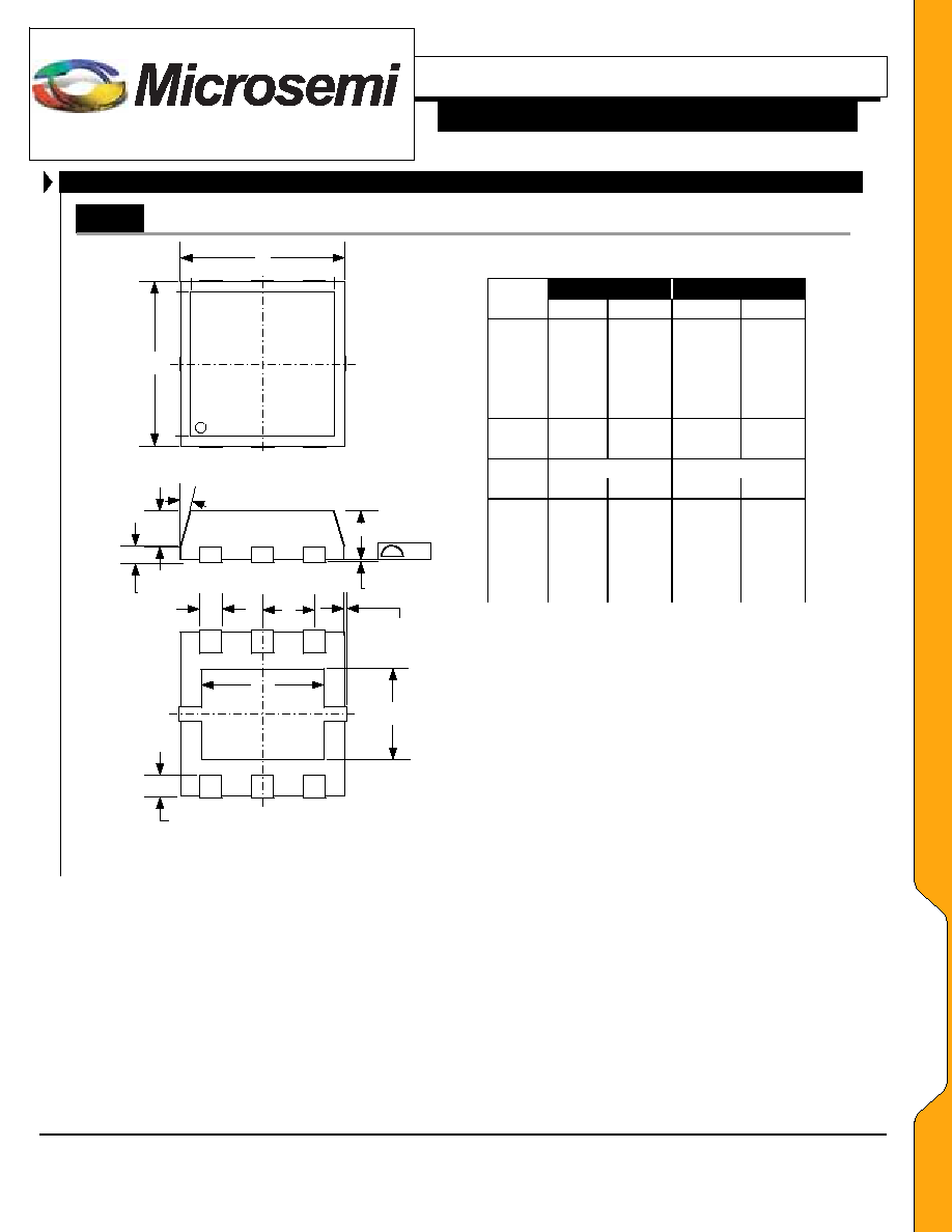
P A C K A G E D I M E N S I O N S
LM
6-Pin Plastic Exposed Pad JEDEC MO-229 Reference
e
D2
E2
A
A2
TOP VIEW
SIDE VIEW
BOTTOM VIEW
L
b
E
D
.08
A1
A3
L2
M
ILLIMETERS
I
NCHES
Dim
MIN MAX MIN MAX
A 0.80 1.05 0.031 0.041
A1 * 0.05 0.002
A2 0.65 0.75 0.025 0.295
A3 0.15 0.25 0.006 0.010
b 0.33 0.45 0.012 0.017
D 2.90 3.10 0.114 0.122
E 2.90 3.10 0.114 0.122
e
0.95 BSC
0.037 BSC
D2 1.78 2.34 0.070 0.092
E2 1.01 1.57 0.039 0.061
L 0.20 0.45 0.007 0.017
L2 --- 0.13 --- 0.005
K 0.20 * 0.007 *
0∞ 12∞ 0∞ 12∞
Note:
1. Dimensions do not include mold flash or protrusions;
these shall not exceed 0.155mm(.006") on any side.
Lead dimension shall not include solder coverage.
M
M
E
E
C
C
H
H
A
A
N
N
I
I
C
C
A
A
L
L

Microsemi
Microsemi Integrated Products
11861 Western Avenue, Garden Grove, CA. 92841, 714-898-8121, Fax: 714-893-2570
Page 8
Copyright
©
2002
Rev. 3.0a, 2005-03-14
WWW
.
Microse
m
i
.
CO
M
LX1734
1.0MHz Inverting DC/DC Converter
TM
Æ
N O T E S
PRODUCTION DATA ≠ Information contained in this document is proprietary to
Microsemi and is current as of publication date. This document may not be modified in
any way without the express written consent of Microsemi. Product processing does not
necessarily include testing of all parameters. Microsemi reserves the right to change the
configuration and performance of the product and to discontinue product at any time.
N
N
O
O
T
T
E
E
S
S