Replacement of
TL064C
MIK064C
Quad Low Power J-FET
Operational Amplifier
November 2001 - revised June 2002
Features
∑
Very low power consumption: 200µA
∑
Wide common-mode (up to V
CC
+
) and differential voltage ranges
∑
Low input bias and offset currents
∑
Output short-circuit protection
∑
High input impedance J-FET input stage
∑
Internal frequency compensation
∑
Latch up free operation
∑
Latch up free operation
∑
High slew rate: 3.5V/µs
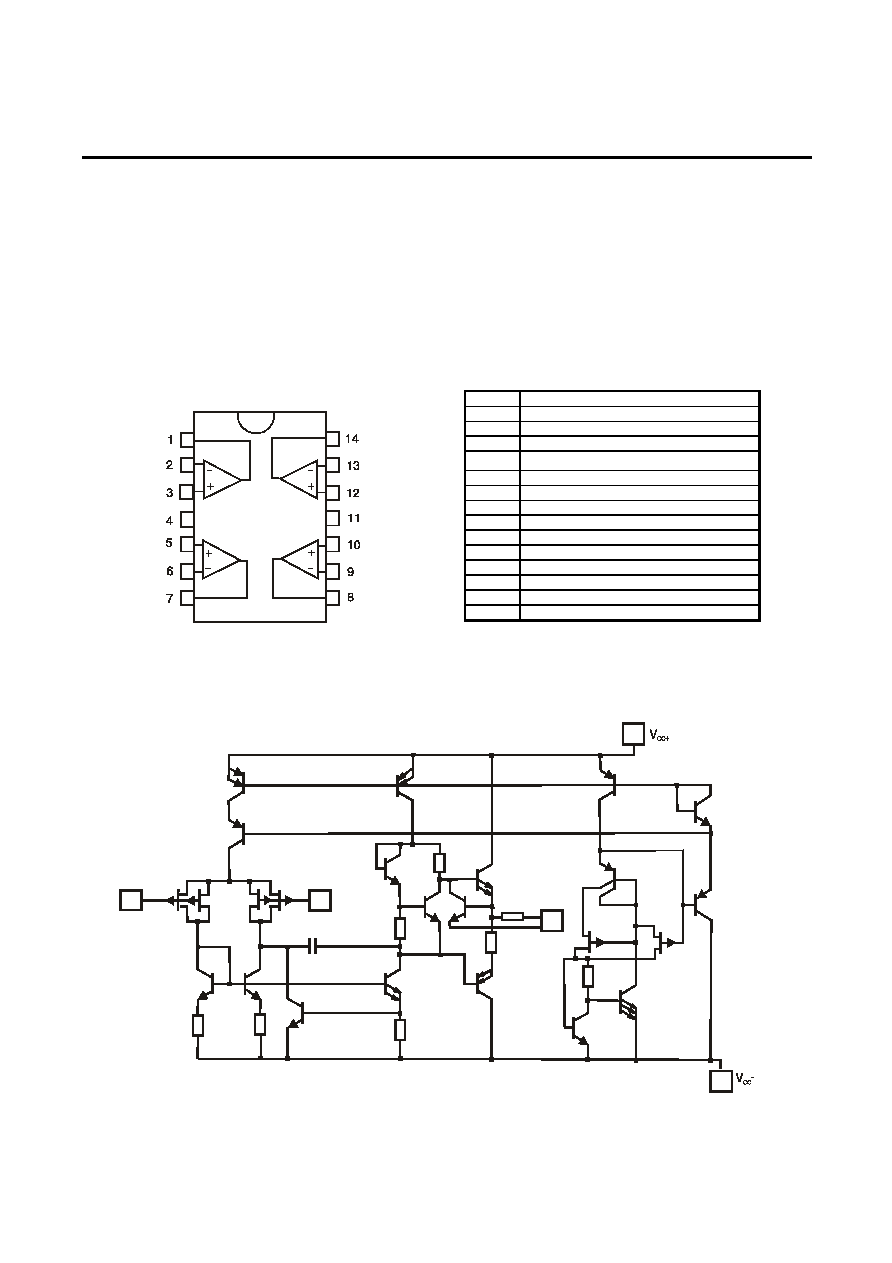
Pin Connections
(top view)
Pad N
Pad Name
1 Output
1
2
Inverting input 1
3
Non-inverting input 1
4 V
CC
+
5
Non-inverting input 2
6
Inverting input 2
7 Output
2
8 Output
3
9
Inverting input 3
10
Non-inverting input 3
11 V
CC
-
12
Non-inverting input 4
13
Inverting input 4
14 Output
4
Schematic Diagram
Non inverting
input
Inverting
input
42 k
100
270
45 k
64
220
32 k
1/4 MIK064C
Page 1 of 3
Replacement of
TL064C
MIK064C
Quad Low Power J-FET
Operational Amplifier
November 2001 - revised June 2002
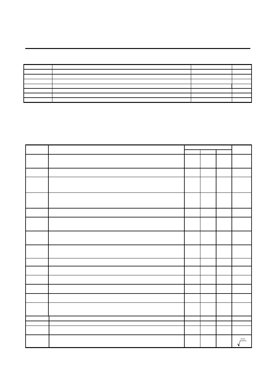
Absolute Maximum Ratings
Symbol Parameter
Value
Unit
V
CC
Supply Voltage ≠ (Note 1)
±18
V
V
i
Input Voltage ≠ (Note 3)
±15
V
V
id
Differential Input Voltage ≠ (Note 2)
±30
V
P
tot
Power Dissipation
680 mW
Output Short-circuit Duration (Note 4)
Infinite
T
oper
Operating Free-Air Temperature Range MIK062C
0 to 70
0
C
T
stg
Storage Temperature Range
-65 to +150
0
C
Note 1: All voltage values, except differential voltage, are with respect to the zero reference level (ground) of the supply voltages where
the zero reference level is the midpoint between V
CC
+
and V
CC
-
.
Note 2: Differential voltages are at the non-inverting input terminal with respect to the inverting input terminal.
Note 3: The magnitude of the input voltage must never exceed the magnitude of the supply voltage or 15 volts, whichever is less.
Note 4: The output may be shorted to ground or to either supply. Temperature and/or supply voltages must be limited to ensure that the
dissipation rating is not exceeded.
Electrical Characteristics
V
CC
=
± 15V, T
AMB
= 25
∞C (unless otherwise specified)
TL064C
Symbol
Parameters
Min Typ Max
Units
V
IO
Input Offset Voltage (R
S
= 50
)
T
amb
=25
∞C
T
min.
T
amb.
T
max.
3
15
20
mV
DV
IO
Temperature Coefficient of Input Offset Voltage (R
S
= 50
)
10
µV/∞C
I
IO
Input Offset Current
*
T
amb
=25
∞C
T
min.
T
amb.
T
max.
5
200
5
pA
nA
I
IB
Input Bias Current
*
T
amb
=25
∞C
T
min.
T
amb.
T
max.
30
400
10
pA
nA
V
ICM
Input Common Mode Voltage Range
±11
+15
-12
V
V
OPP
Output Voltage Swing (R
L
= 10k
)
T
amb
=25
∞C
T
min.
T
amb.
T
max.
20
20
27
V
A
VD
Large Signal Voltage Gain (R
L
= 10k
, V
O
=
± 10V)
T
amb
=25
∞C
T
min.
T
amb.
T
max.
3
3
6
V/mV
GBP
Gain Bandwidth Product
(T
amb
=25
∞C, R
L
= 10k
,
C
L
=100pF)
1
MHz
R
I
Input Resistance
10
12
CMR
Common Mode Rejection Ratio
(R
S
= 50
)
70
76
dB
SVR
Supply Voltage Rejection Ratio
(R
S
= 50
)
70
95
dB
I
CC
Supply Current (Per Amplifier)
(T
amb
=25
∞C, no load, no signal)
200
250
µA
V
O1
/V
O2
Channel Separation
(A
V
=100, T
amb
=25
∞C)
120
dB
P
D
Total Power Consumption
(Each Amplifier)
(T
amb
=25
∞C, no load, no signal)
6
7.5
mW
SR
Slew Rate (V
i
= 10V, R
L
= 10k
, C
L
= 100pF, A
V
= 1)
1.5 3.5 V/
µs
t
r
Rise Time (V
i
= 20mV, R
L
= 10k
, C
L
=100pF, A
V
= 1)
0.2
µs
K
OV
Overshoot Factor (V
i
= 20mV, R
L
= 10k
, C
L
=100pF, A
V
= 1)
(see figure 1)
10 %
e
n
Equivalent input Noise Voltage
(R
S
= 100
, f = 1KHz)
42
nV
Hz
* - Input bias currents of a FET- input operational amplifier are normal junction reverse currents, which are temperature sensitive.
Pulse techniques must be used that will maintain the junction temperature as closes to the ambient temperature as possible.
Page 2 of 3