Replacement of
LT1083/84/85
MIK1083/84/85
Low Dropout Positive
Adjustable Voltage Regulators
May 1995 - revised September 2002
Description
The MIK1083/MIK1084/MIK1085 series of positive adjustable regulators are designed to provide 7.5A, 5A and 3A with higher efficiency
than currently available devices. All internal circuitry is designed to operate down to 1V input to output differential and the dropout
voltage is fully specified as a function of load current. Dropout is guaranteed at a maximum of 1.5 V at maximum output current. On-chip
trimming adjusts the reference voltage to 1%. Current limit is also trimmed, minimizing the stress on both the regulator and power
source circuitry under overload conditions.
The MIK1083/MIK1084/MIK1085 devices are pin compatible with older 3 terminal regulators. A 10µF output capacitor is required on
these new devices; however, this is usually included in most regulator designs.
Features
∑ Three Terminal Adjustable
∑ Output Current of 3A, 5A or 7.5A
∑ Operates Down to 1V dropout
∑ Guaranteed Dropout Voltage at Multiple Current Levels
∑ 0.015% Line Regulation
∑ 0.01% Load Regulation
∑ 100% Thermal Limit Burn-In
Applications
∑
High Efficiency Linear Regulators
∑
Post Regulators for Switching Supplies
∑
Constant Current Regulators
∑
Battery Chargers
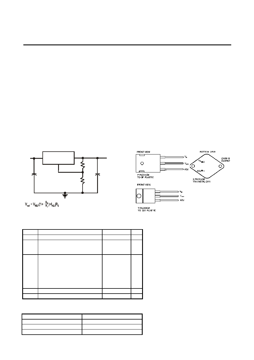
Typical application data 5V, 5A
regulator
MIK1084
V = 5V
I = 5A
0
0
C1 = 10 F
µ
1 F*
TANTALUM
µ
121
1%
365
1%
1
2
+
* REQUIRED FOR STABILITY
R1
R2
+
3
V
IN
6.5W
Package information
Absolute Maximum Ratings
Symbol Parameter
Maximum
Units
P
D
Power Dissipation
Internally Limited
W
V
IN
Input to Output Voltage Differential
´Mª Grades
´Cª Grades
35
30
V
T
J
Operating Junction Temperature Range
´Mª Grades
Control Section
Power Transistor
´Cª Grades
Control Section
Power Transistor
-55 to 150
-55 to 200
0 to 125
0 to150
o
C
T
STG
Storage Temperature
-65 to 150
o
C
T
LEAD
Lead Temperature (Soldering, 10 sec)
300
o
C
Device Selection Guide
Device Output
Current
MIK1083 7.5A
MIK1084 5.0A
MIK1085 3.0A
Page 1 of 3

Replacement of
LT1083/84/85
MIK1083/84/85
Low Dropout Positive
Adjustable Voltage Regulators
May 1995 - revised September 2002
Electrical Characteristics
(Note 1)
Parameter
Test Conditions
Min
Typ
Max
Units
Reference Voltage
I
OUT
= 10mA, T
j
=25
∫
C
(V
IN
- V
OUT
) = 3V (K Package Only)
1.238 1.250 1.262 V
10mA
I
OUT
I
FULL LOAD
1.5V
(V
IN
- V
OUT
)
25V (Note 3)
*
1.225
1.250
1.270
Line Regulation
I
LOAD
=10mA, 1.5
(V
IN
- V
OUT
)
15V,
T
j
= 25
∫
C
M Grade
15V
(V
IN
- V
OUT
)
35V
C Grade
15V
(V
IN
- V
OUT
)
30V (Notes 1,2)
*
*
*
0.015
0.035
0.05
0.05
0.2
0.2
0.5
0.5
%
Load Regulation
(V
IN
- V
OUT
) = 3V
10mA
I
OUT
I
FULL LOAD
T
j
= 25
∫
C (Notes 1,2,3,5)
*
0.1
0.2
0.3
0.4
%
Dropout Voltage
V
REF
=
1%, I
OUT
= I
FULL LOAD
(Notes 4,5)
* 1.3 1.5 V
Current Limit
MIK1083
MIK1084
MIK1085
(V
IN
- V
OUT
) = 5V
(V
IN
- V
OUT
) = 25V
(V
IN
- V
OUT
) = 5V
(V
IN
- V
OUT
) = 25V
(V
IN
- V
OUT
) = 5V
(V
IN
- V
OUT
) = 25V
*
*
*
*
*
*
8.0
0.4
5.5
0.3
3.2
0.2
9.5
1.0
6.5
0.6
4.0
0.5
A
Minimum Load Current
(V
IN
- V
OUT
) = 25V
*
5
10
mA
Termal Regulation
MIK1083
MIK1083
MIK1085
T
A
= 25
∫
C, 30ms pulse
0.002
0.003
0.004
0.01
0.015
0.02
%/W
Ripple Rejection
f = 120Hz,
C
ADJ
=25µF, C
OUT
=25µF Tantalum,
I
OUT
= I
FULL LOAD
, (V
IN
- V
OUT
) = 3V (Note 5)
*
60
75
dB
Adjust Pin Current
T
j
= 25
∫
C
*
55
120
Adjust Pin Current Change
10mA
I
OUT
I
FULL LOAD
,
1.5V
(V
IN
- V
OUT
) = 25V (Note 5)
*
0.2
5
µA
Temperature
Stability
* 0.5
Long Term Stability
T
A
= 125
∫
C, 1000Hrs
0.3
1
RMS Output Noise (% of V
OUT
) T
A
= 25
∫
C,
10Hz
f 10kHz
0.003
%
The * denotes the specifications which apply over the full operating temperature range.
Note 1: See thermal regulation specifications for changes in output voltage due to heating effects. Load and line regulation are
measured at a constant junction temperature by low duty cycle pulse testing.
Note 2: Line and load regulation are guaranteed up to the maximum power dissipation (60W for the MIK1083, 45W for the
MIK1084(K,P), 30W for the MIK1084(T) and 30W for the MIK1085). Power dissipation is determined by the input/output
differential and the output current. Guaranteed maximum power dissipation will not be available over the full input/output
voltage range.
Note 3: I
FILL LOAD
is defined in the current limit curves. I
FILL LOAD
curve is defined as the minimum value of current limit as a function of input
to output voltage.
Note 4: Dropout voltage is specified over the full output current range of the device.
Note 5: For MIK1083 I
FILL LOAD
is 5A for -55
∫
C
Tj -40
∫
C and 7.5A for Tj > -40
∫
C
Page 2 of 3

Replacement of
LT1083/84/85
MIK1083/84/85
Low Dropout Positive
Adjustable Voltage Regulators
May 1995 - revised September 2002
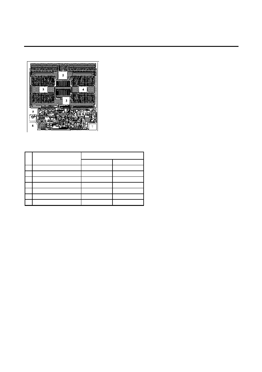
Pad Location MIK1083/ MIK1084/ MIK1085
Chip size 3.1mm x 3.05mm
Pad Location Coordinates
Coordinates (µm)
N Pad
Name
X Y
1 INPUT
1370
2280
2 INPUT
1530
1190
3 OUTPUT
520
1720
4 OUTPUT
2245
1720
5 OUTPUT
100
760
6 ADJUST
100
100
7 NC
2660
100
Page 3 of 3


