Replacement of
LP2950-XX/LP2951-XX
MIK2950-XX/MIK2951-XX
100 mA Low Dropout
Positive Voltage Regulator
October 1995 - revised September 2002
Description
The MIK2950-XX/MIK2951-XX is a low power voltage regulator. This device excellent choice for use in battery powered application such
as cordless telephone, radio control systems, and portable computers.
The MIK2950-XX/MIK2951-XX features very low quiescent current (75µA Typ.) and very low drop output voltage (Typ. 40mV at light
load and 380mV at 100mA). This includes a tight initial tolerance of 0.5% typ., extremely good load and line regulation of 0.05% typ.,
and very low output temperature coefficient, making the MIK2950-XX/MIK2951-XX useful as a low-power voltage reference.
The error flag output feature is used as power-on reset for warn of a low output voltage, due to following batteries on input. Other feature
is the logic-compatible shutdown input which enable the regulator to be switched on and off. The MIK2951-XX is available in 8-pin
plastic packages. The regulator output voltage may be pin-strapped for a -XX volt or programmed from 1.24 volt to 29 volts with external
pair of resistors.
The MIK2950-XX is offered in 3-pin TO-92 package compatible with other fixed regulator.
Features
∑
High accuracy output voltage
∑
Guaranteed 100mA output
∑
Very low quiescent current
∑
Low dropout voltage
∑
Extremely tight load and line regulation
∑
Very low temperature coefficient
∑
Needs only 1mF for stability
∑
Error Flag warns of output dropout
∑
Logic-Controlled electronic shutdown
∑
Output programmable from 1.24 to 29V
Applications
∑ Battery
powered systems
∑ Cordless telephones
∑ Radio control systems
∑ Portable/Palm top/Notebook computers
∑ Portable consumer equipment
∑ Portable Instrumentation
∑ Avionics
∑ Automotive Electronics
∑ SMPS Post-Regulator
∑ Voltage Reference
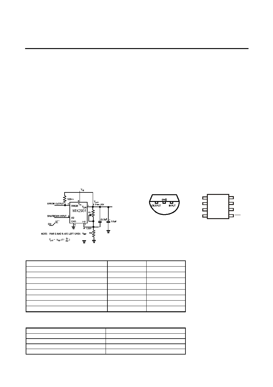
Typical application data 100 mA
adjustable regulator
Package information
Top view
TO-92 Plastic
Package
(MIK2950-XX only)
Pin Connection MIK2951-XX
1
8
3
6
4
5
input
output
feedback
sense
-XX V tap
shutdown
error
ground
2
7
MIK2951-XX
Absolute Maximum Ratings
Parameter Maximum
Units
Power Dissipation
Internally Limited
W
Lead Temperature (Soldering, 5 seconds)
260
∞C
Storage Temperature Range
-65 to+150
∞C
Operating Junction Temperature Range
-55 to +150
∞C
Input Supply Voltage
-0.3 to +30
V
Feedback Input Voltage
-1.5 to +30
V
Shutdown Input Voltage
-0.3 to +30
V
Error Comparator Output
-0.3 to +30
V
Device Selection Guide
(Note 1)
Device
Output voltage
MIK2950-2.85, MIK2951-2.85 2.85
MIK2950-3.0, MIK2951-3.0 3.0
MIK2950-3.3, MIK2951-3.3 3.3
MIK2950-5.0, MIK2951-5.0 5.0
Note 1: Other versions are available Vout = 2.9V to 5.0V
Page 1 of 3
Replacement of
LP2950-XX/LP2951-XX
MIK2950-XX/MIK2951-XX
100 mA Low Dropout
Positive Voltage Regulator
October 1995 - revised September 2002
Electrical Characteristics
Electrical Characteristics at Ta = 25oC, VIN = 15V; unless otherwise noted
Parameter Test
Conditions
(Note 2) Min
Typ
Max
Units
Output Voltage
-25
∞CT
J
85∞C
Full Operating Temperature
0.985 |V
0
|
0.98 |V
0
|
V
0
1.015
|V
0
|
1.02 |V
0
|
Output Voltage
100µA
I
L
100mA, T
J
T
JMAX
0.976|V
0
| V
0
1.024
|V
0
|
V
Output Voltage Temperature Coefficient
(Note 1)
50
150
ppm/
∞C
Line Regulation (Note 3)
V
0
+ 1V
V
in
30V (Note 4)
0.04
0.4 %
Load Regulation (Note 3)
100µA
I
L
100mA
0.1
0.3 %
Dropout Voltage (Note 5)
I
L
=100 µA
I
L
=100 mA
50
380
80
450
mV
Ground Current
I
L
=100 µA
I
L
=100 mA
75
8
120
12
µA
mA
Dropout Ground Current
V
in
=V
0
- 0.5V, I
L
=100 µA
110
170
µA
Current Limit
Vout=0
160
200
mA
Thermal Regulation
0.05
0.2
%/W
Output Noise, 10Hz to 100KHz
C
L
=1µF
C
L
=200µF
C
L
=3.3µF
(Bypass=0.01 µF pins 7 to 1
(MIK2951-XX))
430
160
100
µV
rms
8-pin Versions only
Reference
Voltage
1.21 1.235 1.26
Reference Voltage
Over Temperature (Note 6)
1.185
1.285
V
Feedback Pin Bias Current
20
40
nA
Reference Voltage Temperature Coefficient
(Note 7)
50
ppm/
∞C
Feedback Pin Bias Current Temperature Coefficient
0.1
nA/
∞C
Error Comparator
Output Leakage Current
Voh=30V
0.01
1.0
µA
Output Low Voltage
Vin=4.5V, I
OL
=400 µA
150
250
Upper Threshold Voltage
(Note 8)
40
60
Lower Threshold Voltage
(Note 8)
75
95
Hysteresis (Note
8)
15
mV
Shutdown Input
Input Logic Voltage
Low (Regulator ON)
High (Regulator OFF)
2
1.3 0.7 V
Shut down Pin Input Current
V
S
=2.4V
V
S
=30V
30
450
50
600
(Note 9)
V
OUT
= 5.0 V
3
10
3.3V
V
OUT
< 5.0 V
20
Regulator Output Current in Shutdown
2.0V
V
OUT
< 3.3 V
30
µA
Note 1: Output or reference voltage temperature coefficients defined as the worst case voltage change divided by the total temperature
range.
Note 2: Unless otherwise specified all limits guaranteed for T
J
= 25
∞C, Vin = V
0
+ 1V, I
L
= 100µA and C
L
= 1µF. Additional conditions for
the 8-pin versions are feedback tied to -XX V tap and output tied to output Sense (V
out
= XX V) and V
shutdown
0.8 V
Note 3: Regulations is measured at constant junction temperature, using pulse testing with a low duty cycle. Changes in output voltage
due to heating effects are covered under the specification for thermal regulation.
Note 4: Line regulation for MIK2951-XX is tested at 150
∞C for I
L
= 1mA. For I
L
= 100µA and T
J
= 125
∞C, line regulation is guaranteed by
design to 0.2%. See typical performance characteristics for line regulation versus temperature and load current.
Note 5: Dropout voltage is defined as the input to output differential at which the output voltage drops 100mV below its nominal value
measured at 1V differential. At very low values of programmed output voltage, the minimum input supply voltage of 2V (2.3V over
temperature) must be taken into account.
Note 6: Vref
Vout (Vin - 1V), 2.3V Vin 30V, 100µA I
L
100mA, T
J
T
JMAX.
Note 7: Output or reference voltage temperature coefficient is defined as the worst case voltage change divided by the total temperature
range.
Note 8: Comparator thresholds are expressed in terms of a voltage differential at the feedback terminal below the nominal reference
voltage measured at V
0
+ 1V input. To express these thresholds in terms of output voltage change, multiply by the error amplifier
Page 2 of 3
Replacement of
LP2950-XX/LP2951-XX
MIK2950-XX/MIK2951-XX
100 mA Low Dropout
Positive Voltage Regulator
October 1995 - revised September 2002
gain = V
out
/V
ref
= (R1 + R2)/R2. For example, at a programmed output voltage of 5V, the error output is guaranteed to go low when
the output drops by 95mV x 5V/1.235V=384mV. Thresholds remain constant as a percent of Vout as Vout is varied, with the
dropout warning occurring at typically 5% below nominal, 7.5% guaranteed.
Note 9: V
shutdown
2V, Vin 30V, Vout = 0, Feedback pin tied to -XX V Tap.
Block Diagram and Typical Applications
MIK2950-XX
MIK2951-XX
Pad Location MIK2951-XX
(For MIK2950-XX fixed versions see Note 1)
Chip Size: 2.05 x 1.15 mm
Pad Location Coordinates
Coordinates (
µm)
N Pad
Name
X Y
1 Output
440
110
2 Sense
810
110
3 Shutdown
1250
110
4 Ground
1865
110
5 Error
1865
950
6
XX V tap
935
950
7 Feedback
735
950
8 Input
440
950
Note 1: For MIK2950-XX:
8 - connected to Input;
1,2 - connected to Output;
4 - connected to GND.
Page 3 of 3