 | –≠–ª–µ–∫—Ç—Ä–æ–Ω–Ω—ã–π –∫–æ–º–ø–æ–Ω–µ–Ω—Ç: MIK 324 | –°–∫–∞—á–∞—Ç—å:  PDF PDF  ZIP ZIP |

1
MIK324
∑
QUAD OPERATIONAL AMPLIFIERS
MI
KRON
JS
C
∑
h
t
t
p
:/
/
w
w
w
.mi
k
ron.ru
∑
M
a
r
c
h
2003
GENERAL DESCRIPTION
The MIK324 consists of four independent, high gain,
internally frequency compensated operational
amplifiers which were designed specifically to operate
from a single power supply over a wide range of
voltages. Operation from split power supplies is also
possible and the low power supply current drain is
independent of the magnitude of the power supply
voltage.
Application areas include transducer amplifiers, DC gain
blocks and all the conventional op amp circuits which
now can be more easily implemented in single power
supply systems.
For example, the MIK324 can be directly operated off of
the standard +5V power supply voltage which is used in
digital systems and will easily provide the required
interface electronics without requiring the additional
±15V power supplies.
FEATURES
∑
Wide range of supply voltages 3V to 30V
∑
Low supply current drain independent of supply
voltage 1.5mA TYP.
∑
Low input biasing current
∑
Low input offset voltage and offset current
∑
Input common-mode voltage range includes ground
∑
Differential input voltage range equal to the power
supply voltage
∑
DC voltage gain 100V/mV TYP.
∑
Internally frequency compensation
REPLACEMENT
of
LM324
MIK324
LOW POWER QUAD OPERATIONAL AMPLIFIERS
CONTENTS
Page
GENERAL DESCRIPTION
1
FEATURES
1
SCHEMATIC DIAGRAM
2
PIN CONNECTIONS
2
ABSOLUTE MAXIMUM RATINGS
2
CONTENTS
Page
ELECTRICAL CHARACTERISTICS
3
PHYSICAL DIMENSIONS
AND
MARKING
DIAGRAMS
4
SOP-14
4
DIP-14
4
ORDERING INFORMATION
4
DATA SHEET
M
ARCH
2003
N
O
. 00005
R
EV
1-03

Design by Vladimir F.Lityaghin / E-mail: lityaghin@mail.ru / Tel: +7(095)532-64-54
QUAD OPERATIONAL AMPLIFIERS
∑
MIK324
MI
KRON
JS
C
∑
h
t
t
p
:/
/
w
w
w
.mi
k
ron.ru
∑
M
a
r
c
h
2003
2
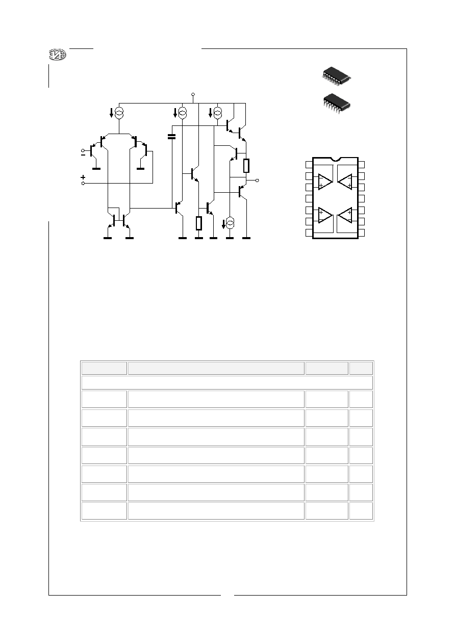
SCHEMATIC DIAGRAM
(º MIK324)
PIN CONNECTIONS
(top view)
DIP-14
SOP-14
MIK324N
MIK324M
14
13
12
11
10
9
8
3_IN +
3_OUT
3_IN --
4_IN +
4_IN --
4_OUT
1_IN --
1_IN +
2_IN --
2_IN +
2_OUT
1_OUT
1
2
3
4
5
6
7
GND
V
CC
1
4
2
3
6 µA
100 µA
4 µA
50 µA
Q12
Q11
Q10
C
C
Q7
Q6
Q5
Q9
Q8
Q4
Q3
Q2
Q1
R
SC
OUTPUT
INVERTING
INPUT
NON-INVERTING
INPUT
V
CC
!
!
!
!
!
!
!
!
!
!
!
!
!
!
!
!
!
ABSOLUTE MAXIMUM RATINGS
SYMBOL
PARAMETER
VALUE
UNIT
POWER
SUPPLY
VOLTAGE
V
CC
Single
supply
32
V
V
CC
,
V
EE
Split
supply
±16
V
V
IDR
Input
differential
voltage
range
±32
V
I
OS
Output
short
-
circuit
to
GND
Continuous
T
J
Junction
temperature
150
∫C
Tstg
Storage
Temperature
-
65
to
+
150
∫C
T
A
Operating
ambient
temperature
range
0
to
+
70
∫C

3
MIK324
∑
QUAD OPERATIONAL AMPLIFIERS
MI
KRON
JS
C
∑
h
t
t
p
:/
/
w
w
w
.mi
k
ron.ru
∑
M
a
r
c
h
2003
ELECTRICAL CHARACTERISTICS
at specified free-air temperature, Vcc = 5 V (unless otherwise noted)
* All characteristics are measured under open-loop conditions with zero common-mode input voltage unless
otherwise specified. "MAX" V
CC
for testing purposes is 30 V. Full range is 0 ∞ to 70 ∞
.
SYMBOL
PARAMETER
TEST CONDITIONS*
MIN
TYP MAX
UNIT
25
∞
3
7
V
IO
Input offset voltage
Vcc = 5 V to MAX,
V
IC
= V
ICR
min,
Vo=1.4 V
Full range
9
mV
V
IO
Average temperature coefficient
of input offset voltage
Full
range
7
µV/
∞
C
25
∞
2
50
l
IO
Input offset current
Vo=1.4 V
Full range
150
nA
l
IO
Average temperature coefficient
of input offset current
Full
range
10
pA/
∞
C
25
∞
-20 -250
I
IB
Input bias current
Vo=1.4 V
Full range
-500
nA
25∞
0 to Vcc-1.5
V
ICR
Common-mode input voltage
range
Vcc = 5 V to MAX
Full range
0 to Vcc≠
2.0
V
R
L
=2
K
25
∞
Vcc-1.5
Vcc = MAX, R
L
=2 k
Full range
26
V
OH
High-level output voltage
Vcc = MAX,
R
L
= 10 k
Full range
27
28
V
V
OL
Low-level output voltage
R
L
= 10 k
Full range
5
20
mV
25
∞
25 100
A
VD
Large-signal differential voltage
amplification
Vcc = 15 V,
Vo=1V to 11 V,
R
L
2 k
Full range
15
V/mV
CMRR
Common-mode rejection ratio
Vcc = 5 V to MAX,
V
IC
= V
ICR
min
25
∞
65
80
dB
k
SVR
Supply voltage rejection ratio
(Vcc/V
IO
)
Vcc = 5 V to MAX
25
∞
65 100
dB
Vo1
/
Vo2
Crosstalk attenuation
f=1 kHz to 20 kHz
25
∞
120
dB
25
∞
-20
-30
Vcc = 15V,
V
ID
=1V, V
O
= 0
Full range
-10
25
∞
10
20
Vcc = 15 V,
V
ID
= - 1 V, Vo = 15V Full range
5
mA
lo
Output current
V
ID
= - 1 V,
Vo =200 mV
25
∞
12
30
µA
l
OS
Short-circuit output current
Vcc at 5 V,
GND at -5 V, Vo=0
25
∞
±40
±60
mA
Vo - 2.5 V, No load
Full range
1.5
2.4
I
CC
Supply current (two amplifiers)
Vcc = MAX,
Vo = 0.5Vcc, No load
Full range
1.1
3
mA

Design by Vladimir F.Lityaghin / E-mail: lityaghin@mail.ru / Tel: +7(095)532-64-54
QUAD OPERATIONAL AMPLIFIERS
∑
MIK324
MI
KRON
JS
C
∑
h
t
t
p
:/
/
w
w
w
.mi
k
ron.ru
∑
M
a
r
c
h
2003
4
ORDERING INFORMATION
ORDERING
NUMBER
PACKAGE
OPERATING
TEMPERATURE
RANGE
SHIPPING
MIK324M
SOP-14
Tube/Rail and Tape/Reel
MIK324N DIP-14
0 to +70∫C
Tube/Rail and Tape/Reel
SOP-14
PACKAGE
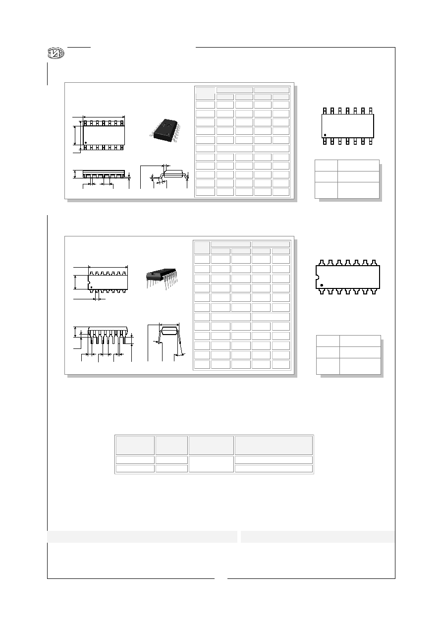
PHYSICAL DIMENSIONS
AND
MARKING DIAGRAMS
DIP-14
PACKAGE
SOP-14
MARKING DIAGRAM
1
14
MIK324
YYWW/n
DIP-14
MARKING DIAGRAM
1
14
MIK324
YYWW/n
MILLIMETERS
INCHES
DIM
Min
Max
Min
Max
A
18.16 18.80 0.715 0.770
B
6.10 6.60 0.240
0.260
C
1.02 1.78 0.040
0.070
D
3.69 4.69 0.145
0.185
E
0.38 1.01 0.015
0.039
F
1.32 2.41 0.052
0.095
G
2.54 BSC
0.100 BSC
H
0.38 0.53 0.015
0.021
J
2.92 3.43 0.115
0.135
K
7.37 7.87 0.290
0.310
L
0.20 0.38 0.008
0.015
M
-- 10∫ -- 10∫
1
7
8
14
A
B
C
D
E
F
G
H
J
K
L
M
A
B
C
D
E
F
G
H
J
K
L
1
7
8
14
H
45∫
x
MILLIMETERS
INCHES
DIM
Min
Max
Min
Max
A
8.55 8.75
0.337
0.344
B
3.80 4.00
0.150
0.157
C
5.80 6.20
0.228
0.244
D
1.35 1.75
0.054
0.068
E
0.35 0.49
0.014
0.019
F
1.27 BSC
0.050 BSC
G
0.10 0.25
0.004
0.009
H
0.25 0.50
0.010
0.019
J
0∫ 7∫ 0∫ 7∫
K
0.40 1.25
0.016
0.049
L
0.19 0.25
0.008
0.009
!
Address: 1
ST
Zapadny Proezd 12, Building 1, Zelenograd, Moscow, Russia, 124460
"
Telephone: +7 (095) 535-23-43; 536-85-44
#
Fax: +7 (095) 530-92-01
$
Email: export@mikron.ru
#
Tel/Fax: +86-755-329-7574
%
Voice: +86-755-329-7573
$
Email: miksz@963.net
MIKRON JSC Head Office
MIKRON ShenZhen Office
The information presented in this Data sheet is believed to be accurate and
reliable. Application circuits shown are typical examples illustrating the
operation of the device.
In the interest of product improvement, MIKRON reserves the right to change
specifications and data without notice and can assume no responsibility for
the use of any information, devices and application circuits described herein.
Reference to products of other manufacturers are solely for convenience and
do not imply total equivalency of design, performance, or otherwise.
YY
Year
WW
Work Week
n
Assembly Loca-
tion
YY
Year
WW
Work Week
n
Assembly Loca-
tion
NOTE: T
HE
FORM
OF
PACKING
IS
STIPULATED
IN
THE
CONTRACT
1
7
8
14
1
7
8
14


