Replacement of
LM3526M-H/L
MIK3526M-H/L
Dual USB Power Control Switch with
Over-Current/Voltage Protection
June 2001 ≠revised November 2001
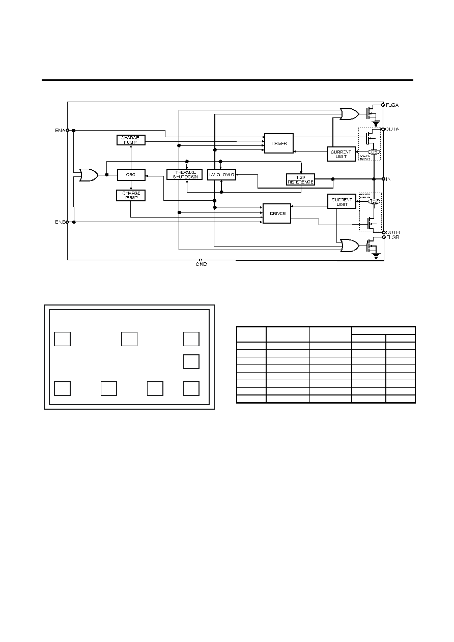
Description
The MIK3526M is a dual integrated high-side power switch with independent enable and flag functions, optimized for self-powered and
bus-powered Universal Serial Bus (USB) applications. The MIK3526M satisfies the following USB requirements: each switch channel
supplies up to 100 mA; the switch's low on-resistance meets USB voltage drop requirements; fault current is limited to typically 250mA,
and a flag output is available to indicate fault conditions to the local USB controller. Additional features include thermal shutdown to
prevent catastrophic switch failure from high-current loads, undervoltage lockout (UVLO) to ensure that the device remains off unless
there is a valid input voltage present, and 3.3V and 5V logic compatible enable inputs. The MIK3526M is available in active-high and
active-low versions in 8-pin DIP and SOIC packages.
Features
∑
2 independent switches
∑
Individual open-drain fault flag pins
∑
2.7V to 5.5V input
∑
100mA continuous load current per port
∑
500m
maximum on-resistance
∑
1µA Maximum Standby Supply Current
∑
Thermal shutdown
∑
Undervoltage lockout (UVLO)
∑
Active-high or active-low enable versions
Applications
∑ USB Power Management
∑ Hot plug-in power supplies
∑ Battery - Charger circuits
Ordering Information
Part Number
Enable
Temperature Range
MIK3526M-H Active
High -40
∞C to +85∞C
MIK3526M-L Active
Low -40
∞C to +85∞C
Pin configuration MIK3526M
-X
8(OUTA)
7(IN)
5(OUTB)
6 (GND)
(ENA) 1
(ENB) 4
(FLGA) 2
(FLGB) 3
LOGIC,
CHARGE
PUMP
LOGIC,
CHARGE
PUMP
Pin Description
Pin
Number
Pin
Name
Pin Function
1, 4
EN(A/B)
Enable (Input): Logic-compatible enable input. High input > 2.1V typical. Low input <1.9V typical (H active
high, L active low).
2, 3
FLG(A/B)
Fault Flag (Output): Active-low, open-drain output. Indicates overcurrent, and thermal shutdown, UVLO,
OVLO.
6 GND
Ground.
7
IN
Supply Input: Output MOSFET drain. Also supplies IC's internal circuitry.
8, 5
OUT(A/B)
Switch Output: Output MOSFET source. Typically connect to switched side of load.
Detailed description
Power switch
The power switch is an N-channel MOSFET with a maximum on-state resistance of 500 m
(V
IN
=5V). The power switch supplies a
minimum of 100 mA per switch.
Enable (EN or EN)
The logic enable disables the power switch and the bias for the charge pump, driver, and other circuitry to reduce the supply current to
less than 1
µA when a logic high is present on EN (MIK3526M-L) or a logic low is present on EN (MIK3526M-H). The enable input is
compatible with both TTL and CMOS logic levels.
Driver
The driver controls the gate voltage of the power switch. To limit large current surges the driver incorporates circuitry that controls the
rise times and fall times of the output voltage.
Charge pump
An internal charge pump supplies power to the driver circuit and provides the necessary voltage to pull the gate of the MOSFET above
the source.
Fault Flag FLG (A/B)
FLG is an N-channel, open-drain MOSFET output. The fault-flag is active (low) for one or more of the following conditions: undervoltage,
current limit, or thermal shutdown. The flag output MOSFET is capable of sinking a 10 mA load to typically 100mV above ground.
Multiple FLG pins may be "wire NORed" to a common pull-up resistor.
Thermal shutdown
An internal thermal-sense circuit shuts off the power switch when the junction temperature rises to approximately 150
∫
C. Hysteresis is
built into the thermal sense circuit.
Page 1 of 3
Replacement of
LM3526M-H/L
MIK3526M-H/L
Dual USB Power Control Switch with
Over-Current/Voltage Protection
June 2001 ≠revised November 2001
Current sense (CS)
A sense FET monitors the current supplied to the load. When an overload or short circuit is encountered, the current-sense circuitry
sends a control signal to the driver. The driver in turn reduces the gate voltage and sends the power FET into its saturation region,
which switches the output into a constant current mode.
Undervoltage lockout
UVLO (undervoltage lockout) prevents the output MOSFET from turning on until V
IN
exceeds approximately 2.3V. In the undervoltage
state, the FLAG will be low. After the switch turns on, if the voltage drops below approximately 2.1V, UVLO shuts off the output
MOSFET and signals fault flag. Undervoltage detection functions only when at least one switch is enabled.
Overvoltage lockout
OVLO (overvoltage lockout) prevents the output MOSET from turniny on if V
IN
exeeds approximately 6.5V. Overvoltage detection
functions only when at least one switch is enabled.
Absolute Maximum Ratings
(Note1)
Parameter Maximum
Units
Supply Voltage (V
IN
) 6
Fault Flag Voltage (V
FLG
) 6
V
Fault Flag Current (I
FLG
) 50
mA
Output Voltage (V
OUT
) 6
V
Output Current (I
OUT
) Internally
Limited
A
Control input (V
EN
)
-0.3 to 12
V
Storage Temperature (T
S
)
-65 to 150
0
C
Operating Ratings
(Note 2)
Parameter MIK3526M
Supply Voltage (V
IN
)
2.7V to 5.5V
Ambient Operating Temperature (T
A
)
-40
0
C to +85
0
C
Electrical Characteristics
T = 25oC, VIN = +5V; unless noted
Parameter Condition
Min
Typ
Max
Units
Note 3, switch off, OUT = open,
0.5
1
Supply Current
Note 3, all switches on, OUT = open,
120
200
µA
Low-to-high transition
2.1
2.4
Enable Input Threshold
High-to-low transition, Note 3
0.8
1.9
V
Enable Input Current
V
EN
= 0V
˜ 5.5V
-0.5
±0.01
0.5
µA
Enable Input Capacitance
1
pF
V
IN
= 5V, I
OUT
=100mA , each switch
400
500
Switch Resistance
V
IN
= 3,3V, I
OUT
=100mA , each switch
500
600
m
Output Turn-On Delay
R
L
=10
, each output
0.5 ms
Output Turn-On Rise Time
R
L
=10
, each output
1 ms
Output Turn off Delay
R
L
=10
, each output
1 20
µs
Output Turn off Fall Time
R
L
=10
, each output
1 20
µs
Output Leakage Current
each output (output disabled)
10
µA
Continuous Load Current
each output
0.1
A
each output (enable into load) V
OUT
=4.0V 0.1
0.25
0.5
Short-Circuit Current Limit
each output (enable into load) V
OUT
=0.1V
0.25
0.5
A
Current-Limit Threshold
Ramped load applied to enabled output, V
OUT
< 4.0 V
0.35
0.55
A
T
J
increasing
135
Over temperature Shutdown
Threshold
T
J
decreasing
125
∞C
V
IN
=5,0V, I
L
=10m¿
10
25
V
IN
=3,3V, I
L
=10mA
11
35
Error Flag Output Resistance
V
IN
=2,7V, I
L
=10mA
12
40
Error Flag Off Current
V
FLAG
=5 V
0.01
1
µA
V
IN
increasing
2.3
UVLO Threshold
V
IN
decreasing
2.1
V
V
IN
increasing
6.5
OVLO Threshold
V
IN
decreasing
6.3
V
Note 1: Exceeding the absolute maximum rating may damage the device.
Note 2: The device is not guaranteed to function outside its operating rating.
Note 3: Off is
0.8V and on is 2.4V for the MIK3526M-H. Off is 2.4V and on is 0.8V for the MIK3526M-L. The enable input has
approximately 200mV of hysteresis.
Page 2 of 3