
MI
KRON
JS
C
∑
ht
t
p
:
//ww
w
.mikron.ru
∑
03 No
v
e
mb
e
r
200
3
MIK371x family
∑
COMPLEMENTARY SWITCH FET DRIVERS
1
DATA SHEET
03 N
OVEMBER
2003
N
O
. 00022
R
EV
1-03
CONTENTS
Page
DESCRIPTION
1
FEATURES
1
PIN CONNECTION AND DESCRIPTION
2
BLOCK DIAGRAM
2
ABSOLUTE MAXIMUM RATINGS
3
ELECTRICAL CHARACTERISTICS
3
TYPICAL CHARACTERISTICS
4
T
IME
RELATIONSHIPS
4
T1 D
ELAY
, T2 D
ELAY
vs. R
T
4
I
CC
vs. S
WITCHING
F
REQUENCY
4
I
CC
VS
. R
T
WITH
O
PPOSITE
R
T
= 50
K
4
T1 D
EADBAND
VS
. T
EMPERATURE
AUX
TO
PWR
5
T2 D
EADBAND
VS
. T
EMPERATURE
PWR
TO
AUX
5
TYPICAL APPLICATIONS
5
T
YPICAL
APPLICATION
WITH
TIMED
DELAYS
5
CONTENTS
Page
U
SING
THE
TIMER
INPUT
FOR
ZERO
-
VOLTAGE
SENSING
5
S
ELF
-
ACTUATED
SLEEP
MODE
WITH
THE
ABSENCE
OF
AN
INPUT
PWM
SIGNAL
. W
AKE
UP
OCCURS
WITH
THE
FIRST
PULSE
WHILE
TURN
-
OFF
IS
DETERMINED
BY
THE
(RTO CTO)
TIME
CONSTANT
5
U
SING
AS
A
COMPLEMENTARY
SYNCHRONOUS
RECTIFIER
SWITCH
DRIVER
WITH
N-
CHANNEL
FET
S
5
S
YNCHRONOUS
RECTIFIER
APPLICATION
WITH
A
CHARGE
PUMP
TO
DRIVE
THE
HIGH
-
SIDE
N
-
CHANNEL
BUCK
SWITCH
5
T
YPICAL
FORWARD
CONVERTER
TOPOLOGY
WITH
ACTIVE
RESET
PROVIDED
BY
THE
MIK3714
DRIVING
AN
N-
CHANNEL
SWITCH
(Q1)
AND
A
P-
CHANNEL
AUXILIARY
SWITCH
(Q2)
5
PHYSICAL DIMENSIONS AND MARKING
DIAGRAMS
6
DIP-8
6
SOP-8
6
ORDERING INFORMATION
6
DESCRIPTION
The MIK3714 and the MIK3715 are two families of high
speed drivers. These are designed to provide drive
waveforms for complementary switches.
Complementary switch configurations are commonly
used in synchronous rectification circuits and active
clamp/reset circuits, which can provide zero voltage
switching. In order to facilitate the soft switching
transitions, independently programmable delays
between the two output waveforms are provided on
these drivers. The delay pins also have true zero
voltage sensing capability which allows immediate
activation of the corresponding switch when zero
voltage is applied. These devices require a PWM-type
input to operate and can be interfaced with
commonly available PWM controllers.
In the MIK3714 series, the AUX output is inverted to
allow driving a P-channel MOSFET. In the MIK3715
series the two outputs are configured in a true
complementary fashion.
FEATURES
∑
Single Input (PWM and TTL Compatible)
∑
High Current Power FET Driver, 1.0A Source/2A
Sink
∑
Auxiliary Output FET Driver, 0.5A Source/1A Sink
∑
Time Delays Between Power and Auxiliary
Outputs Independently Programmable from 50 ns
to 500 ns
∑
Time Delay or True Zero-Voltage Operation
Independently Configurable for Each Output
∑
Switching Frequency to 1MHz
∑
Typical 50 ns Propagation Delays
∑
ENBL Pin Activates 220 µA Sleep Mode
∑
Power Output is Active Low in Sleep Mode
∑
Synchronous Rectifier Driver
REPLACEMENT OF:
UC 3714
UC 3715
MIK371x family
COMPLEMENTARY SWITCH FET DRIVERS
2
Design by Vladimir F.Lityaghin / E-mail: lityaghin@mail.ru / Tel: +7(095)532-64-54
MI
KRON
JS
C
∑
h
ttp
:
/
/www.
m
i
kr
o
n
.
r
u
∑
03 No
v
e
mb
e
r
20
0
3
COMPLEMENTARY SWITCH FET DRIVERS
∑
MIK371x family
PIN
NAME
DESCRIPTION
AUX
The AUX switches immediately at INPUT`
S
rising edge but
waits through the T2 delay after
INPUT
'
S
falling edge before
switching. AUX is capable of sourcing 0.5A and sinking 1.0A
of drive current. See the Time Relationships diagram below
for the difference between the MIK3714 and MIK3715 for
INPUT, MAIN, and AUX. During sleep mode, AUX is inactive
with a high impedance.
ENBL
The ENBL input switches at TTL logic levels (approximately
1.2V), and its input range is from 0V to 20V. The ENBL
input will place the device into sleep mode when it is a
logical low. The current into Vcc during the sleep mode is
typically 220mA.
GND
INPUT
The input switches at TTL logic levels (approximately 1.4V) but the allowable range is from 0V to 20V, allowing
direct connection to most common IC PWM controller outputs. The rising edge immediately switches the AUX
output, and initiates a timing delay, T1, before switching on the PWR output. Similarly, the INPUT falling edge
immediately turns off the PWR output and initiates a timing delay, T2, before switching the AUX output.
It should be noted that if the input signal comes from a controller with FET drive capability, this signal provides
another option. INPUT and PWR provide a delay only at the leading edge while INPUT and AUX provide the delay at
the trailing edge.
PWR
The PWR output waits for the T1 delay after the INPUT`
S
rising edge before switching on, but switches off
immediately at INPUT`
S
falling edge (neglecting propagation delays). This output is capable of sourcing 1A and
sinking 2A of peak gate drive current. PWR output includes a passive, self-biased circuit which holds this pin active
low, when ENBL 0.8V regardless of Vcc's voltage.
T1
A resistor to ground programs the time delay between AUX switch turn-off and PWR turn-on.
T2
This pin functions in the same way as T1 but controls the time delay between PWR turn-off and activation of the
AUX switch.
T1, T2
The resistor on each of these pins sets the charging current on internal timing capacitors to provide independent
time control. The nominal voltage level at each pin is 3V and the current is internally limited to 1mA. The total
delay from INPUT to each output includes a propagation delay in addition to the programmable timer but since the
propagation delays are approximately equal, the relative time delay between the two outputs can be assumed to
be solely a function of the programmed delays. The relationship of the time delay vs. RT is shown in the Typical
Characteristics curves.
Either or both pins can alternatively be used for voltage sensing in lieu of delay programming. This is done by pulling
the timer pins below their nominal voltage level which immediately activates the timer output.
V
CC
The Vcc input range is from 7V to 20V. This pin should be bypassed with a capacitor to GND consistent with peak
load current demands.
This is the reference pin for all input voltages and the return point for all device currents. It carries the full peak
sinking current from the outputs. Any tendency for the outputs to ring below GND voltage must be damped or
clamped such that GND remains the most negative potential.
PIN CONNECTION
AND
DESCRIPTION
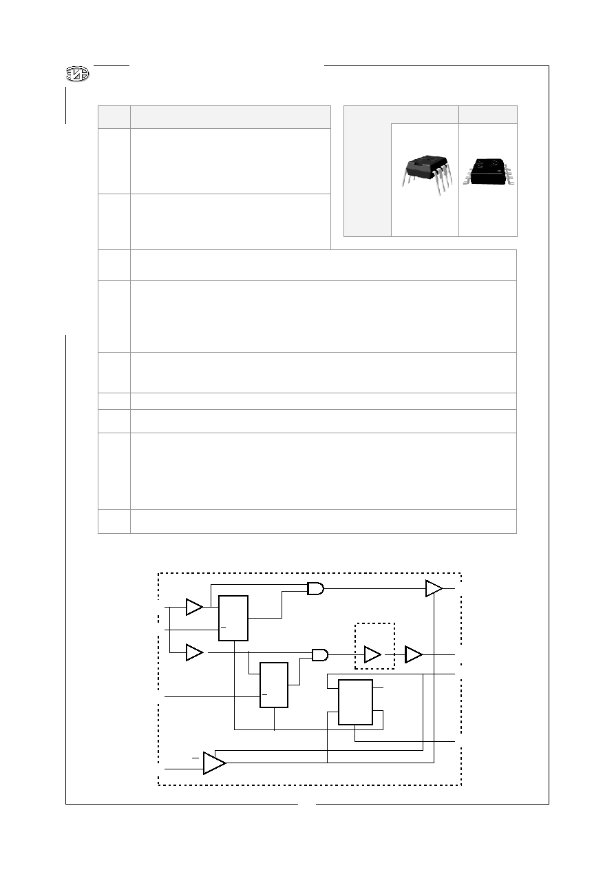
BLOCK DIAGRAM
!
!
!
!
!
!
!
!
!
MIK3714
ONLY
TIMER
LOGIC
GATES
TIMER
REF
GND
AUX
Vcc
PWR
T1
T2
ENBL
1.4V
ENABLE
INPUT
TIMER
6
7
5
8
3
1
4
2
S
S
50ns ˜ 500ns
50ns ˜ 500ns
Q
Q
R
R
V
REF
V
REF
BIAS
Vcc
5V
3V
ENBL
GND
"
"
"
"
"
"
!
!
MIK371x
N
MIK371x
D
1 -- Vcc
2 -- PWR
3 -- GND
4 -- AUX
5 -- T2
6 -- INPUT
7 -- T1
8 -- ENBL
DIP-8
SOP-8
1
4
8
5
8
5
1
4
MI
KRON
JS
C
∑
ht
t
p
:
//ww
w
.mikron.ru
∑
03 No
v
e
mb
e
r
200
3
MIK371x family
∑
COMPLEMENTARY SWITCH FET DRIVERS
3
ABSOLUTE MAXIMUM RATINGS
Note 1: Unless otherwise indicated, voltages are referenced to ground and currents are positive info, negative out of, the
specified terminals.
SYMBOL
PARAMETER
MAXIMUM
UNIT
V
CC
Supply Voltage (low impedance source)
20
V
continuous -200
mA
I
OH
Power Driver
peak -1
A
continuous 400
mA
I
OL
Power Driver
peak 2
A
continuous -100
I
OH
Auxiliary Driver
peak -500
mA
continuous 200
mA
I
OL
Auxiliary Driver
peak 1
A
INPUT, ENBL
Input Voltage Range
-0.3 to 20
V
Storage Temperature Range
-65 to 150
Operating Junction Temperature (Note 1)
150
Lead Temperature (Soldering 10 seconds)
300
o
C
ELECTRICAL CHARACTERISTICS
(V
CC
=15V, ENBL
2V, R
T
1=100k
from T1 to GND, R
T
2=100k
from T2 to GND, and T
A
=0
0
C to +70
0
C,
T
A
= T
J
unless otherwise stated)
SYMBOL CHARACTERISTICS
TEST
CONDITION
MIN
TYP
MAX
UNIT
OVERALL
V
CC
V
CC
7
20
V
I
CC
I
CC
, nominal
ENBL = 2.0V
18
24
mA
I
CC sleep
I
CC
, sleep mode
ENBL = 0.8V
200
300
µA
POWER DRIVER (PWR)
V
OL
Pre
Turn-on
Pre Turn-on PWR Output,
Low
V
CC
= 0V, I
OUT
= 10mA, ENBL= 0.8V
0.3
1.6
INPUT= 0.8V, I
OUT
= 40 mA
0.3
0.8
V
OL
PWR Output Low, Sat.
(V
PWR
)
INPUT= 0.8V, I
OUT
= 400 mA
2.1
2.8
INPUT= 2.0V, I
OUT
= -20 mA
2.1
3
V
OH
PWR Output High,
Sat. (V
CC
-V
PWR
)
INPUT= 2.0V, I
OUT
= -200 mA
2.3
3
V
Tr
Rise Time
C
L
= 2200pF
30
60
Tf
Fall Time
C
L
= 2200pF
25
60
T1 delay
T1 Delay, AUX to PWR
INPUT= rising edge, R
T
1= 10k
(Note 3)
20 35 80
T1 delay
T1 Delay, AUX to PWR
INPUT= rising edge, R
T
1=100k (Note 3)
350 500 700
Tpd
PWR Prop Delay
INPUT falling edge, 50% (Note 2)
35
100
ns
AUXILIARY DRIVER (AUX)
V
IN
= 2.0V, I
OUT
= 20mA
0.3
0.8
V
OL
AUX Output Low, Sat
(V
AUX
)
V
IN
= 2.0V, I
OUT
= 200mA
1.8
2.6
V
IN
= 0.8V, I
OUT
= -10mA
2.1
3.0
V
OH
AUX Output High, Sat
(V
CC
-V
AUX
)
V
IN
= 0.8V, I
OUT
= -100mA
2.3
3.0
V
Tr
Rise Time
C
L
= 1000pF
45
60
Tf
Fall Time
C
L
= 1000pF
30
60
T2 delay
T2 Delay, AUX to PWR
INPUT= rising edge, R
T
2= 10k (Note 3)
20 50 80
T2 delay
T2 Delay, AUX to PWR
INPUT= rising edge, R
T
2=100k (Note 3)
250 350 550
Tpd
AUX Prop Delay
INPUT falling edge, 50% (Note 2)
35
80
ns
Continuation of the table on the next page ...
4
Design by Vladimir F.Lityaghin / E-mail: lityaghin@mail.ru / Tel: +7(095)532-64-54
MI
KRON
JS
C
∑
h
ttp
:
/
/www.
m
i
kr
o
n
.
r
u
∑
03 No
v
e
mb
e
r
20
0
3
COMPLEMENTARY SWITCH FET DRIVERS
∑
MIK371x family
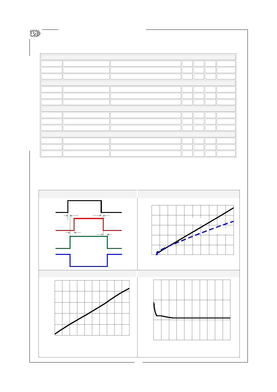
TIME RELATIONSHIPS (
N
OTES
2, 3
)
T1 D
ELAY
, T2 D
ELAY
VS
. R
T
Icc vs. SWITCHING FREQUENCY
I
CC
VS
. R
T
WITH
O
PPOSITE
R
T
= 50
K
RT1 = RT2 = 50k
Duty Cycle = 50%
No Load
TYPICAL CHARACTERISTICS
ELECTRICAL CHARACTERISTICS
(CONTINUED)
(V
CC
=15V, ENBL
2V, R
T
1=100k
from T1 to GND, R
T
2=100k
from T2 to GND, and T
A
=0
0
C to +70
0
C,
T
A
= T
J
unless otherwise stated)
Note 2: Propagation delay times are measured from the 50% point of the input signal to the 10% point of the output signal's
transition with no load on outputs.
Note 3: T1 delay is defined from the 50% point of the transition edge of AUX to the 10% of the rising edge of PWR. T2 delay is
defined from the 90% of the falling edge of PWR to the 50% point of the transition edge of AUX.
ENABLE (ENBL)
Vth
Input
Threshold
0.8 1.2 2.0
V
I
IH
Input Current, I
IH
ENBL = 15V
1
10
µA
I
IL
Input Current, I
IL
ENBL = 0V
-1
-10
µA
T1
I
LIM
Current Limit
T1 = 0V
-1.6
-2
mA
V
T1
Nominal Voltage at T1
2.7
3
3.3
V
TdZVS
Minimum T1 Delay
T1 = 2.5V (Note 3)
40
70
ns
T2
I
LIM
Current Limit
T2 = 0V
-1.2
-2
mA
V
T2
Nominal Voltage at T2
2.7
3
3.3
V
TdZVS
Minimum T2 Delay
T2 = 2.5V (Note 3)
50
100
ns
INPUT (INPUT)
Vth
Input
Threshold
0.8 1.4 2.0
V
I
IH
Input Current, I
IH
INPUT = 15V
1
10
µA
I
IL
Input Current, I
IL
INPUT = 0V
-5
-20
µA
500
400
300
200
100
10
20
30
40
50
60
70
80
90
100
0
R
T
(k )
DE
L
A
Y
(n
s
)
T1
R 1
vs.
T
T2
R 2
vs.
T
16
17
18
19
20
21
100
300
500
700
900
200
400
600
800
1000
0
SWITCHING FREQUENCY (kHz)
Icc
(m
A)
16
17
18
15
10
20
30
40
50
60
70
80
90
100
0
R
T
(k )
Icc
(m
A)
INPUT
PWR OUTPUT
PROPAGATION
DELAYS
T1 DELAY
T2 DELAY
MIK3715
AUX OUTPUT
MIK3714
AUX OUTPUT
MI
KRON
JS
C
∑
ht
t
p
:
//ww
w
.mikron.ru
∑
03 No
v
e
mb
e
r
200
3
MIK371x family
∑
COMPLEMENTARY SWITCH FET DRIVERS
5
TYPICAL CHARACTERISTICS
(CONTINUED)
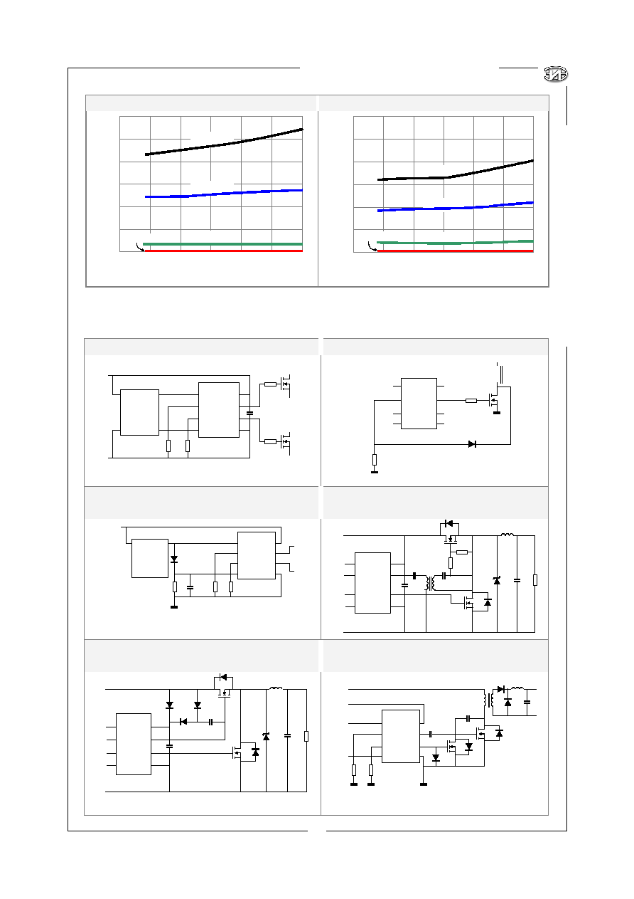
T1 D
EADBAND
VS
. T
EMPERATURE
AUX
TO
PWR
T2 D
EADBAND
VS
. T
EMPERATURE
PWR
TO
AUX
TYPICAL APPLICATION WITH TIMED DELAYS
USING THE TIMER INPUT FOR ZERO-VOLTAGE SENSING
S
ELF
-
ACTUATED
SLEEP
MODE
WITH
THE
ABSENCE
OF
AN
INPUT
PWM
SIGNAL
U
SING
AS
A
COMPLEMENTARY
SYNCHRONOUS
RECTIFIER
SWITCH
DRIVER
WITH
N-
CHANNEL
FET
S
W
AKE
UP
OCCURS
WITH
THE
FIRST
PULSE
WHILE
TURN
-
OFF
IS
DETERMINED
BY
THE
(RTO CTO)
TIME
CONSTANT
S
YNCHRONOUS
RECTIFIER
APPLICATION
WITH
A
CHARGE
PUMP
TO
DRIVE
THE
HIGH
-
SIDE
N
-
CHANNEL
BUCK
SWITCH
T
YPICAL
FORWARD
CONVERTER
TOPOLOGY
WITH
ACTIVE
RESET
PROVIDED
BY
THE
MIK3714
DRIVING
AN
N-
CHANNEL
SWITCH
(Q1)
AND
A
P-
CHANNEL
AUXILIARY
SWITCH
(Q2)
V
IN
is limited to 10V as Vcc will rise to approximately 2V
IN
TYPICAL APPLICATIONS
100
200
300
400
500
600
25
75
50
-25
-75
-50
0
0
TEMPERATURE (∫C)
DE
ADBAN
D DE
L
A
Y
(n
s
)
R 1
T
= 100k
R 1
T
= 50k
R 1
T
= 10k
R 1 <
T
6k
100
200
300
400
500
600
25
75
50
-25
-75
-50
0
0
TEMPERATURE (∫C)
DE
A
DBAND DE
L
A
Y
(n
s)
R 2
T
= 100k
R 2
T
= 50k
R 2
T
= 10k
R 2 <
T
6k
Vcc
Vcc
Vcc
Main
Power
Switch
Auxiliary
ZVS
Switch
Bypass
Capacitor
R 1
T
R 2
T
PWM
AUX
GND
V
REF
GND
GND
PWR
INPUT
ENBL
UC3823
UC3842
MIK3842
etc.
MIK3714/15
T2
T1
∑
∑
∑
∑
∑
∑
∑
∑
!
!
!
!
!
R
T
3V THRESHOLD
PWR
MIK3714/15
T1
∑
∑
∑
Vcc
Vcc
OUT
Vcc
PWM Control
Input Signals
R
T
2
R
T
1
D1
VPWM
R
T
0
50k
C
T
0
0.01µF
AUX
AUX
GND
PWR
PWR
INPUT
ENBL
MIK3714/15
T2
T1
PWM
Controller
∑
∑
∑
∑
∑
∑
∑
∑
!
!
!
#
∑
∑
V
IN
Vcc
C2
C1
RG
L
0
C
0
D0
Q1
Q2
R
L
AUX
GND
GND
PWR
MIK3715
∑
∑
∑
∑
∑
∑
∑
∑
∑
∑
∑
∑
∑
∑
∑
∑
∑
∑
∑
∑
∑
∑
!
!
∑
∑
V
IN
Vcc
C1
L
0
C
0
D0
Q1
Q2
D1
D2
D3
C2
R
L
AUX
GND
GND
PWR
MIK3715
∑
∑
∑
∑
∑
∑
∑
∑
∑
∑
∑
∑
∑
∑
∑
∑
∑
!
!
∑
∑
V
IN
Vcc
PWM
ENABLE
Vcc
R 1
T
L
0
C
0
Q1
Q2
D2
D3
D1
C3
C2
R 2
T
AUX
GND
PWR
INPUT
ENBL
MIK3714
T2
T1
∑
∑
∑
∑
∑
∑
∑
∑
∑
∑
∑
∑
∑
∑
∑
!
!
!
!
!
!