Replacement of
AS431
MIK431
Adjustable Precision Shunt
Regulator
February 1998 - revised September 2002
Description
The MIK431 are three-terminal adjustable shunt regulators with specified thermal stability. The output voltage may be set to any value
between V
ref
(approximately 2.5V) and 36 V with two external resistors. These devices have a typical output impedance of 0.2
. Active
output circuitry provides a very sharp turn-on characteristic, making these devices excellent replacements for zener diodes in many
applications.
Features
∑
Equivalent Full-Range Temperature Coefficient 30
ppm/∞C
∑
Temperature Compensated for Operation Over Full Rated
Operating Temperature Range
∑
Adjustable Output Voltage
∑
Fast Turn-On Response
∑
Sink Current Capability 1mA to 100 mA
∑
Low (0.2
Typ) Dynamic Output Impedance
∑
Low Output Noise
Package information
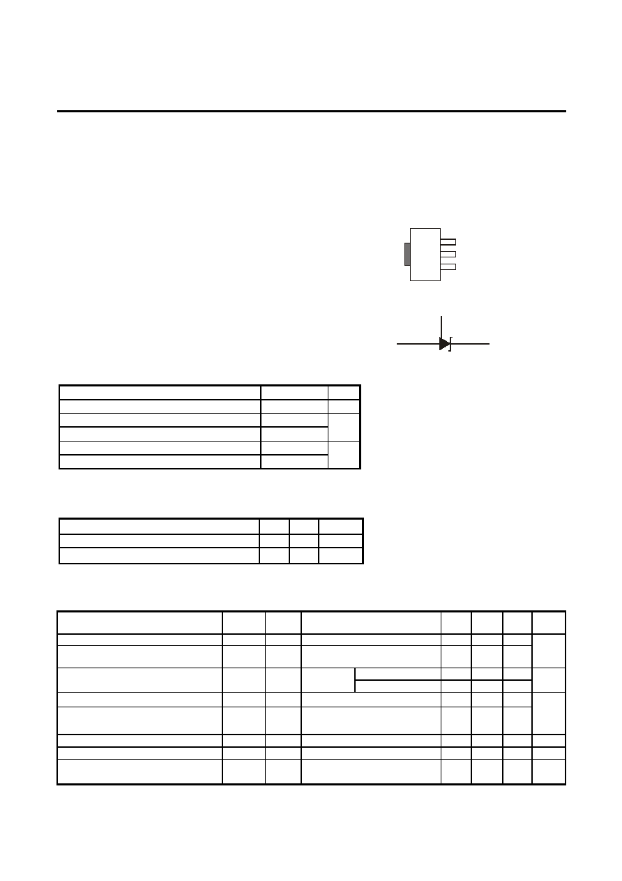
Pin configuration (top view)
SOT-89
CATHODE
ANODE
REF
Symbol
REFERENCE (R)
ANODE
(A)
CATHODE
(K)
Absolute maximum ratings
over operating free-air temperature range (unless otherwise noted)
Parameter Maximum
Units
Cathode voltage (Note 1)
37 V
Continuous cathode current range
-100 to 150
Reference input current range
-50
µA to 10mA
mA
Operating free-air temperature rage
0 to 70
Lead temperature 1.6mm from case for 10 seconds
260
∞C
Note 1: Voltage values are with respect to the anode terminal unless otherwise noted
Recommended operating conditions
Parameter Min
Max
Units
Cathode voltage, V
KA
V
ref
36
V
Cathode current, I
K
(for regulation )
1
100
mA
Electrical characteristics
Electrical characteristics at 25 ∞C free-air temperature(unless otherwise noted)
Parameter Symbol
Test
Circuit
Test Conditions
Min
Typ
Max
Units
Reference input voltage
V
ref
1
V
KA
=V
ref
, l
K
=10mA 2474
2500
2526
Deviation of reference input voltage over
full temperature range
V
ref(dev)
1
V
KA
=V
ref
, l
K
=10mA, T
A
=full range
4
17
mV
V
KA
=10V to V
ref
-2,7 -1.0
Ratio of change in reference input voltage
to the change in cathode voltage
V
ref
/
V
KA
2 l
K
=10mA
V
KA
=36V to 10V
-2 -0.4
mV/V
Reference input current
I
ref
2
l
K
=10mA, R1=10K
, R2=
0.7 4
Deviation of reference input current over
full temperature range
l
ref(dev)
2
l
K
=10mA, R1=10K
, R2=
,
T
A
=full range
0.4
1.2
µA
Minimum cathode current for regulation
I
min
1
V
KA
=V
ref
0.4
1.0
mA
Off-state cathode current
l
off
3
V
KA
=36V, Vref=0
0.1
1
µA
Dynamic impedance
I Z
KA
l
1
V
KA
=V
ref
, l
K
=1mA to 100mA,
f
1KHz
0.2
0.5
Page 1 of 3

Replacement of
AS431
MIK431
Adjustable Precision Shunt
Regulator
February 1998 - revised September 2002
Vref
INPUT
V
KA
I
K
Vref
V
KA
FIGURE 1. TEST CIRCUIT FOR =
Parameter measurement information
Vref
V
KA
FIGURE 2. TEST CIRCUIT FOR >
Vref
Vref
INPUT
V
KA
V
KA
I
K
I
ref
I
ref
R1
R1
R2
( )
∑
+
+
1
R1
R2
=
INPUT
V
KA
I
off
FIGURE 3. TEST CIRCUIT FOR I
off
Typical caracteristics
CATHODE CURRENT
vs
CATHODE VOLTAGE
CATHODE CURRENT
vs
CATHODE VOLTAGE
V - Cathode Voltage (V)
KA
V - Cathode Voltage (V)
KA
I
-
C
a
t
h
o
d
e
C
u
r
r
e
n
t
(
m
A
)
K
150
125
100
75
50
25
0
-25
-50
-75
-100
-2 -1 0 1 2 3
V = V
KA ref
T = 250C
A
I
-
C
a
t
h
o
d
e
C
u
r
r
e
n
t
(
A
)
µ
K
V = V
KA ref
T = 250C
A
80 0
60 0
40 0
20 0
0
-20 0
-1 0 1 2 3
I
min
FIGURE 1
FIGURE 2
Typical applications
FIGURE 2. SINGLE-SUPPLY COMPARATOR WITH
TEMPERATURE-COMPENSATED THRESHOLD
V+
V = 2V
on
V = V+
off
V = 2.5V
(th)
INPUT
OUTPUT
GND
V
out
V
ref
( )
1
R1
R2
=
V+
R1
R2
V
out
V
ref
+
FIGURE 1. SHUNT REGULATOR
Page 2 of 3