Replacement of
LM4558
MIK4558
Dual Wide Bandwidth
Operational Amplifier
November 2001
Description
The MIK4558 devices are dual general-purpose operational amplifiers with each half electrically similar to the
µA741 except that offset
null capability is not provided. The high common-mode input voltage range and the absence of latch-up make these amplifiers ideal for
voltage-follower applications. The devices are short-circuit protected and the internal frequency compensation ensures stability without
external components. The MIK4558 is characterized for operation from 0∞C to 70∞C.
Features
Continuous-Short-Circuit Protection
Wide Common-Mode and Differential
Voltage Ranges
No Frequency Compensation Required
Low Power Consumption
No Latch-Up
Unity-Gain Bandwidth ...3 MHz Typ
Gain and Phase Match Between Amplifiers
Low Noise ...8 nV
Hz
Typ at 1 kHz
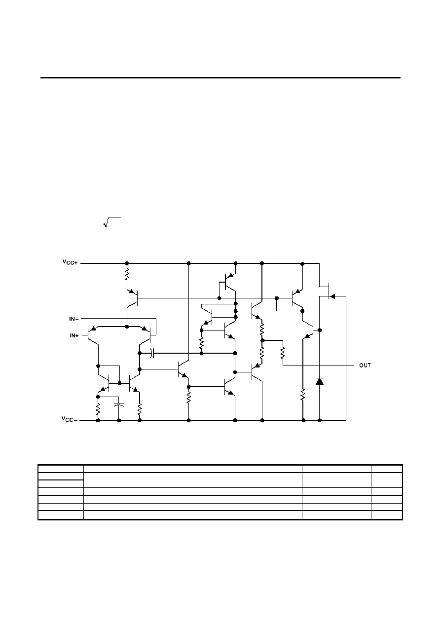
Schematic Diagram
Absolute Maximum Ratings
(unless otherwise noted)
Symbol Parameter
Value
Unit
V
CC
+
V
CC
-
Supply Voltage ≠ (Note 1)
22
-22
V
V
i
Input Voltage ≠ (Note 1, 3)
±15
V
V
id
Differential Input Voltage ≠ (Note 2)
±30
V
Duration of output short circuit to ground, one amplifier at a time (see Note 4)
Unlimited
T
stg
Storage temperature range
-65 to 150
0
C
Note 1: All voltage values, unless otherwise noted, are with respect to the midpoint between V
CC
+ and V
CC
-.
Note 2: Differential voltages are at IN+ with respect to IN ≠.
Note 3: The magnitude of the input voltage must never exceed the magnitude of the supply voltage or 15 V, whichever is less.
Note 4: Temperature and/or supply voltages must be limited to ensure that the dissipation rating is not exceeded.
Page 1 of 3

Replacement of
LM4558
MIK4558
Dual Wide Bandwidth
Operational Amplifier
November 2001
Recommended Operating Conditions
Parameter
Symbol Min Max
Units
V
CC
+ 5 15
Supply voltage
V
CC
- -5 -15
V
Operating free-air temperature
T
A
0 70
∞C
Electrical characteristics
at specified free-air temperature, V
CC
+ = 15 V, V
CC
≠ = ≠15 V (Wafer Form)
MIK4558
Parameter Test
conditions
Min
Typ
Max
Units
25∞C
0.5
5
V
IO
Input offset voltage
V
O
= 0
Full range
6
mV
25∞C
5
200
I
IO
Input offset current
V
O
= 0
Full range
500
nA
25∞C
140
500
I
IB
Input bias current
V
O
= 0
Full range
1500
nA
V
ICR
Common-mode input voltage range
25∞C
±12
±14
V
R
L
= 10 k
25∞C
±12
±14
R
L
= 2 k
25∞C
±10
±13
V
OM
Maximum output voltage swing
R
L
2 k
Full range
±10
V
25∞C 50
350
A
VD
Large signal differential voltage amplification
R
L
2 k
V
O
=
±10 V
Full range
25
V/mV
r
j
Input resistance
25∞C
0.3
5
M
CMRR
Common-mode rejection ratio
25∞C
70
90
dB
k
SVS
Supply-voltage sensitivity (
V
IO
/
V
CC
)
25∞C
30
150
µV/V
25∞C
2.5
5.6
T
A
(min)
3
6.6
I
CC
Supply current (both amplifiers)
V
O
= 0,
No load
T
A
(max)
2
5
mA
Open loop
R
S
=100
85
V
01
/V
02
Crosstalk
attenuation
A
VD
=100
f= 1kHz
25∞C
105
All characteristics are measured under open-loop conditions with zero common-mode input voltage unless otherwise specified. Full
range is 0∞C to 70∞C. T
A
(min) = 0∞C. T
A
(max) = 70∞C.
Page 2 of 3