MI
K
R
ON J
S
C
∑
ht
t
p
://www.m
i
k
r
o
n
.
r
u
∑
19 N
o
v
e
m
b
er 2003
MIK494
∑
PULSE-WIDTH-MODULATION CONTROLLER
1
DATA SHEET
19 N
OVEMBER
2003
N
O
. 00024
R
EV
1-03
CONTENTS
Page
DESCRIPTION
1
FEATURES
1
SCHEMATIC DIAGRAM
2
PIN DESCRIPTION
2
FUNCTIONAL BLOCK DIAGRAM
2
ABSOLUTE MAXIMUM RATINGS
2
RECOMMENDED OPERATING CONDITIONS
2
ELECTRICAL CHARACTERISTICS
3
REFERENCE SECTION
4
OSCILLATOR SECTION
4
AMPLIFIER SECTION
4
OUTPUT SECTION
4
DEAD-TIME CONTROL SECTION
4
CONTENTS
Page
PWM COMPARATOR SECTION
4
TOTAL DEVICE
4
SWITCHING CHARACTERISTICS
4
TEST CIRCUITS
4
PULSE WIDTH MODULATED STEP≠DOWN
CONVERTER
5
PULSE WIDTH MODULATED PUSH≠PULL
CONVERTER
5
APPLICATION INFORMATION
6
PHYSICAL DIMENSIONS and MARKING
DIAGRAMS
7
DIP-16
7
SOP-16
7
ORDERING INFORMATION
8
TYPICAL APPLICATIONS
5
DESCRIPTION
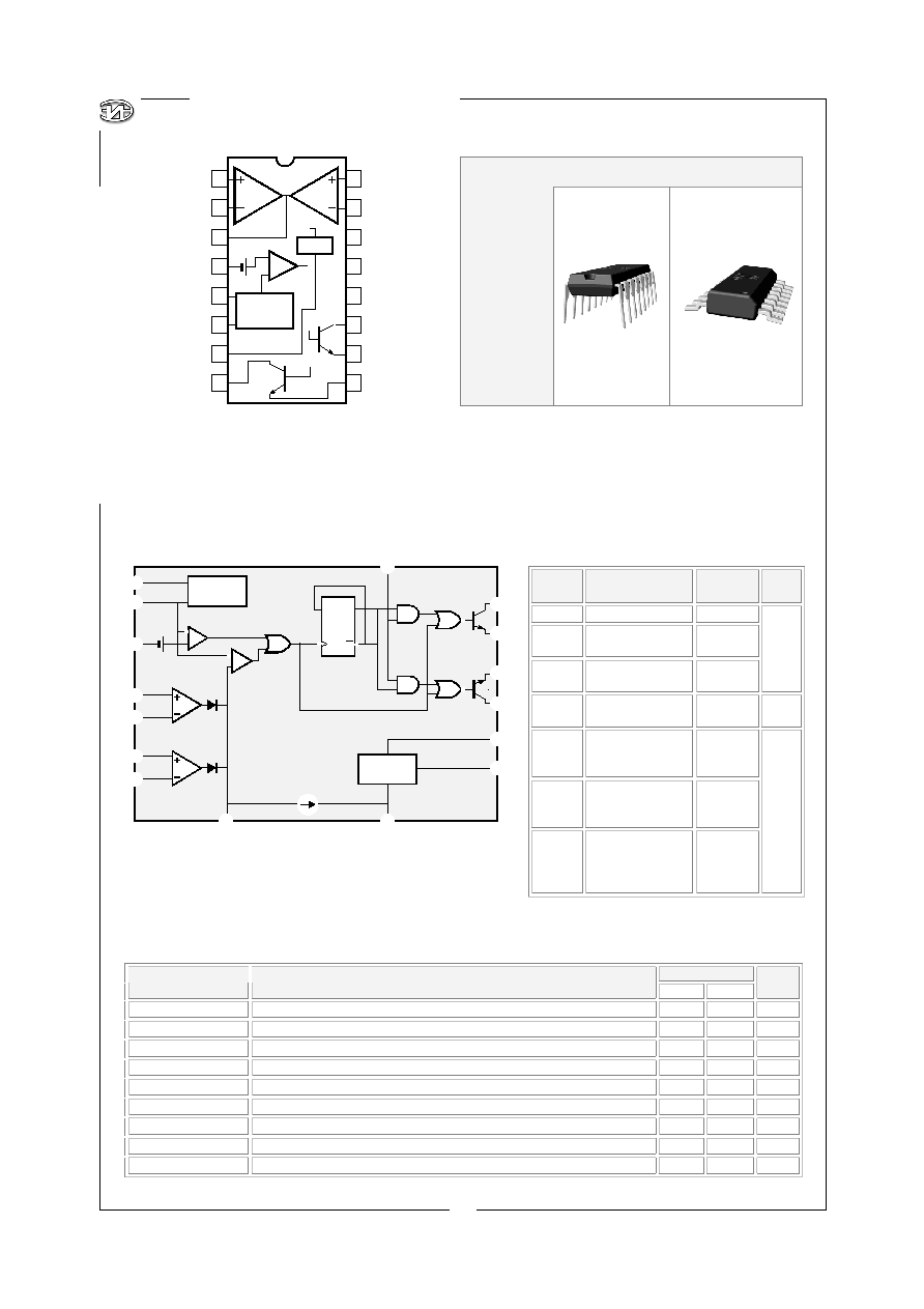
The MIK494 incorporate on a single monolithic chip
all the functions required in the construction of a
pulse-width-modulation control circuit. Designed
primarily for power supply control, these devices
offer the systems engineer the flexibility to tailor
the power supply control circuitry to his
application.
The MIK494 contains an error amplifier, an on-chip
adjustable oscillator, a dead-time control
comparator, pulse-steering control flip-flop, a 5-
volt, 5% precision regulator, and output-control
circuits. The error amplifier exhibits a common-
mode voltage range from -0.3 volts to V
CC
-2 volts.
The dead-time control comparator has a fixed
offset that provides approximately 5% dead time
when externally altered. The on-chip oscillator
may be bypassed by terminating R
T
(pin 6) to the
reference output and providing a sawtooth input
to C
T
(pin 5), or it may be used to drive the
common circuits in synchronous multiple-rail
power supplies. The uncommitted output
transistors provide either common-emitter or
emitter-follower output capability. Each device
provides for push-pull or single-ended output
operation, which may be selected through the
output-control function. The architecture of these
devices prohibits the possibility of either output
being pulsed twice during push-pull operation.
FEATURES
∑
Complete PWM Power Control Circuitry
∑
Uncommitted Outputs for 200 mA Sink or
Source Current
∑
Output Control Selects Single-Ended or Push-
Pull Operation
∑
Internal Circuitry Prohibits Double Pulse at
Either Output
∑
Variable Dead-Time Provides Control over
Total Range
∑
Internal Regulator Provides a Stable
5-V Reference Supply, 5%
∑
Circuit Architecture Allows Easy
Synchronization
REPLACEMENT OF:
TL 494
MIK494
PULSE WIDTH MODULATION CONTROLLER
-
-

2
Design by Vladimir F.Lityaghin / E-mail: lityaghin@mail.ru / Tel: +7(095)532-64-54
MI
K
R
ON J
S
C
∑
ht
t
p
://www.m
i
k
r
o
n
.
r
u
∑
19 N
o
v
e
m
b
er 2003
PULSE-WIDTH-MODULATION CONTROLLER
∑
MIK494
PIN DESCRIPTION
ERROR
AMPLIFIER
ERROR
AMPLIFIER
1
1
NONINVERTING
INPUT
NONINVERTING
INPUT
INVERTING
INPUT
INVERTING
INPUT
DEAD-TIME
CONTROL
FEEDBACK
GROUND
OUTPUT
CONTROL
V
REF
Vcc
C2
E2
E1
C1
C
T
R
T
16
2
15
3
14
4
13
5
12
6
11
7
10
8
Q1
Q2
Vcc
9
2
5V REF
0.1V
OSCILLATOR
MIK494
CN
MIK494
CD
0
1 -- 1 IN+
0
2 -- 1 IN-
0
3 -- FBACK
0
4 -- DTC
0
5 -- C
T
0
6 -- R
T
0
7 -- GND
0
8 -- C1
0
9 -- E1
10 -- E2
11 -- C2
12 -- Vcc
13 -- OUTCTRL
14 -- REF
15 -- 2 IN-
16 -- 2 IN+
DIP-16
SOP-16
1
8
9
16
1
8
9
16
SCHEMATIC DIAGRAM
ABSOLUTE MAXIMUM
RATINGS
(Full operating ambient temperature range applies,
unless otherwise noted.)
VALUE
SYMBOL
PARAMETER
MIN MAX
UNIT
V
CC
Supply voltage
7
40
V
V
IN
Amplifier input voltage
-0.3
V
CC
-2
V
OUT
Collector output voltage
40
I
OUT1
, I
OUT2
Collector output current (each transistor)
200
mA
Current into feedback terminal
0.3
C
T
Timing capacitor
0.47
10000
nF
R
T
Timing resistor
1.8
500
k
f
OSC
Oscillator frequency
1
300
kHz
T
A
Operating free-air temperature
0
70
∞C
RECOMMENDED OPERATING CONDITIONS
FUNCTIONAL BLOCK DIAGRAM
SYMBOL
RATING
VALUE
UNIT
V
CC
Supply voltage
41
V
IN
Amplifier input
voltage
V
CC
+ 0.3
V
OUT
Collector output
voltage
41
V
I
OUT
Collector output
current
250 mA
T
A
Operating free-
air temperature
range
0 to 70
T
STG
Storage
temperature
range
-65 to
150
T
LEAD
Lead
temperature 1,6
mm from case
for 10 seconds
260
∞C
OSCILLATOR
1 IN+
DTC
C
T
R
T
1 IN-
2 IN+
2 IN-
FEEDBACK
!
!
!
11
!
10
!
!
!
!
!
!
!
!
!
!
!
!
!
REFERENCE
REGULATOR
0.7mA
ERROR
AMPLIFIER
1
ERROR
AMPLIFIER
2
PWM
COMPARATOR
PULSE-STEERING
FLIP-FLOP
OUTPUT CONTROL
Q1
C1
C2
Vcc
GND
V
REF
E1
E2
Q2
DEAD-TIME CONTROL
COMPARATOR
D
Q
Q
8
9
12
14
7
13
6
5
4
1
2
16
15
3
C
0.1V
!
!
!
!
!
!
"
"
"
"
"
"
"
"
"
"
"
"

MI
K
R
ON J
S
C
∑
ht
t
p
://www.m
i
k
r
o
n
.
r
u
∑
19 N
o
v
e
m
b
er 2003
MIK494
∑
PULSE-WIDTH-MODULATION CONTROLLER
3
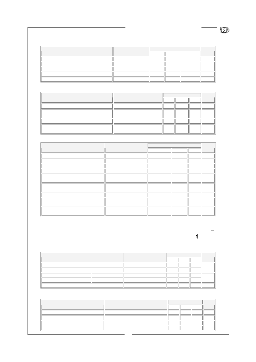
ELECTRICAL CHARACTERISTICS
(Vcc = 15 V, C
T
= 0.01 µF, R
T
= 12 k
, unless otherwise noted.)
REFERENCE SECTION
VALUE
PARAMETER
TEST CONDITIONS *
MIN TYP
** MAX
UNIT
Output voltage (V
ref
)
l
OUT
= 1mA
4.75
5
5.25
V
Input regulation
V
CC
= 7V to 40V
2
25
Output regulation
I
OUT
= 1mA to 10mA
1
15
mV
Output voltage change with temperature
T
A
= MIN to MAX
0.2 1 %
Short-circuit output current ***
V
REF
= 0
35
mA
AMPLIFIER SECTION
(SEE FIGURE 2)
VALUE
PARAMETER
TEST CONDITIONS
MIN TYP
** MAX
UNIT
Input offset voltage
V
OUT
(pin 3) = 2.5V
2
10
mV
Input offset current
V
OUT
(pin 3) = 2.5V
25
250
nA
Input bias current
V
OUT
(pin 3) = 2.5V
0.2
1
µA
Common-mode input voltage range
V
CC
= 7V to 40V
-0.3 to V
CC
-2
V
Open-loop voltage amplification
V
OUT
= 3V, R
L
= 2k,
V
OUT
= 0.5 to 3.5V
70 95
dB
Unity-gain bandwidth
V
OUT
= 0.5 to 3.5V,
R
L
= 2k
800
kHz
Common-mode rejection ratio
V
OUT
= 40V, T
A
= 25∞C
65 80
dB
Output sink current (pin 3)
V
ID
= -15mV to -5V,
V
(pin3)
= 0.7 V
0.3 0.7
mA
Output source current (pin 3)
V
ID
= 15mV to 5V,
V
(pin3)
= 3.5 V
-2
mA
OSCILLATOR SECTION
(SEE FIGURE 1)
VALUE
PARAMETER
TEST CONDITIONS *
MIN TYP
** MAX
UNIT
Frequency
C
T
= 0.01 µF, R
T
= 12k
10 kHz
Standard deviation of frequency ****
All values of V
CC
, C
T
, R
T
, and
T
A
constant
10
%
Frequency change with voltage
V
CC
= 7V to 40V, T
A
= 25∞C
0.1
%
Frequency change with temperature *****
C
T
= 0.01 µF, R
T
= 12k,
T
A
= MIN to MAX
1
%
*
For conditions shown as MIN or MAX, use the appropriate value specified under recommended operating conditions.
**
All typical values except for parameter changes with temperature are at T
A
= 25 ∞C
***
Duration of the short-circuit should not exceed one second
****
Standard deviation Is a measure of the statistical distribution about the mean as derived from the formula:
*****
Temperature coefficient of timing capacitor and timing resistor not taken Into account
(
)
1
1
2
-
-
=
=
N
n
X
x
N
n
OUTPUT SECTION
VALUE
PARAMETER
TEST CONDITIONS
MIN TYP
* MAX
UNIT
Collector off-state current
V
CE
= 40V, V
CC
= 40V
2
100
Emitter off-state current
V
CC
= V
C
= 40V, V
E
= 0
-100
µA
Collector-emitter saturation
Common-emitter
V
E
= 0, I
C
= 200 mA
1.1
1.3
voltage Emitter-follower
V
C
= 15V, I
E
= -200 mA
1.5
2.5
V
Output control input current
V
IN
= V
REF
3.5
mA
DEAD-TIME CONTROL SECTION
(SEE FIGURE 1)
VALUE
PARAMETER
TEST CONDITIONS
MIN TYP
* MAX
UNIT
Input bias current (pin 4)
V
IN
= 0 to 5.25V
-2
-10
µA
Maximum duty cycle, each output
V
IN
(pin 4)
= 0, C
T
= 0.1µF, R
T
= 12k
45 %
Zero duty cycle
3
3.3
Input threshold voltage (pin 4)
Maximum duty cycle
0
V

4
Design by Vladimir F.Lityaghin / E-mail: lityaghin@mail.ru / Tel: +7(095)532-64-54
MI
K
R
ON J
S
C
∑
ht
t
p
://www.m
i
k
r
o
n
.
r
u
∑
19 N
o
v
e
m
b
er 2003
PULSE-WIDTH-MODULATION CONTROLLER
∑
MIK494
ELECTRICAL CHARACTERISTICS
(CONTINUED)
Vcc = 15 V, C
T
= 0.01 µF, R
T
= 12 k
, unless otherwise noted.
PWM COMPARATOR SECTION
(SEE FIGURE 1)
VALUE
PARAMETER
TEST CONDITIONS
MIN TYP
* MAX
UNIT
Input threshold voltage (pin 3)
Zero duty cycle
4
4.5
V
Input sink current (pin 3)
V
(pin 3)
= 0.7V
0.3
0.7
mA
TOTAL DEVICE
VALUE
PARAMETER
TEST CONDITIONS
MIN TYP
* MAX
UNIT
V
CC
= 15V
--
6
10
Standby supply current
Pin 6 at V
REF
, all other inputs and
outputs open
V
CC
= 40V
--
9
15
Average supply current
V
IN (pin 4)
= 2V, See Figure 1
--
7.5
--
mA
* AII typical values except for temperature coefficient are at T
A
=25
∞
C
SWITCHING CHARACTERISTICS
VALUE
PARAMETER
TEST CONDITIONS
MIN TYP
* MAX
UNIT
Output voltage rise time
100
200
Output voltage fall time
Common-emitter configuration. See Figure 3
25
100
Output voltage rise time
100
200
Output voltage fall time
Emitter-follower configuration. See Figure 4
40
100
ns
DTC
C1
150
2W
50k
12k
0.01µF
150
2W
E1
C2
E2
REF
GND
Vcc
Vcc=15V
OUTPUT 1
OUTPUT 2
TEST
INPUTS
FEEDBACK
OUTPUT
CTRL
R
T
R
T
C
T
C
T
1 IN+
2 IN+
2 IN-
1 IN-
"
"
"
"
"
"
"
"
!
!
!
!
!
!
!
!
!
!
!
14
10
12
!
13
!
15
!
16
11
9
8
4
3
6
5
!
1
!
2
7
D
C
EADTIME
ONTROL
D
C
UTY
YCLE
MAX
0%
0%
V
at C1
OLTAGE
Vcc
Vcc
0V
0V
0V
0.7V
V
at C2
OLTAGE
FEEDBACK
V
at C
OLTAGE
T
T
HRESHOLD
VOLTAGE
T
HRESHOLD
VOLTAGE
EACH
OUTPUT
CIRCUIT
OUTPUT
TEST CIRCUIT
OUTPUT VOLTAGE WAVEFORM
C
L
C
L
=15 F (
)
p
INCLUDES
PROBE
AND
JIG
CAPACITANCE
t
F
t
R
90%
90%
10%
10%
15V
68
2W
"
"
"
EMITTER--FOLLOWER CONFIGURATION
FIGURE 4
EACH
OUTPUT
CIRCUIT
OUTPUT
TEST CIRCUIT
OUTPUT VOLTAGE WAVEFORM
C
L
C
L
=15 F (
)
p
INCLUDES
PROBE
AND
JIG
CAPACITANCE
t
F
t
R
90%
90%
10%
10%
15V
68
2W
"
"
"
COMMON--EMITTER CONFIGURATION
FIGURE 3
ERROR AMPLIFIER
UNDER TEST
OTHER
ERROR AMPLIFIER
FEEDBACK
TERMINAL
(PIN 3)
!
!
!
!
!
!
"
V
IN
V
REF
ERROR AMPLIFIER CHARACTERISTICS
FIGURE 2
OPERATIONAL TEST CIRCUIT AND VOLTAGE WAVEFORMS
FIGURE 1

MI
K
R
ON J
S
C
∑
ht
t
p
://www.m
i
k
r
o
n
.
r
u
∑
19 N
o
v
e
m
b
er 2003
MIK494
∑
PULSE-WIDTH-MODULATION CONTROLLER
5
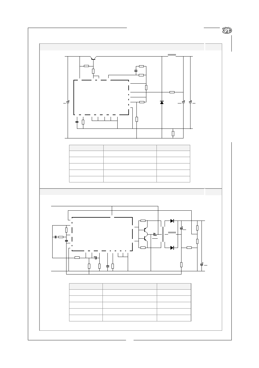
TYPICAL APPLICATIONS
PULSE WIDTH MODULATED STEP≠DOWN CONVERTER
PULSE WIDTH MODULATED PUSH≠PULL CONVERTER
FIGURE 5
FIGURE 6
TEST
CONDITION
RESULTS
Line Regulation
V
IN
= 8.0V to 40V
3
mV 0.01%
Load Regulation
V
IN
= 12.6V, I
OUT
= 0.2mA to 200mA
5
mV 0.02%
Output Ripple
V
IN
= 12.6V, I
OUT
= 200mA
40
mV pp P.A.R.D.
Short Circuit Current
V
IN
= 12.6V, R
L
= 0.1
250
mA
Efficiency
V
IN
= 12.6V, I
OUT
= 200mA
72
%
TEST
CONDITION
RESULTS
Line Regulation
V
IN
= 8.0V to 40V
3
mV 0.01%
Load Regulation
V
IN
= 12.6V. I
OUT
= 0.2mA to 200mA
5
mV 0.02%
Output Ripple
V
IN
= 12.6 V, I
OUT
= 200mA
40
mV pp P.A.R.D.
Short Circuit Current
V
IN
= 12.6V, R
L
= 0.1
250
mA
Efficiency
V
IN
= 12.6V I
OUT
= 200mA
72
%
!!!!
C
T
+V
IN
= 10V to 40V
+V
OUT
= 5V
I
OUT
= 1A
R
T
MIK 494
DTC
Vcc
C1
C2
FBACK
1IN-
2IN-
2IN+
1IN+
REF
E1
E2
5.1k
150
500
10V
All capacitors in µF
50
10V
50
10V
KSA1010
MR850
5.1k
5.1k
0.1
0.1
1M
47k
1mH, 2A
47
47k
150
0.01
O
U
TC
TR
L
GND
!
16
!
15
!
14
!
1
!
2
!
3
!
12
!
8
!
5
!
7
"
"
"
"
"
"
"
"
"
"
"
"
"
"
"
"
"
"
!
10
!
9
!
13
!
4
!
6
!
11
"
"
"
"
"
"
"
"
"
!
!
!
!
!
!
!
!
!
!
!
!
!
!
!
!
!
!
!
! !!!!
C
T
+V
IN
= 8V to 20V
+V
OUT
= 28V
I
OUT
= 0.2A
R
T
MIK 494
DTC
Vcc
C1
C2
FBACK
1IN-
2IN-
2IN+
1IN+
REF
E1 E2
50
35V
50
35V
50µF
25V
All capacitors in µF
240
15k
47
22k
1N4934
3.5mH,
0.3A
T1
1N4934
47
4.7k
4.7k
4.7k
10k
10
1M
33k
15
0.01
1.0
0.001
O
U
TC
TR
L
GND
!
16
!
15
!
14
!
1
!
2
!
3
!
12
!
8
!
5
!
7
"
"
"
"
"
"
"
"
"
"
"
"
"
"
"
"
"
"
"
"
"
"
"
"
"
"
"
"
"
"
"
"
"
"
"
"
"
"
"
"
!
10
!
9
!
13
!
4
!
6
!
11
!
!
!
!

6
Design by Vladimir F.Lityaghin / E-mail: lityaghin@mail.ru / Tel: +7(095)532-64-54
MI
K
R
ON J
S
C
∑
ht
t
p
://www.m
i
k
r
o
n
.
r
u
∑
19 N
o
v
e
m
b
er 2003
PULSE-WIDTH-MODULATION CONTROLLER
∑
MIK494
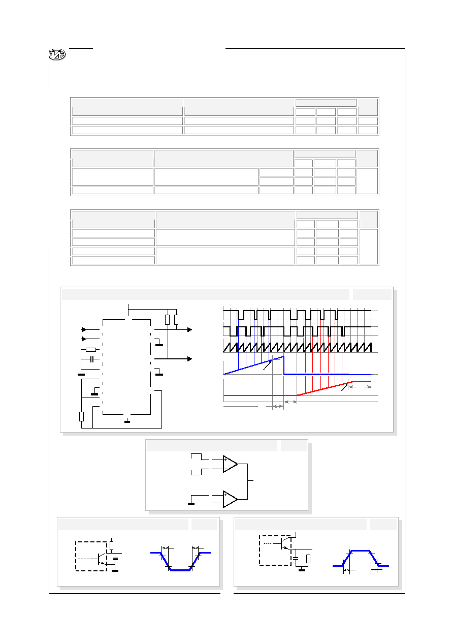
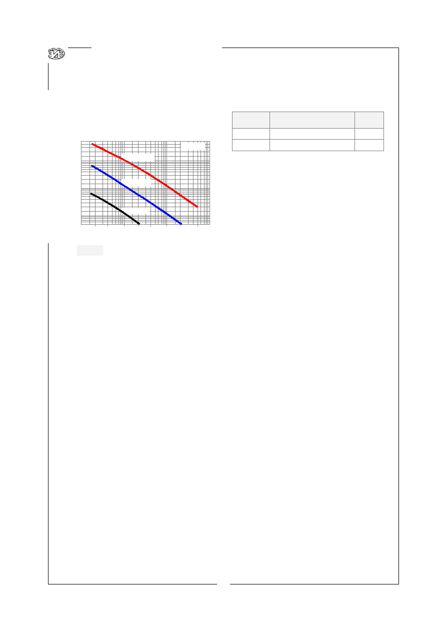
The MIK494 is a fixed≠frequency pulse width modulation
control circuit, incorporating the primary building blocks
required for the control of a switching power supply.
(See Figure 1.) An internal≠linear sawtooth oscillator is
frequency≠programmable by two external components,
R
T
and C
T
.
For more information refer to Figure 7.
Output pulse width modulation is accomplished by
comparison of the positive sawtooth waveform across
capacitor C
T
to either of two control signals. The NOR
gates, which drive output transistors Q1 and Q2, are
enabled only when the flip≠flop clock≠input line is in its
low state. This happens only during that portion of time
when the sawtooth voltage is greater than the control
signals. Therefore, an increase in control≠signal
amplitude causes a corresponding linear decrease of
output pulse width. (Refer to the Timing Diagram shown
in Figure 1.)
The control signals are external inputs that can be fed
into the deadtime control, the error amplifier inputs, or
the feedback input. The deadtime control comparator
has an effective 120 mV input offset which limits the
minimum output deadtime to approximately the first 4%
of the sawtooth≠cycle time. This would result in a
maximum duty cycle on a given output of 96% with the
output control grounded, and 48% with it connected to
the reference line.
Additional deadtime may be imposed on the output by
setting the deadtime≠control input to a fixed voltage,
ranging between 0 V to 3.3 V.
The pulse width modulator comparator provides a means
for the error amplifiers to adjust the output pulse width
from the maximum percent on≠time, established by the
deadtime control input, down to zero, as the voltage at
the feedback pin varies from 0.5 V to 3.5 V. Both error
amplifiers have a common mode input range from ≠0.3 V
to (VCC ≠ 2V), and may be used to sense power≠supply
output voltage and current. The error≠amplifier outputs
are active high and are ORed together at the
noninverting input of the pulse≠width modulator
comparator. With this configuration, the amplifier that
demands minimum output on time, dominates control of
the loop.
When capacitor C
T
is discharged, a positive pulse is
generated on the output of the deadtime comparator,
which clocks the pulse≠steering flip≠flop and inhibits the
output transistors, Q1 and Q2. With the output≠control
connected to the reference line, the pulse≠steering flip≠
flop directs the modulated pulses to each of the two
output transistors alternately for push≠pull operation.
The output frequency is equal to half that of the
oscillator. Output drive can also be taken from Q1 or Q2,
when single≠ended operation with a maximum on≠time of
less than 50% is required. This is desirable when the
output transformer has a ringback winding with a catch
diode used for snubbing. When higher output≠drive
currents are required for single≠ended operation, Q1 and
Q2 may be connected in parallel, and the output≠mode
pin must be tied to ground to disable the flip≠flop. The
output frequency will now be equal to that of the
oscillator.
The MIK494 has an internal 5.0V reference capable of
sourcing up to 10 mA of load current for external bias
circuits. The reference has an internal accuracy of ±5.0%
with a typical thermal drift of less than 50mV over an
operating temperature range of 0∞ to 70∞C.
APPLICATION INFORMATION
C
T
= 0.001µF
V
CC
= 15V
C
T
= 0.01µF
C
T
= 0.1µF
500k
100k
10k
500
1k
1k
2k
5k
10k
20k
50k
100k 200k
500k 1M
R -- TIMING RESISTANCE
T
( )
f
OS
C
-- O
S
CIL
L
A
T
O
R F
R
E
Q
UE
NCY
(H
)
z
FIGURE 7
Oscillator Frequency versus Timing
Resistance
INPUT/OUTPUT
CONTROLS
OUTPUT FUNCTION
f
OUT
/f
OSC
=
Grounded
Single≠ended PWM @ Q1 and Q2
1.0
@ Vref
Push≠pull Operation
0.5
FUNCTIONAL TABLE

MI
K
R
ON J
S
C
∑
ht
t
p
://www.m
i
k
r
o
n
.
r
u
∑
19 N
o
v
e
m
b
er 2003
MIK494
∑
PULSE-WIDTH-MODULATION CONTROLLER
7
A
B
C
D
E
F
G
H J K
L
A
B
C
D
E
F
G H J
K
L
1
8
9
16
H
45∫
x
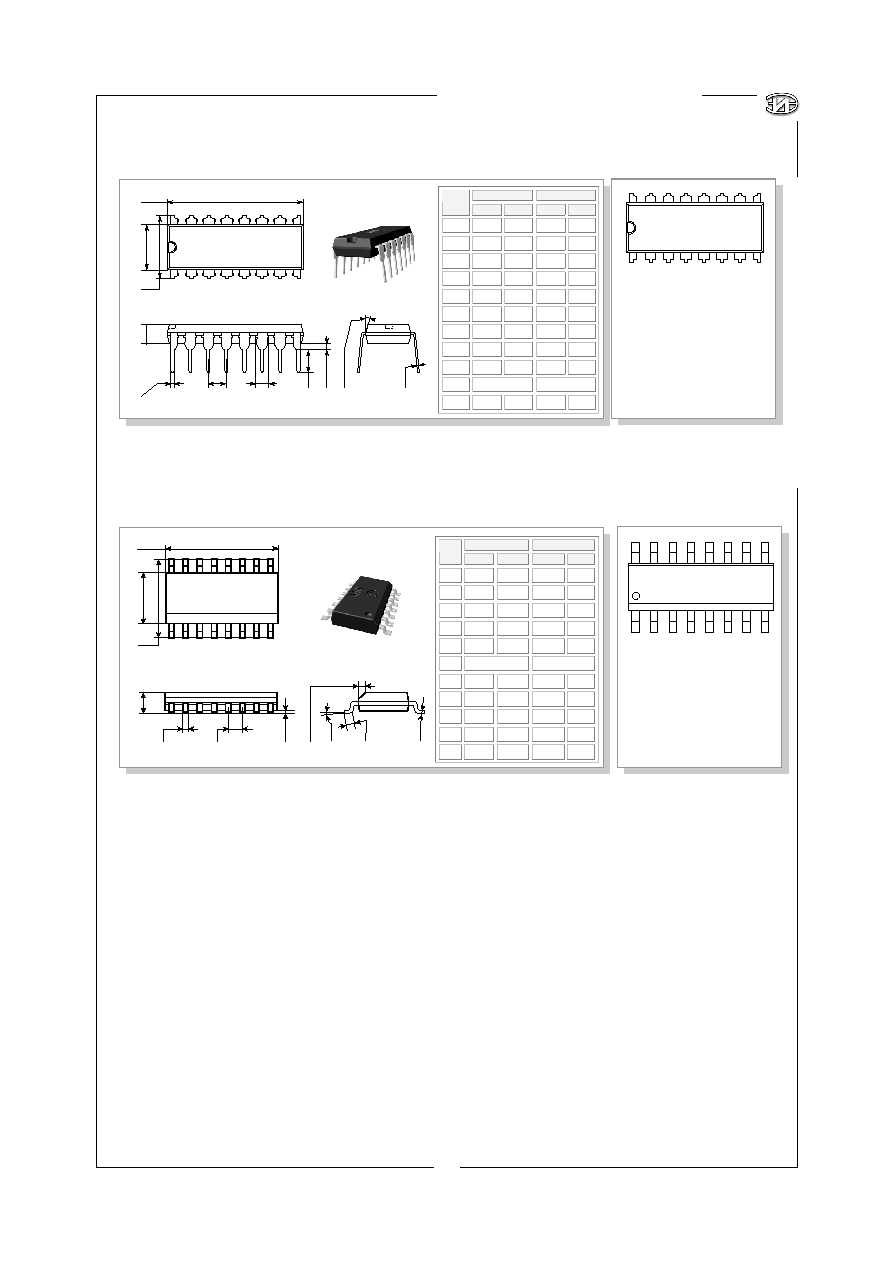
PHYSICAL DIMENSIONS
AND
MARKING DIAGRAMS
SOP-16
PACKAGE
SOP-16
MARKING DIAGRAM
DIP-16
PACKAGE
DIP-16
MARKING DIAGRAM
MIK494
YYWW/n
YY -- Year
WW -- Work Week
n -- Assembly Location
MIK494
YYWW/n
YY -- Year
WW -- Work Week
n -- Assembly Location
MILLIMETERS
INCHES
POS
Min
Max
Min
Max
A
9.80 10.00 0.386 0.393
B
3.80 4.00 0.150
0.157
C
5.80 6.20 0.229
0.244
D
1.35 1.75 0.054
0.068
E
0.35 0.49 0.014
0.019
F
1.27 BSC
0.05 BSC
G
0.10 0.25 0.004
0.009
H
0.25 0.50 0.010
0.019
J
0∫ 7∫ 0∫ 7∫
K
0.40 1.25 0.016
0.049
L
0.19 0.25 0.008
0.009
MILLIMETERS
INCHES
POS.
MIN
MAX
MIN
MAX
A
19,50 19,60 0,768 0,772
B
6,30
6,40 0,248 0,252
C
8,30
9,30 0,327 0,366
D
3,15
3,35 0,124 0,132
E
0,41
0,51 0,016 0,020
F
2,49
2,59 0,098 0,102
G
-- 1,82
-- 0,072
H
3,00
3,50 0,118 0,138
J
0,50
1,10 0,020 0,043
K
13∫ 13∫
L
0,20
0,30 0,008 0,012
1
8
9
16
1
8
9
16

8
Design by Vladimir F.Lityaghin / E-mail: lityaghin@mail.ru / Tel: +7(095)532-64-54
MI
K
R
ON J
S
C
∑
ht
t
p
://www.m
i
k
r
o
n
.
r
u
∑
19 N
o
v
e
m
b
er 2003
PULSE-WIDTH-MODULATION CONTROLLER
∑
MIK494
!
Address: 1
ST
Zapadny Proezd 12, Building 1, Zelenograd, Moscow, Russia, 124460
"
Telephone: +7 (095) 535-23-43; 536-85-44
#
Fax: +7 (095) 530-92-01
$
Email: export@mikron.ru
#
Tel/Fax: +86-755-329-7574
%
Voice: +86-755-329-7573
$
Email: miksz@963.net
MIKRON JSC Head Office
MIKRON ShenZhen Office
The information presented in this Data sheet is believed to be accurate and
reliable. However, MIKRON can assume no responsibility for its use as well as
for use of the circuits or devices described herein.
In the interest of product improvement, MIKRON reserves the right to change
specifications and data without notice.
ORDERING INFORMATION
NOTE: The form of packing is stipulated in the contract.
ORDERING
NUMBER
PACKAGE
OPERATING
TEMPERATURE
SHIPPING
MIK 494 CN DIP-16
0
∞
C to +70
∞
C
Rail, Reel and Tube
MIK 494 CD SOP-16
0
∞
C to +70
∞
C
Rail, Reel and Tube

