
Replacement of
CS5201-XX
MIK5201-XX
1 A Low Dropout Positive
Voltage Regulator
May 2000 - revised August 2000
Description
The MIK5201 series of positive adjustable and fixed regulators are designed to provide 1A with higher efficiency than currently available
devices. All internal circuitry is designed to operate down to 700 mV input to output differential and the dropout voltage is fully specified
as a function of load current. Dropout voltage of the device is 100 mV at light loads and rising to 700 mV at maximum output current. A
second low current input is required to achieve this dropout. The MIK5201 can also be used as a single supply device (3 pin version).
On-chip trimming adjusts the reference voltage to 1%.
Features
∑ Adjustable or Fixed Output
∑ Output Current of 1A
∑ Low Dropout, 700 mV at 1A Output Current
∑ 0.04% Line Regulation
∑ 0.1% Load Regulation
∑ 100% Thermal Limit Burn-In
∑ Fast Transient Response
∑ Remote Sense
Applications
∑
High Efficiency Linear Regulators
∑
Post Regulators for Switching Supplies
∑
Adjustable Power Supply
Typical application data 2.5V, 1A
regulator
Package information
V
IN
V
OUT
ADJ/GND
V
POWER
V
CONTROL
OUTPUT
ADJUST/GND
SENSE
FRONT VIEW
FRONT VIEW
3 LEAD TO -220
5 LEAD TO -220
1
1
2
2
3
3
4
5
V
POWER
V
CONTROL
V
OUT
V
SENSE
Load
MIK5201
1 F
10V
µ
5V
3.3V
10 F
5V
µ
0.1 F
5V
µ
150 F
5V
µ
2.5V, 1A
R1
124
1%
R2
124
1%
V
OUT
=
I
R2
ADJ
V
(1+R2/R1) +
REF
Adjust
Absolute Maximum Ratings
Symbol Parameter
Maximum
Units
P
D
Power Dissipation
Internally Limited
W
V
IN
Input Voltage
Vpower
Vcontrol
7
13
V
T
J
Operating Junction Temperature Range
o
C
Control Section
Power Transistor
0 to 125
0 to150
T
STG
Storage Temperature
-65 to 150
o
C
T
LEAD
Lead Temperature (Soldering, 10 sec)
300
o
C
Device Selection Guide
(Note1)
Device Output
Voltage
MIK5201 Adj
MIK5201-1.5 1.5V
MIK5201-2.5 2.5V
MIK5201-2.85 2.85V
MIK5201-3.0 3.0V
MIK5201-3.3 3.3V
MIK5201-3.5 3.5V
MIK5201-5.0 5.0V
Note 1: Other fixed versions are available Vout = 1.5V to 5.0V
Page 1 of 6
Replacement of
CS5201-XX
MIK5201-XX
1 A Low Dropout Positive
Voltage Regulator
May 2000 - revised August 2000
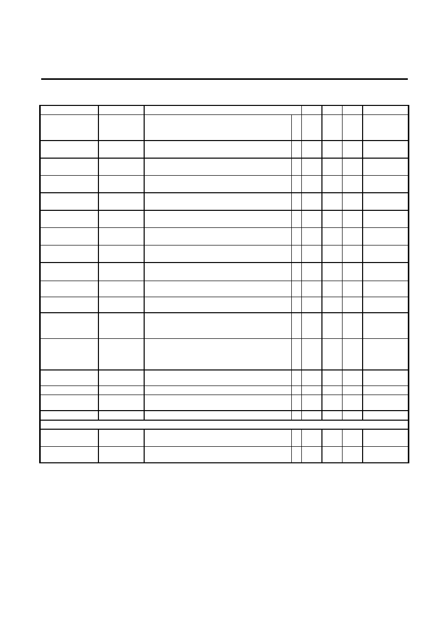
Electrical Characteristics
(Note 1)
Electrical Characteristics at ILOAD = 0mA and TJ = +25
∞C unless otherwise specified.
Parameter Device
Test
Conditions
Min
Typ
Max
Units
Reference Voltage MIK5201
V
CONTROL
= 2.75V, V
POWER
= 2V, I
LOAD
= 10mA
V
CONTROL
= 2.7V to 12V,
V
POWER
= 3.3V to 5.5V, I
LOAD
= 10mA to 1A
*
1.238
1.230
1.250
1.250
1.262
1.270
V
Output Voltage
MIK5201-1.5
V
CONTROL
= 4V, V
POWER
= 2V
V
CONTROL
= 3V, V
POWER
= 2.3V, I
LOAD
= 0mA to 1A
*
1.485
1.475
1.500
1.500
1.515
1.525
V
MIK5201-2.5
V
CONTROL
= 5V, V
POWER
= 3.3V
V
CONTROL
= 4V, V
POWER
= 3.3V, I
LOAD
= 0mA to 1A
*
2.475
2.460
2.500
2.500
2.525
2.540
V
MIK5201-2.85
V
CONTROL
= 5.35V, V
POWER
= 3.35V
V
CONTROL
= 4.4V, V
POWER
= 3.7V, I
LOAD
= 0mA to 1A
*
2.821
2.805
2.850
2.850
2.879
2.895
V
MIK5201-3.0
V
CONTROL
= 5.5V, V
POWER
= 3.5V
V
CONTROL
= 4.5V, V
POWER
= 3.8V, I
LOAD
= 0mA to 1A
*
2.970
2.950
3.000
3.000
3.030
3.050
V
MIK5201-3.3
V
CONTROL
= 5.8V, V
POWER
= 3.8V
V
CONTROL
= 4.8V, V
POWER
= 4.1V, I
LOAD
= 0mA to 1A
*
3.267
3.247
3.300
3.300
3.333
3.353
V
MIK5201-3.5
V
CONTROL
= 6V, V
POWER
= 4V
V
CONTROL
= 5V, V
POWER
= 4.3V, I
LOAD
= 0mA to 1A
*
3.465
3.445
3.500
3.500
3.535
3.555
V
MIK5201-5.0
V
CONTROL
= 7.5V, V
POWER
= 5.5V
V
CONTROL
= 6.5V, V
POWER
= 5.8V, I
LOAD
= 0mA to 1A
*
4.950
4.920
5.000
5.000
5.050
5.080
V
Line Regulation
All
I
LOAD
= 10mA, (1.5V+ V
OUT
)
V
CONTROL
12V,
0.8V
(V
POWER
- V
OUT
)
5.5V
*
0.04
0.20
%
Load Regulation
All
V
CONTROL
= V
OUT
+2.5V, V
POWER
= V
OUT
+ 0.8V,
I
LOAD
= 10mA to 1A
* 0.08
0.40
%
Minimum Load
Current (Note 2)
MIK5201 V
CONTROL
= 5V, V
POWER
= 3.3V, V
ADJ
= 0V
*
1.7
5
mA
Control Pin Current
(Note3)
All V
CONTROL
= V
OUT
+2.5V, V
POWER
= V
OUT
+ 0.8V,
I
LOAD
= 10mA to 1A
*
20
mA
Ground Pin Current MIK5201-1.5/
-2.5/-2.85/
-3.0/-3.3/-3.5/-
5.0
V
CONTROL
= V
OUT
+2.5V, V
POWER
= V
OUT
+ 0.8V,
I
LOAD
= 10mA to 1A
* 5 10
mA
Adjust Pin Current MIK5201
V
CONTROL
= 2.75V, V
POWER
= 2.05V,
I
LOAD
= 10mA
* 50 120
µA
Current Limit
All
(V
IN
- V
OUT
) = 3V
* 1000 1500
mA
Ripple Rejection
All
V
CONTROL
= V
POWER
= V
OUT
+ 2.5V, V
RIPPLE
= 1V
P-P
,
I
LOAD
= 500mA
60 75
dB
Thermal Regulation MIK5201
T
A
= 25
∞C, 30 ms pulse
0.003
%/W
Dropout Voltage Note 4
Control Input
(V
CONTROL
- V
OUT
)
All V
POWER
= V
OUT
+0.8V, I
LOAD
= 10mA
V
POWER
= V
OUT
+ 0.8V, I
LOAD
= 1A
*
*
1.00
1.15
1.15
1.30
V
Power Input
(V
POWER
- V
OUT
)
All V
CONTROL
= V
OUT
+ 2.5V, I
LOAD
= 1A
*
0.55
0.70
V
The * denotes the specifications which apply over the full temperature range.
Note 1: Unless otherwise specified Vout = Vsense. For MIK5201 (adj) Vadj = 0V
Note 2: For the adjustable device the minimum load current is the minimum current required to maintain regulation. Normally the current
in the resistor divider used to set the output voltage is selected to meet the minimum load current requirement.
Note 3: The control pin current is the drive current required for the output transistor. This current will track output current with a ratio of
about 1:100.
Note 4: The dropout voltage for the MIK5201 is caused by either minimum control voltage or minimum power voltage.
The specifications represent the minimum input/output voltage required to maintain 1% regulation.
Page 2 of 6
Replacement of
CS5201-XX
MIK5201-XX
1 A Low Dropout Positive
Voltage Regulator
May 2000 - revised August 2000
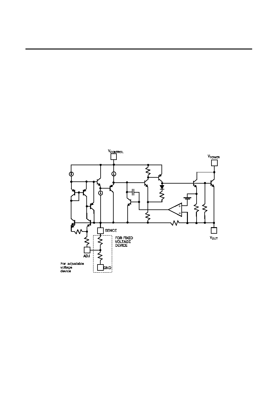
Pin Functions (5-Lead)
Sense (Pin 1): This pin is the positive side of the reference
voltage. With this pin it is possible to Kelvin sense the output
voltage at the load.
Adjust (Pin 2): This pin is the negative side of the reference
voltage. Adding a small bypass capacitor from the Adjust pin to
ground improves the transient response. For fixed voltage
devices the Adjust pin is also brought out to allow the user to
add a bypass capacitor.
GND (Pin 2): For fixed voltage devices this is the bottom of the
resistor divider that sets the output voltage.
V
POWER
(Pin 5): This pin is the collector of the power transistor.
The output load current is supplied through this pin. The
voltage at this pin must be 0.7V greater than the output voltage
for the device to regulate.
V
CONTROL
(Pin 4): This pin is the supply pin for the control
circuitry. The current flow into this pin will be about 1% of the
output current. The voltage at this pin must be 1.3V greater
than the output voltage for the device to regulate.
Output (Pin 3): This is the power output of the device.
Block Diagram
Page 3 of 6

Replacement of
CS5201-XX
MIK5201-XX
1 A Low Dropout Positive
Voltage Regulator
May 2000 - revised August 2000
Application Information
The MIK5201 is designed to make use of multiple
power supplies, to reduce the dropout voltage. One of the
advantages of the two supply approach is maximizing the
efficiency.
The second supply is at least 1V greater than output
voltage and is providing the power for the control circuitry and
supplies the drive current to the NPN output transistor. This
allows the NPN output transistor to be driven into saturation.
For the control voltage the current requirement is small equal
to about 1% of the output current. This drive current becomes
part of the output current. The maximum voltage on the Control
pin is 12V. The maximum voltage at the Power pin is 7V. By
tying the control and power inputs together the MIK5201 can
also be operated as a single supply device. In single supply
operation the dropout will be determined by the minimum
control voltage.
Both the fixed and adjustable versions have remote
sense pins, permitting very accurate regulation of output
voltage. As a result, over an output current range of 100mA to
1A, the typical load regulation is less than 1mV. For the fixed
voltages the adjust pin is brought out allowing the user to
improve transient response by bypassing the internal resistor
divider. Optimum transient response is provided using a
capacitor in the range of 0.1
µF to 1µF for bypassing the Adjust
pin.
In addition to the enhancements mentioned, the
reference accuracy has been improved a factor of two with a
guaranteed initial tolerance of
±1% at 25
0
C and 1.6% accuracy
over the full temperature and load current range.
Typical applications for the MIK5201 include 3.3V to
2.5V conversion with a 5V control supply, 5V to 4.2V
conversion with a 12V control supply or 5V to 3.6V conversion
with a 12V control supply. The device is fully protected against
overcurrent and overtemperature conditions.
Grounding and Output Sensing
The MIK5201 allows true Kelvin sensing for both the
high and low side of the load. As a result the voltage regulation
at the load can be easily optimized. Voltage drops due to
parasitic resistances between the regulator and the load can
be placed inside the regulation loop. The advantages of
remote sensing are illustrated in figures 1 through 3.
Figure 1 shows the device connected as a
conventional 3 terminal regulator with the Sense lead
connected directly to the output of the device. R
P
is the
parasitic resistance of the connections between the device and
the load. Trace A of figure 3 illustrates the effect of Rp.
Figure 2 shows the device connected to take
advantage of the remote sense feature. The Sense pin and the
top of the resistor divider are connected to the top of the load;
the bottom of the resistor divider is connected to the bottom of
the load. The effect on output regulation can be seen in trace
B of figure 3.
It is important to note that the voltage drops due to
R
P
are not eliminated; they will add to the dropout voltage of
the regulator regardless. The MIK5201 can control the voltage
at the load as long as the input-output voltage is greater than
the total of the dropout voltage of the device plus the voltage
drop across R
P
.
POWER
SENSE
OUTPUT
ADJ
R
P
R
P
CONTROL
MIK5201
3.3V
5.0V
LOAD
R2
R1
Figure 1. Conventional Load Sensing
POWER
SENSE
OUTPUT
ADJ
R
P
R1
R2
R
P
CONTROL
MIK5201
3.3V
5.0V
LOAD
Figure 2. Remote Load Sensing
V
OUT
V
OUT
FIGURE 1
A
B
FIGURE 2
TIME
I
OUT
(I
)(R )
OUT
P
Figure 3. Remote Sensing Improves Load Regulation
Page 4 of 6
Replacement of
CS5201-XX
MIK5201-XX
1 A Low Dropout Positive
Voltage Regulator
May 2000 - revised August 2000
Stability
The circuit design used in the MIK5201 series
requires the use of an output capacitor as part of the device
frequency compensation. The addition of 150
µF aluminum
electrolytic or a 22
µF solid tantalum on the output will ensure
stability for all operating conditions.
Output Voltage
The MIK5201 (adjustable version) develops a 1.25V
reference voltage between the Sense pin and the Adjust pin
(Figure 4). Placing a resistor between these two terminals
causes a constant current to flow though R1 and down though
R2 to set the output voltage. In general R1 is chosen so that
this current is the specified minimum load current of 5 mA. The
current out of the Adjust pin is small, typically 50
µA and it adds
to the current from R1. For best regulation the top of the
resistor divider should be connected directly to the Sense pin.
Figure 4. Setting Output Voltage
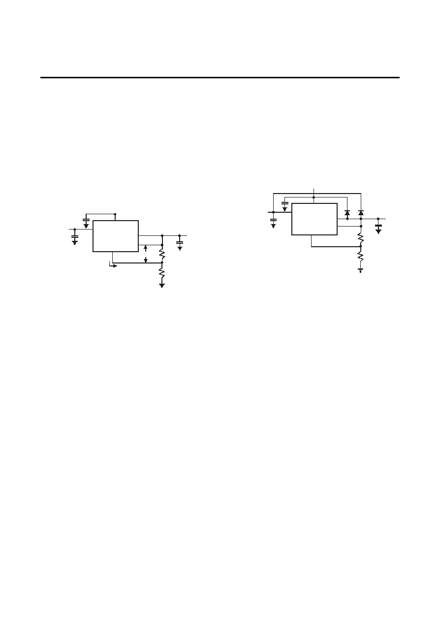
Protection Diodes
In normal operation MIK5201 family does not need
any protection diodes between the adjustment pin and the
output and from the output to the input to prevent die
overstress. Internal resistors are limiting the internal current
paths on the ADJ pin. Therefore even with bypass capacitors
on the adjust pin no protection diode is needed to ensure
device safety under short-circuit conditions. The Adjust pin can
be driver on a transient basis
±7V with respect to the output
without any device degradation.
A protection diode between the Output pin and
V
POWER
pin is not usually needed. Microsecond surge currents
of 50A to 100A can be handled by the internal diode between
the Output pin and V
POWER
pin of the device. In normal
operations it is difficult to get those values of surge currents
even with the use of large output capacitances. Only with high
value output capacitors, such as 1000
µF to 5000µF and the
V
POWER
pin is instantaneously shorted to ground, damage can
occur. A diode from output to input is recommended (Figure 5).
If MIK5201 is connected as a single supply device
with the control and power input pins shorted together the
internal diode between the output and the power input pin will
protect the control input pin.
POWER
SENSE
OUTPUT
ADJ
D1
D2
R1
R2
V
OUT
V
POWER
V
CONTROL
CONTROL
MIK5201
+
+
+
POWER
SENSE
OUTPUT
ADJ
R1
R2
V
OUT
I
ADJ
50 A
µ
V
REF
V
OUT
=
I
R2
ADJ
V
(1+R2/R1) +
REF
V
POWER
V
CONTROL
CONTROL
MIK5201
+
+
+
Figure 5. Optional Clamp Diodes Protect Against Input
Crowbar Circuits
Thermal Considerations
The MIK5201 series have internal power and
thermal limiting circuitry designed to protect the device under
overload conditions. However maximum junction temperature
ratings should not be exceeded under continuous normal load
conditions. Careful consideration must be given to all sources
of thermal resistance from junction to ambient, including
junction-to-case, case-to-heat sink interface and heat sink
resistance itself.
Junction temperature of the Control section can run up to
125
0
C. Junction temperature of the Power section can run up
to 150
0
C.
Page 5 of 6
Replacement of
CS5201-XX
MIK5201-XX
1 A Low Dropout Positive
Voltage Regulator
May 2000 - revised August 2000
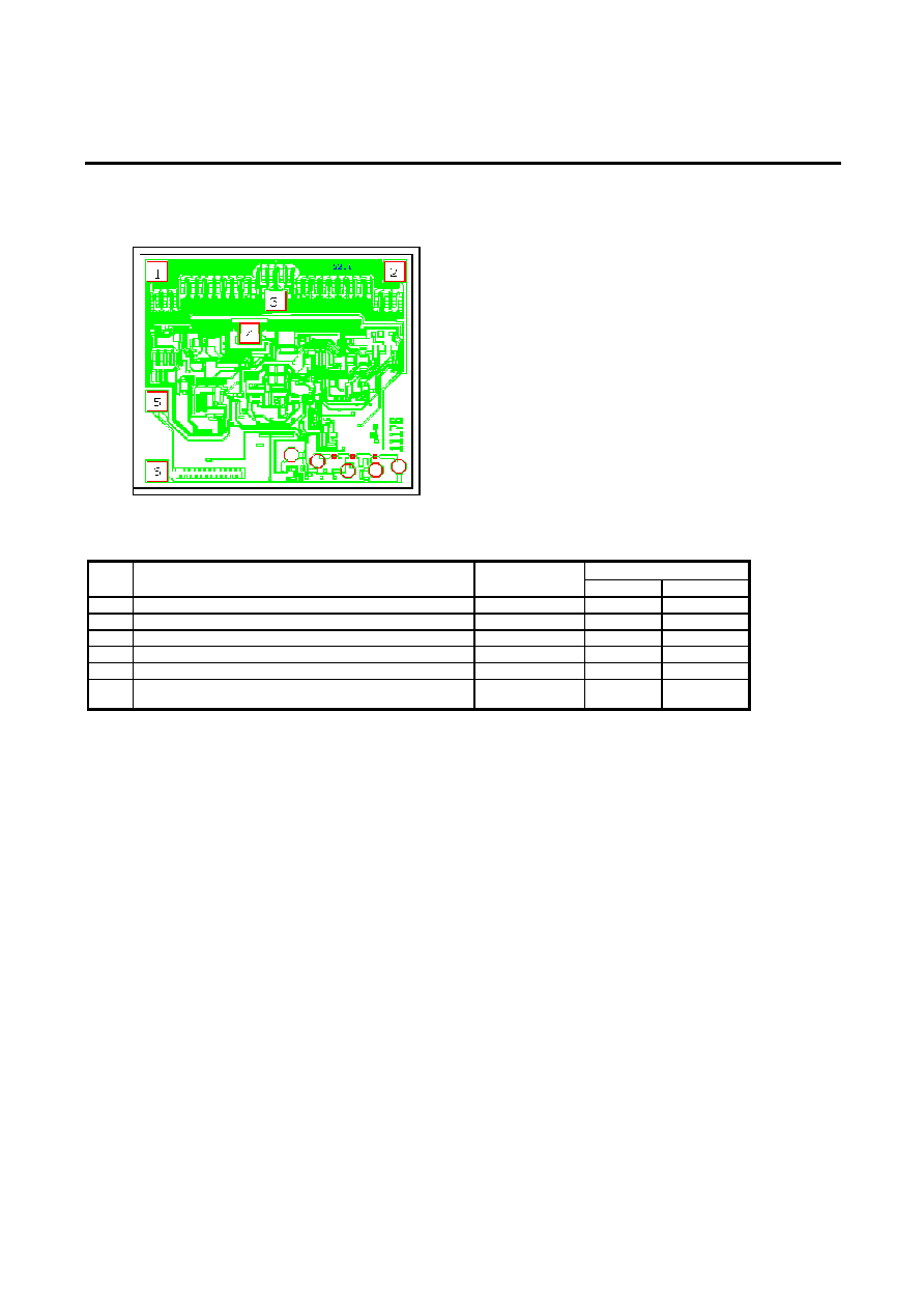
Pad Location MIK5201-XX
Chip size 2.0 mm x 1.78 mm
Pad Location Coordinates
Coordinates (
µm)
N Pad
Name
Pad size (
µm
◊ µm)
X Y
1 Output
140
◊ 140
170 1610
2 Output
140
◊ 140
1830 1610
3 V
POWER
(Note1)
140
◊ 140
1000 1397
4 V
CONTROL
(Note1)
140
◊ 140
816 1163
5
Sense (Note 1)
140
◊ 140
170 675
6
Adjust (adjustable output)
GND (fixed output)
140
◊ 140
170 170
Note 1: For 3-lead version connect 3, 4 pad to V
IN
and 5 pad to Output
Page 6 of 6