 | –≠–ª–µ–∫—Ç—Ä–æ–Ω–Ω—ã–π –∫–æ–º–ø–æ–Ω–µ–Ω—Ç: MIK 5203 | –°–∫–∞—á–∞—Ç—å:  PDF PDF  ZIP ZIP |
MI
KRON
JS
C
∑
ht
t
p
:
//ww
w
.mikron.ru
∑
19 A
u
gus
t
2003
MIK5203 series
∑
3A LOW DROPOUT POSITIVE VOLTAGE REGULATOR
1
DATA SHEET
19 August 2003
N
O
. 00014
R
EV
1-03
CONTENTS
Page
GENERAL DESCRIPTION
1
FEATURES
1
BLOCK DIAGRAM
2
PIN ASSIGNMENTS
2
TYPICAL APPLICATION CIRCUIT
2
FIXED VOLTAGE REGULATOR
2
ADJUSTABLE VOLTAGE REGULATOR
2
ABSOLUTE MAXIMUM RATINGS
2
ELECTRICAL CHARACTERISTICS
3
TYPICAL CHARACTERISTICS
4
DROPOUT VOLTAGE (V
IN
≠ V
OUT
)
4
MINIMUM OPERATING CURRENT (ADJUSTABLE
DEVICE)
4
SHORT-CIRCUIT CURRENT
4
LOAD REGULATION
4
RIPPLE REJECTION
4
RIPPLE REJECTION VERSUS CURRENT
4
TEMPERATURE STABILITY
5
ADJUST PIN CURRENT
5
TYPICAL APPLICATIONS
5
1.2V TO 5.5V ADJUSTABLE REGULATOR
5
5V REGULATOR WITH SHUTDOWN
5
CONTENTS
Page
BATTERY CHARGER
5
IMPROVING RIPPLE REJECTION
5
LOW DROPOUT NEGATIVE SUPPLY
5
AUTOMATIC LIGHT CONTROL
5
ACTIVE TERMINATOR FOR SCSI-2 BUS
5
BATTERY BACKED UP REGULATED SUPPLY
5
HIGH EFFICIENCY DUAL SUPPLY
6
HIGH EFFICIENCY REGULATOR
6
APPLICATION INFORMATION
7
STABILITY
7
PROTECTIONS DIODES
7
OUTPUT VOLTAGE
7
LOAD REGULATION
7
RIPPLE REJECTION
7
PHYSICAL DIMENSIONS AND MARKING
DIAGRAMS
9
TO-220-3
9
TO-263-3
9
ORDERING INFORMATION
10
GENERAL DESCRIPTION
The MIK5203 is a positive low dropout regulator
designed to provide up to 3A of output current. The
device is available in an adjustable version and fixed
output voltages of 1.8V, 2.5V, 3.0V and 3.3V. All
internal circuitry is designed to operate down to 1V
input to output differential. Dropout voltage is
guaranteed at a maximum of 1.3V at 3A, decreasing
at lower load currents. On chip trimming adjusts the
reference/output voltage to within ±1%.
The MIK5203 requires a minimum of 22µF of output
capacitance for stability. Output capacitors of this
size or larger are normally included in most regulator
designs.
Unlike PNP type regulators where up to 10% of the
output current is wasted as quiescent current, the
quiescent current of the MIK5203 flows into the load,
increasing efficiency.
FEATURES
∑
Adjustable or Fixed Output
∑
Output Current of 3A
∑
Low Dropout, 1.15V at 3A Output Current
∑
0.04% Line Regulation
∑
0.08% Load Regulation
∑
100% Thermal Limit Burn-In
∑
Fast Transient Response
REPLACEMENT
of
CS5203
MIK5203-xx series
3A LOW DROPOUT POSITIVE VOLTAGE REGULATOR
2
Design by Vladimir F.Lityaghin / E-mail: lityaghin@mail.ru / Tel: +7(095)532-64-54
MI
KRON
JS
C
∑
h
ttp:
/
/www.
mi
kr
o
n
.
r
u
∑
19 A
u
gu
st
2003
3A LOW DROPOUT POSITIVE VOLTAGE REGULATOR
∑
MIK5203 series
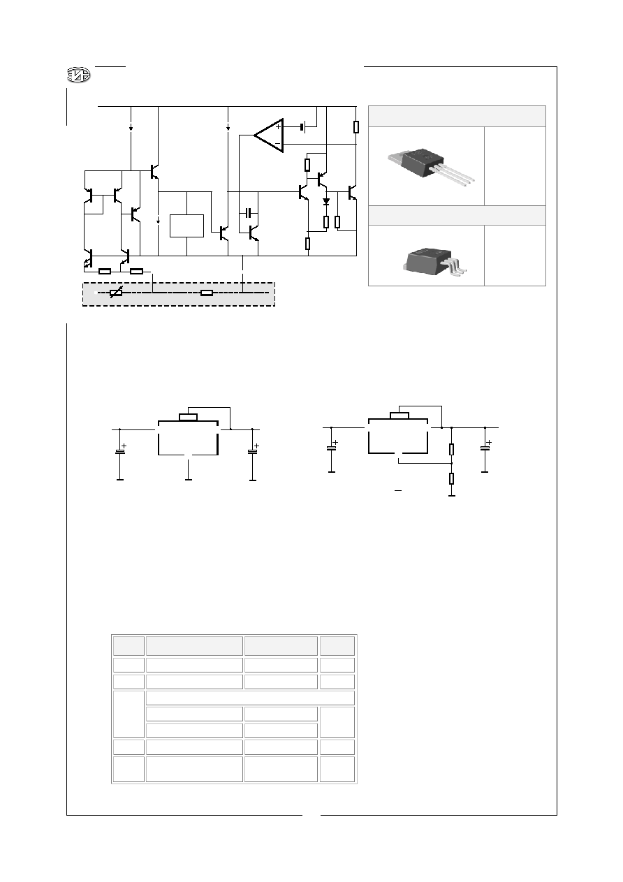
BLOCK DIAGRAM
!
!
!
GND
ADJ
OUT
IN
FOR FIXED VOLTAGE DEVICE
THERMAL
LIMIT
"
"
"
"
"
"
"
"
"
"
"
"
"
"
"
"
"
"
"
"
"
"
"
"
"
"
"
"
"
"
"
"
"
"
!
!
!
!
ABSOLUTE MAXIMUM RATINGS
TYPICAL APPLICATION CIRCUIT
FIXED VOLTAGE REGULATOR
NOTES:
∑
C1 needed if device is far from filter capacitors
∑
C2 minimum value required for stability
C1
C2
10µF
22µF
V
IN
> 4.75V
V
OUT
= 3.3V
V
IN
V
OUT
MIK5203-3.3
GND
TAB
!
2
!
3
!
1
!
!
!
!
!
PIN ASSIGNMENTS
MIK5203-xx
T
, MIK5203
T
TO-220-3
TAB
-- V
OUT
1 -- ADJ/GND
2 -- V
OUT
3 -- V
IN
MIK5203-xx
D2T
, MIK5203
D2T
TO-263-3
TAB
-- V
OUT
1 -- ADJ/GND
2 -- V
OUT
3 -- V
IN
TAB
2
1
3
TAB
TAB
C1
C2
R1
R2
232
1%
133
1%
10µF
22µF
V
IN
> 4.75V
V
OUT
= 3.45V
V
IN
V
OUT
MIK5203
ADJ
!
2
!
3
!
1
!
!
!
!
!
!
!
ADJUSTABLE VOLTAGE REGULATOR
(
)
2
1
1
2
R
I
V
V
ADJ
R
R
REF
OUT
◊
+
+
=
2
1
3
NOTE:
Stresses above those listed under ´Absolute
Maximum Ratingsª may cause permanent
damage to the device. These are stress
ratings only and functional operation of the
device at these or any other conditions
above those indicated in the operation
sections of the specifications is not implied.
Exposure to Absolute Maximum Rating
conditions for extended periods may affect
device reliability.
SYMBOL
PARAMETER
MAXIMUM
UNIT
P
D
Power Dissipation
Internally Limited
W
V
IN
Input Voltage
7
V
Operating Junction Temperature Range
Control Section
0 to 125
T
J
Power Transistor
0 to 150
∫C
T
STG
Storage Temperature
-65 to 150
∫C
T
LEAD
Lead Temperature
Soldering, 10sec)
300
∫C
MI
KRON
JS
C
∑
ht
t
p
:
//ww
w
.mikron.ru
∑
19 A
u
gus
t
2003
MIK5203 series
∑
3A LOW DROPOUT POSITIVE VOLTAGE REGULATOR
3
The # denotes the specifications which apply over the full temperature range.
Note 1: For MIK5203 (adjustable) Vadj = 0V
Note 2: For the adjustable device the minimum load current is the minimum current required to maintain
regulation. Normally the current in the resistor divider used to set the output voltage is selected to
meet the minimum load current requirement.
Note 3: The specification represent the minimum input/output voltage required to maintain 1% regulation.
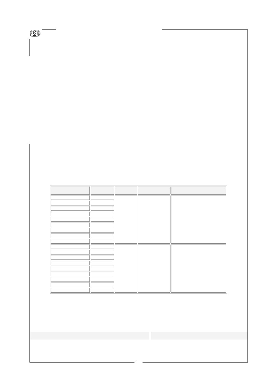
ELECTRICAL CHARACTERISTICS
Electrical Characteristics at I
LOAD
= 0 mA and T
J
= +25
∞
C unless otherwise specified.
PARAMETER
DEVICE
TEST CONDITIONS
MIN
TYP
MAX UNIT
V
IN
= 2.75V, I
LOAD
= 10mA
1.238 1.250 1.262
Reference Voltage
(Note 1)
MIK5203
V
IN
= 2.7V to 12V, I
LOAD
= 10mA to 3A
#
1.230 1.250 1.270
V
V
IN
= 4.0V
1.485
1.500 1.515
MIK5203-1.5
V
IN
= 3.0V, I
LOAD
= 0mA to 3A
#
1.475 1.500 1.525
V
V
IN
= 4.3V
1.782 1.800 1.818
MIK5203-1.8
V
IN
= 3.3V, I
LOAD
= 0mA to 3A
#
1.771 1.800 1.829
V
V
IN
= 5.0V
2.475 2.500 2.525
MIK5203-2.5
V
IN
= 4.0V, I
LOAD
= 0mA to 3A
#
2.460 2.500 2.540
V
V
IN
= 5.35V
2.821 2.850 2.879
MIK5203-2.85
V
IN
= 4.40V, I
LOAD
= 0mA to 3A
#
2.805 2.850 2.895
V
V
IN
= 5.5V
2.970 3.000 3.030
MIK5203-3.0
V
IN
= 4.5V, I
LOAD
= 0mA to 3A
#
2.950 3.000 3.050
V
V
IN
= 5.8V
3.267 3.300 3.333
MIK5203-3.3
V
IN
= 4.8V, I
LOAD
= 0mA to 3A
#
3.247 3.300 3.353
V
V
IN
= 6.0V
3.465 3.500 3.535
MIK5203-3.5
V
IN
= 5.0V, I
LOAD
= 0mA to 3A
#
3.445 3.500 3.555
V
V
IN
= 7.5V
4.950 5.000 5.050
Output Voltage
MIK5203-5.0
V
IN
= 6.5V, I
LOAD
= 0mA to 3A
#
4.920 5.000 5.080
V
L
INE
R
EGULATION
(Note 1)
All
I
LOAD
= 10mA, (1.5V+ V
OUT
) V
IN
12V #
0.04
0.2 %
L
OAD
R
EGULATION
(Note 1)
All
V
IN
= V
OUT
+2.5V, I
LOAD
= 10mA to 3A
#
0.08
0.4 %
M
INIMUM
L
OAD
C
URRENT
(Note 1, 2)
MIK5203
V
IN
= 5V
#
1.7
5.0
mA
G
ROUND
P
IN
C
URRENT
MIK5203-
1.5 /1.8/2.5/
2.85/3.0/3.3/
3.5 /5.0
V
IN
= V
OUT
+2.5V, I
LOAD
= 10mA to 3A
#
5 10
mA
A
DJUST
P
IN
C
URRENT
(Note 1)
MIK5203
V
IN
= 2.75V, I
LOAD
= 10mA
#
50
120
µA
C
URRENT
L
IMIT
(Note 1)
All (V
IN
- V
OUT
) = 3V
#
3 4 A
R
IPPLE
R
EJECTION
(Note 1)
All
V
IN
= V
OUT
+ 2.5V, I
LOAD
= 1.5A
60 75 dB
T
HERMAL
R
EGULATION
(Note 1)
MIK5203
T
A
= 25∞C, 30ms pulse
0.003
%/W
D
ROPOUT
V
OLTAGE
(Note 1, 3)
All
I
LOAD
= 10mA
I
LOAD
= 3A
#
1.00
1.15
1.15
1.30
V

4
Design by Vladimir F.Lityaghin / E-mail: lityaghin@mail.ru / Tel: +7(095)532-64-54
MI
KRON
JS
C
∑
h
ttp:
/
/www.
mi
kr
o
n
.
r
u
∑
19 A
u
gu
st
2003
3A LOW DROPOUT POSITIVE VOLTAGE REGULATOR
∑
MIK5203 series
TYPICAL CHARACTERISTICS
DROPOUT VOLTAGE (V
IN
≠ V
OUT
)
MINIMUM OPERATING CURRENT
(A
DJUSTABLE
D
EVICE
)
SHORT-CIRCUIT CURRENT
LOAD REGULATION
RIPPLE REJECTION
RIPPLE REJECTION versus CURRENT
1.5
1.0
0.5
2.5
3.0
3.5
4.0
1
2
3
4
5
6
7
0
SHO
R
T
CI
RC
U
I
T
CU
RRE
N
T
(A
)
INPUT OUTPUT DIFFERENTIAL
/
(V)
T
J
= 125∫C
T
J
= 25∫C
I
LOAD
= 3A
0.10
0.05
-0.05
-0.10
-0.15
-0.20
25
50
75
100
125
0
0
OU
T
P
U
T
V
O
L
T
AG
E
D
E
V
I
A
T
I
O
N
(%
)
TEMPERATURE (∫C)
V
RIPPLE
3V
P-P
V
RIPPLE
0.5V
P-P
(
-
)
V V
IN
OUT
3V
(
-
)
V V
IN
OUT
V
DROPOUT
C
f
ADJ
= 200µF at < 60Hz
C
f
I
ADJ
OUT
= 25µF at > 60Hz
= 1.5A
10
20
30
40
50
60
70
80
90
100
10
100
1k
10k
100k
0
R
I
PPLE
R
E
J
E
C
T
I
O
N
(d
B
)
FREQUENCY (Hz)
V
RIPPLE
3V
P-P
f
RIPPLE
= 120Hz
f
RIPPLE
= 20kHz
V
RIPPLE
0.5V
P-P
V = 5V
= 25µF
OUT
OUT
C
C
ADJ
= 25µF
10
20
30
40
50
60
70
80
90
100
0.5
1.0
1.5
2.5
3.0
2.0
0
R
I
PPLE
R
E
J
E
C
T
I
O
N
(d
B
)
OUTPUT CURRENT (A)
T
J
= 125∫C
T
J
= 25∫C
T
J
= 0∫C
1
1
2
2
3
3
4
4
5
6
7
0
M
I
N
I
MU
M O
P
E
R
A
T
I
N
G
C
U
RRE
N
T
(m
A
)
INPUT OUTPUT DIFFERENTIAL
/
(V)
T
J
= 25∫C
T
J
= 125∫C
1.4
1.2
1.0
0.8
0.6
0.4
0.2
3.0
0.5
1.0
1.5
2.0
2.5
0
DR
O
P
O
U
T V
O
L
T
A
G
E
(V
)
OUTPUT CURRENT (A)

MI
KRON
JS
C
∑
ht
t
p
:
//ww
w
.mikron.ru
∑
19 A
u
gus
t
2003
MIK5203 series
∑
3A LOW DROPOUT POSITIVE VOLTAGE REGULATOR
5
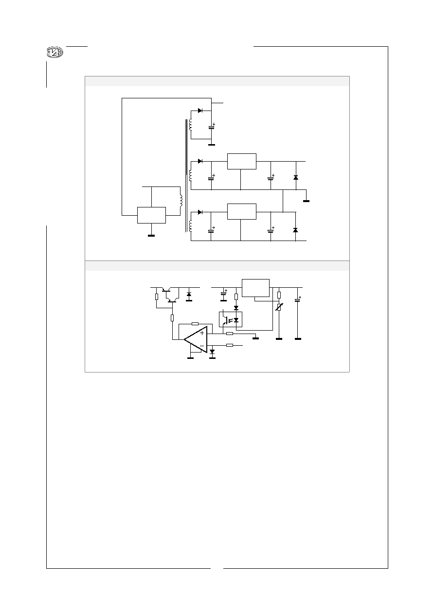
ACTIVE TERMINATOR FOR SCSI-2 BUS
BATTERY BACKED UP REGULATED SUPPLY
1.2V to 5.5V ADJUSTABLE
REGULATOR
5V REGULATOR WITH SHUTDOWN
BATTERY CHARGER
* N
EEDED
IF
DEVICE
IS
FAR
FROM
FILTER
CAPACITOR
** V
OUT
= 1.25 x (1 + (R2/R1))
IMPROVING RIPPLE REJECTION
LOW DROPOUT NEGATIVE SUPPLY
AUTOMATIC LIGHT CONTROL
*C1
IMPROVES
RIPPLE
REJECTION
. X
C
SHOULD
BE
R1
AT
RIPPLE
FREQUENCY
TYPICAL APPLICATIONS
TYPICAL CHARACTERISTICS
(CONTINUED)
TEMPERATURE STABILITY
ADJUST PIN CURRENT
10
20
30
40
50
60
70
80
90
100
25
50
75
100
125
0
A
D
J
U
ST
P
I
N
CURRE
N
T
(µ
A
)
TEMPERATURE (∫C)
-2.0
-1.0
1.0
2.0
0
25
50
75
100
125
0
O
U
TP
UT
V
O
L
T
A
G
E
CHA
N
G
E
(%
)
TEMPERATURE (∫C)
MIK5203
V
IN
**
V
OUT
C1
*
10µF
C2
100µF
R2
470
R1
121
IN
OUT
ADJ
∑
∑
∑
∑
∑
∑
MIK5203
V
IN
TTL
5V
100µF
121
1%
1k
1k
2N3904
10µF
366
1%
IN
OUT
ADJ
∑
∑
∑
∑
∑
∑
∑
∑
∑
∑
MIK5203
1.25V
IN
V
IN
V
OUT
R
S
R1
OUT
IF
ADJ
∑
∑
+
-
+
-
=
R1
R2
R
R1
R2
V
IF
S
OUT
1
1
1.25V
+
-
=
R1
R2
R
V
IF
S
OUT
1
1
MIK5203
IN
OUT
ADJ
V
IN
V
IN
16.5V
10µF
R2
350
1%
R1
121
1%
C1
10µF
150µF
∑
∑
∑
∑
∑
∑
∑
∑
V
IN
V
OUT
= -5V
FLOATING
INPUT
10µF
100µF
∑
∑
∑
∑
∑
∑
∑
∑
∑
MIK5203
IN
OUT
ADJ
MIK5203-
2.85
IN
OUT
GND
∑ ∑
18
t
o
27 l
i
n
e
s
4.75V
to
5.25V
110
110
110
110
22µF
10µF
∑
∑
∑
∑
∑
∑
∑
V
IN
5.2V
5.0V
LINE
BATTERY
SELECT FOR
CHARGE RATE
6.5V
50
10µF
10µF
100µF
MIK5203-
5.0
IN
OUT
GND
MIK5203-
5.0
IN
OUT
GND
∑
∑
∑
∑
∑
∑
MIK5203
10µF
100µF
1.2k
IN
OUT
ADJ
∑
∑
∑
∑
!
6
Design by Vladimir F.Lityaghin / E-mail: lityaghin@mail.ru / Tel: +7(095)532-64-54
MI
KRON
JS
C
∑
h
ttp:
/
/www.
mi
kr
o
n
.
r
u
∑
19 A
u
gu
st
2003
3A LOW DROPOUT POSITIVE VOLTAGE REGULATOR
∑
MIK5203 series
TYPICAL APPLICATIONS
(CONTINUED)
HIGH EFFICIENCY DUAL SUPPLY
HIGH EFFICIENCY REGULATOR
SWITCHING
REGULATOR
10µF
10µF
470µF
470µF
1N4002
1N4002
+5V
2A
- 5V
2A
+V
IN
3.3V OUTPUT (TYPICAL)
FEEDBACK PACK
MIK5203-
5.0
IN
OUT
GND
MIK5203-
5.0
IN
OUT
GND
∑
∑
∑
∑
∑
∑
∑
∑
∑
∑
∑
∑
∑
∑
∑
∑
∑
∑
∑
LT1011
!! !
!
MIK5203
IN
OUT
ADJ
100µF
1N914
1N914
4N28
NR1122
1k
470
240
2k
1M
10k
10k
10k
10 000µF
1mH
28V INPUT
28V
28V
OUTPUT
OUTPUT
ADJUST
∑
∑
∑
∑
∑
∑
∑
∑
∑
∑
∑
∑ ∑
∑
∑

MI
KRON
JS
C
∑
ht
t
p
:
//ww
w
.mikron.ru
∑
19 A
u
gus
t
2003
MIK5203 series
∑
3A LOW DROPOUT POSITIVE VOLTAGE REGULATOR
7
APPLICATION INFORMATION
The MIK5203 family of 3-terminal regulators are
easy to use. They are protected against short
circuit and thermal overloads. Thermal protection
circuitry will shut down the regulator should the
junction temperature exceed 170∞C at the sense
point. These regulators are pin compatible with
older 3-terminal adjustable regulators, offer lower
dropout voltage and more precise reference
tolerance. Reference stability over temperature is
improved over older types of regulators.
STABILITY
The MIK5203 family of regulators requires an
output capacitor as part of the device frequency
compensation. A minimum of 22mF of tantalum or
50mF of aluminum electrolytic is required. The ESR
of the output capacitor should be less than 0.5.
When using the MIK5203 adjustable device the
adjust terminal can be bypassed to improve ripple
rejection. When the adjust terminal is bypassed
the required value of the output capacitor
increases. The device will require an output
capacitor of 22mF tantalum or 150mF aluminum
electrolytic when the adjust pin is bypassed.
Normally, capacitor values on the order of 100mF
are used in the output of many regulators to ensure
good load transient response with large load
current changes. Output capacitance can be
increased without limit and larger values of output
capacitance further improve stability and transient
response.
PROTECTION DIODES
Diodes between input and output are not usually
needed. Only with extremely large output
capacitors, such
as 1000mF and
larger, and with
the input pin
instantaneously
s h o r t e d t o
g r o u n d c a n
damage occur. A
crowbar circuit
at the input of
the MIK5203 in
c o m b i n a t i o n
with a large
output capacitor could generate currents large
enough to cause damage. In this case a diode from
output to input is recommended, as shown in
Figure 1.
OUTPUT VOLTAGE
The MIK5203 develops a 1.25V reference voltage
between the output and the adjust terminal (see
Figure 2). By placing a resistor between these two
terminals, a constant current is caused to flow
through R1 and down through R2 to set the overall
ou tp ut v ol tag e.
Normally this current
is chosen to be the
specified minimum
load current of
10mA. Because IADJ
is very small and
c o n s t a n t w h e n
compared to the
current through R1,
it represents a small error and can usually be
ignored. For fixed voltage devices R1 and R2 are
included in the device.
LOAD REGULATION
Because the MIK5203 is a 3-terminal device, it is
not possible to provide true remote load sensing.
Load regulation will be limited by the resistance of
the wire connecting the regulator to the load. The
data sheet specification for load regulation is
measured at the output pin of the device. Negative
side sensing is a true Kelvin connection, with the
bottom of the output divider returned to the
negative side of the load. Although it may not be
immediately obvious, best load regulation is
obtained when the top of the resistor divider (R1)
is returned directly to the output pin of the device,
not to the load. This is illustrated in Figure 3.
Connected as
shown, RP is
not multiplied
by the divider
ratio. If R1
w
e
r
e
connected to
the load, the
e f f e c t i v e
r e s i s t a n c e
between the
regulator and
the load would
be:
For fixed voltage devices the top of R1 is internally
Kelvin connected, and the ground pin can be used
for negative side sensing.
RIPPLE REJECTION
The curves for Ripple Rejection were generated
using an adjustable device with the adjust pin
bypassed. These curves will hold true for all values
C
OUT
1000µF
,
R1
R1
R2
R
P
+
◊
R
P
=
Parasitic Line Resistance
IN
OUT
ADJ
MIK5203
V
IN
V
OUT
R1
FIGURE 1
R2
C
OUT
150µF
C
ADJ
10µF
D1
1N4002
(OPTIONAL)
∑
∑
∑
∑
∑
∑
IN
OUT
ADJ
MIK5203
V
IN
FIGURE 3.
CONNECTIONS FOR BEST LOAD REGULATION
CONNECT
R2 TO LOAD
CONNECT
R1 TO CASE
R
L
R
P
PARASITIC
LINE RESISTANCE
R1
R2
∑
IN
OUT
ADJ
MIK5203
V
IN
V
REF
FIGURE 3.
BASIC ADJUSTABLE REGULATOR
R1
R2
C
OUT
150µF
∑
∑
∑
(
)
2
1
1
2
R
I
V
V
ADJ
R
R
REF
OUT
◊
+
+
=
8
Design by Vladimir F.Lityaghin / E-mail: lityaghin@mail.ru / Tel: +7(095)532-64-54
MI
KRON
JS
C
∑
h
ttp:
/
/www.
mi
kr
o
n
.
r
u
∑
19 A
u
gu
st
2003
3A LOW DROPOUT POSITIVE VOLTAGE REGULATOR
∑
MIK5203 series
of output voltage. For proper bypassing, and ripple
rejection approaching the values shown, the
impedance of the adjust pin capacitor, at the
ripple frequency, should be < R1. R1 is normally in
the range of 100 to 200. The size of the
required adjust pin capacitor is a function of the
input ripple frequency. At 120Hz, with R1 = 100,
the adjust pin capacitor should be >13µF. At 10kHz
only 0.16µF is needed.
For fixed voltage devices, and adjustable devices
without an adjust pin capacitor, the output ripple
will increase as the ratio of the output voltage to
the reference voltage (V
OUT
/V
REF
). For example,
with the output voltage equal to 5V, the output
ripple will be increased by the ratio of 5V/1.25V. It
will increase by a factor of four. Ripple rejection
will be degraded by 12dB from the value shown on
the curve.

MI
KRON
JS
C
∑
ht
t
p
:
//ww
w
.mikron.ru
∑
19 A
u
gus
t
2003
MIK5203 series
∑
3A LOW DROPOUT POSITIVE VOLTAGE REGULATOR
9
PHYSICAL DIMENSIONS
AND
MARKING DIAGRAMS
TO-220-3
PACKAGE
TO-220-3
MARKING DIAGRAM
XX
-- output voltage
(see table below)
YY
-- Year
WW
-- Work Week
n
-- assembly location
TO-263-3
PACKAGE
TO-263-3
MARKING DIAGRAM
MIK
5203-
XX
YYWW/n
A
B
C
D
E
F
G
H
J K L M N
MILLIMETERS
INCHES
DIM
MIN
MAX
MIN
MAX
A
1.143 1.397 0.045 0.055
B
9.804 10.236 0.386 0.403
C
11.074 11.506 0.406 0.418
D
9.042 9.347 0.356 0.368
E
0.660 0.914 0.026 0.036
F
4.318 4.572 0.170 0.180
G
0.000 0.254 0.000 0.010
H
2.540 BSC
0.100 BSC
J
1.295 REF
0.051 REF
K
13.691 14.707 0.539 0.579
L
0.457 0.660 0.018 0.026
M
5∫ REF
5∫ REF
N
2.235 2.591 0.088 0.102
MILLIMETERS
INCHES
DIM
MIN
MAX
MIN
MAX
A
3.75
3.85 0.147 0.151
B
15.24
15.75 0.600 0.620
C
12.47
12.9 0.491 0.508
D
9.05
9.15 0.356 0.360
E
13.00
14.00 0.511 0.551
F
1.14
1.70 0.044 0.067
G
2.40
2.72 0.094 0.107
H
2.40
2.70 0.094 0.106
J
4.40
4.60 0.173 0.181
K
0.61
0.88 0.024 0.034
L
3.50
3.93 0.137 0.154
M
0.49
0.70 0.019 0.027
N
1.23
1.32 0.048 0.051
H
J K L M N
A
B
C
D
E
F
G
XX
-- output voltage
(see table below)
Y
-- Year
WW
-- Work Week
n
-- assembly location
XX
OUTPUT
VOLTAGE
Blank
Adjustable
15
1.5 V
33
3.3 V
35
3.5 V
5
5.0 V
18
1.8 V
25
2.5 V
28
2.85 V
3
3.0 V
XX
OUTPUT
VOLTAGE
Blank
Adjustable
15
1.5 V
33
3.3 V
35
3.5 V
5
5.0 V
18
1.8 V
25
2.5 V
28
2.85 V
3
3.0 V
MIK
5203-
XX
YYWW/n
10
Design by Vladimir F.Lityaghin / E-mail: lityaghin@mail.ru / Tel: +7(095)532-64-54
MI
KRON
JS
C
∑
h
ttp:
/
/www.
mi
kr
o
n
.
r
u
∑
19 A
u
gu
st
2003
3A LOW DROPOUT POSITIVE VOLTAGE REGULATOR
∑
MIK5203 series
ORDERING INFORMATION
NOTE: The form of packing is stipulated in the contract.
!
Address: 1
ST
Zapadny Proezd 12, Building 1, Zelenograd, Moscow, Russia, 124460
"
Telephone: +7 (095) 535-23-43; 536-85-44
#
Fax: +7 (095) 530-92-01
$
Email: export@mikron.ru
#
Tel/Fax: +86-755-329-7574
%
Voice: +86-755-329-7573
$
Email: miksz@963.net
MIKRON JSC Head Office
MIKRON ShenZhen Office
ORDERING NUMBER
OUTPUT
VOLTAGE
PACKAGE
OPERATING
TEMPERATURE
SHIPPING
MIK 5203 T Adjustable
MIK 5203-1.5 T 1.5
V
MIK 5203-1.8 T 1.8
V
MIK 5203-2.5 T 2.5
V
MIK 5203-2.85 T 2.85
V
MIK 5203-3.0 T 3.0
V
MIK 5203-3.3 T 3.3
V
MIK 5203-3.5 T 3.5
V
MIK 5203-5.0 T 5.0
V
TO-220-3
0
∞
C to + 70
∞
C
50 units/Rail
MIK 5203 D2T Adjustable
MIK 5203-1.5 D2T 1.5
V
MIK 5203-1.8 D2T 1.8
V
MIK 5203-2.5 D2T 2.5
V
MIK 5203-2.85 D2T 2.85
V
MIK 5203-3.0 D2T 3.0
V
MIK 5203-3.3 D2T 3.3
V
MIK 5203-3.5 D2T 3.5
V
MIK 5203-5.0 D2T 5.0
V
TO-263-3
0
∞
C to + 70
∞
C
50 units/Rail
&
800 units/Reel
The information presented in this Data sheet is believed to be accurate and
reliable. Application circuits shown are typical examples illustrating the
operation of the device.
In the interest of product improvement, MIKRON reserves the right to change
specifications and data without notice and can assume no responsibility for
the use of any information, devices and application circuits described herein.
Reference to products of other manufacturers are solely for convenience and
do not imply total equivalency of design, performance, or otherwise.