MIK7023K-XX
32 KHz Standard
Watch Circuit
January 2002
Features
∑ Single 1.5 V battery operation
∑ High precision 32.768 KHz crystal controlled oscillator
∑ 1.3 V to 1.8 V operating voltage range
∑ 200 nA typical current consuption
∑ On-chip voltage regulator
∑ Integrated capacitors, mask-selectable
∑ Mask option for:
∑ pad designation
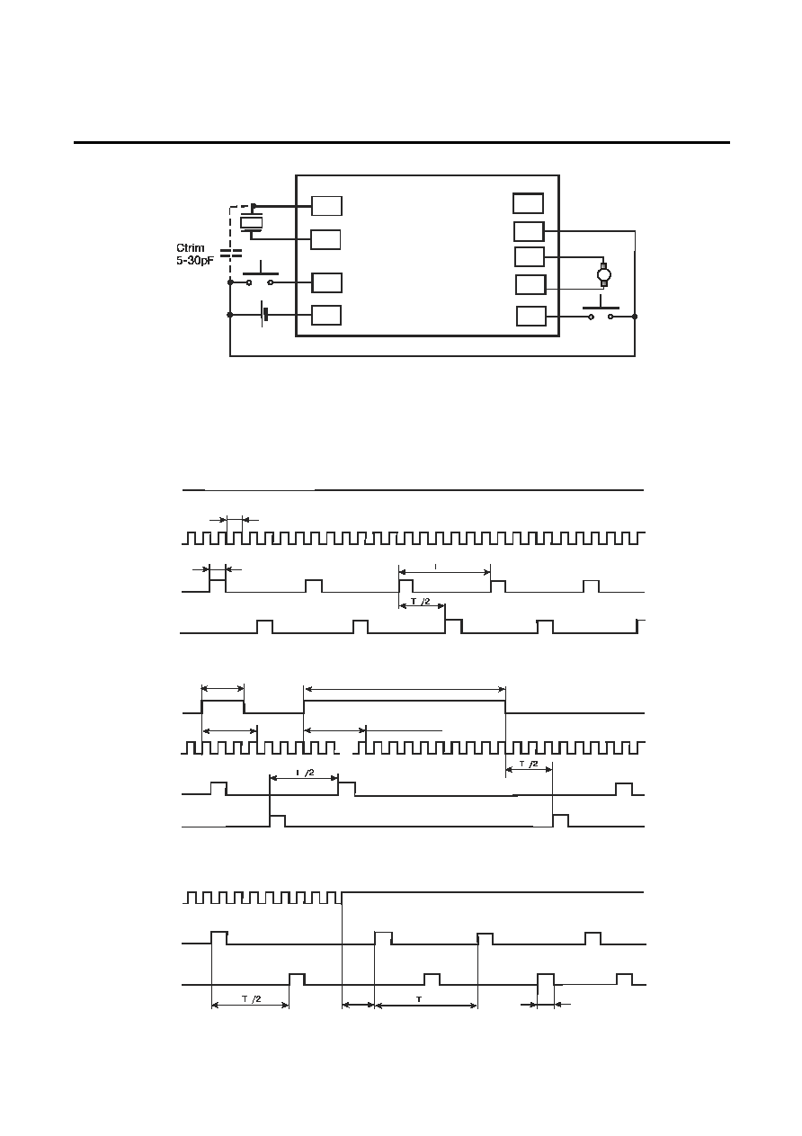
∑ motor period T
M
= 2, 4 ,6, 8, 10, 12, 20, 24, 30, 40, 60, or 120 sec
∑ motor pulse width t
M
= 0.98 to 14.65 in increments of 0.98 msec
∑ motor test cycle time T
MT
= 250, 125 or 62.5 msec
∑ Low resistance outputs for bipolar stepping motor
∑ Motor fast test function
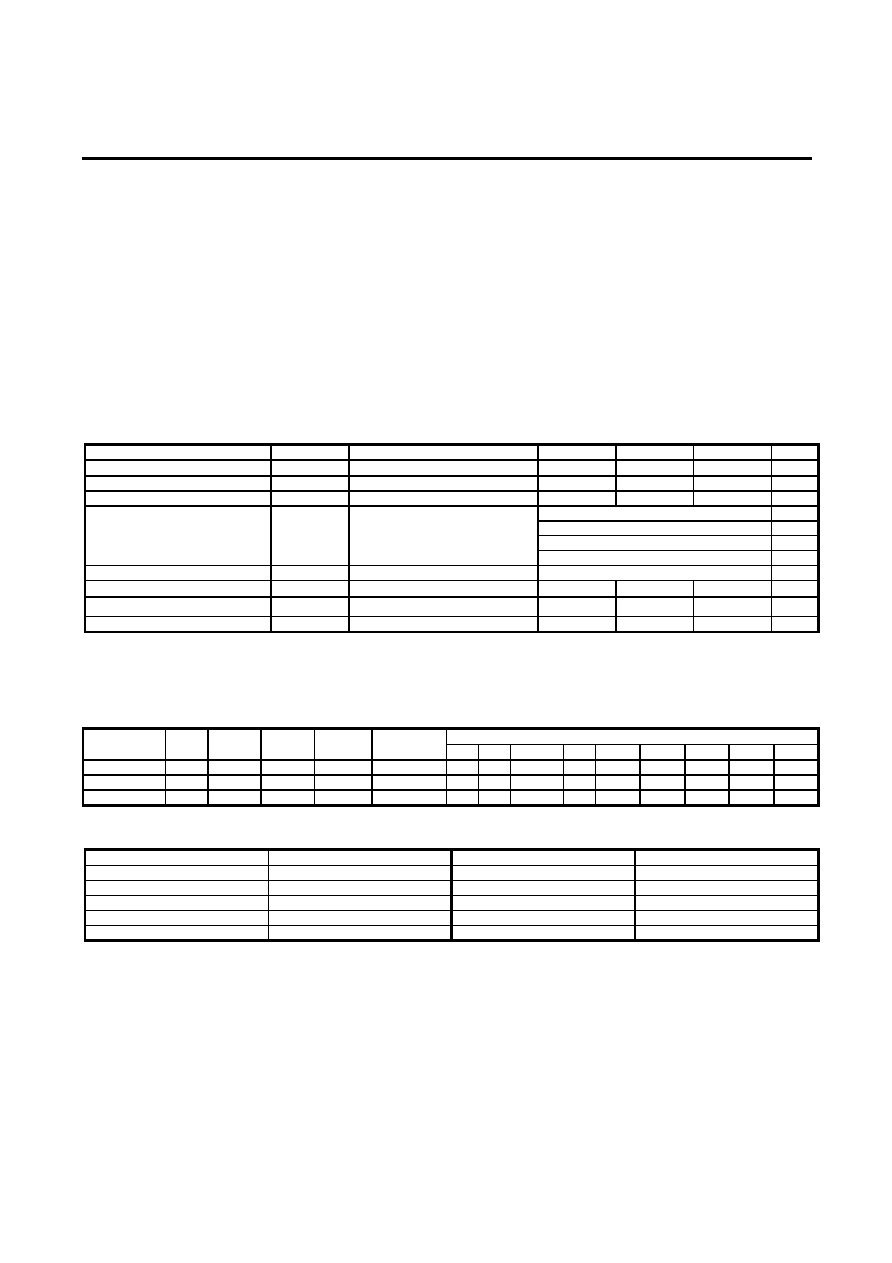
Electrical Characteristics
(V
DD
= 0 V, V
SS
= -1.5 V; T
a
= 25
o
C unless otherwise specified)
Parameters Symbol
Test
conditions Min
Typ
Max
Units
Operating Voltage
V
SS
1.3 1.5 1.8
V
Operating Current
I
DD
Without
Load
200
350
nA
Reset Input Current
I
IHR
V
IH
= 0 V
8
nA
See Option List
sec
See Option List
msec
Motor Outputs:
-Motor Cycle Time
-Motor Pulse Width
-Motor Test Cycle
T
M
t
M
T
MT
See Option List
msec
Time
Motor Outputs Current
I
M
R
L
= 2K, V
SS
= -1.55 V
0.7
mA
Oscillation Stability
F/F
V
SS
= -1.3V ~ -1.8V
1.0
ppm
Oscillator Start-up Voltage
V
ST
Within 2 sec
-1.3
V
* Quarts Crystal Parameters:
Frequency Fp =32768 Hz, Load capacitance C
L
= 12.5 pF
Static capacitance C
0
= 1.2 pF, Dynamic capacitance C
1
= 3.0 fF,
Series resistance R
S
= 35 K
Option List
Pad Designation
Number
IC
T
M,
sec
T
M,
msec
T
MT,
msec
COSCIN,
pF
COSCOUT,
pF
OI OO RESET
V
SS
TEST MOT2 MOT1 V
DD
V
GG
MIK7023K-01
2 5.86 125 16
16 1
2 3 4 5 6 7 8 9
MIK7023K-02
2 5.86 125 2
14 1
2 3 4 5 6 7 8 9
MIK7023K
-03
2 5.86 125 2
14 3
4 8 1 2 6 7 5 9
Pin Description (for MIK7023K-XX)
Pad Name
Description
Pad Name
Description
OI
Oscillator Input
MOT2
Motor Drive Output 2
OO
Oscillator Output
MOT1
Motor Drive Output 1
RESET Reset
Input
V
DD
Positive Power Supply
V
SS
Negative Power Supply
V
GG
Test Internal Voltage
TEST Test
Input/Output
Page 1 of 3