MIK7060K-XX
Circuit for Low Resistance Output Drivers
for Bipolar or Unpolar
Clock Stepping Motors
June 2001
Description
The MIK7060K-XX is low power integrated circuit in CMOS Silicon Gate technology designed to drive bipolar or unipolar clock stepping
motors. This device contains four identical and independent non-inverting circuits (MIK7060K-01) which can be connected by metal
mask programmation so as to obtain two identical non-inverting circuits with a lower resistance output (MIK7060K-02). Each buffer is
driven by a special cell which dephases the P and N transistor signal input for minimization of the transversal transition current. A tri-
state input HIZ with internal pull-down resistor provides the high impedance state of the four outputs.
Features
∑
Four low resistance output drivers for bipolar or unipolar
clock stepping motors
∑
Low transversal transition current
∑
Very low current consumption: 0.1 mA at 25
∞ C
∑
Two different output resistances programmable by metal
mask
∑
Wide power supply voltage range: 1.1 V to 3.5 V
∑
Tri-state input for applications as fast bus driver
∑
ESD and latch-up protections on input and output pads
Application
∑
Motor driver
∑
Bus driver
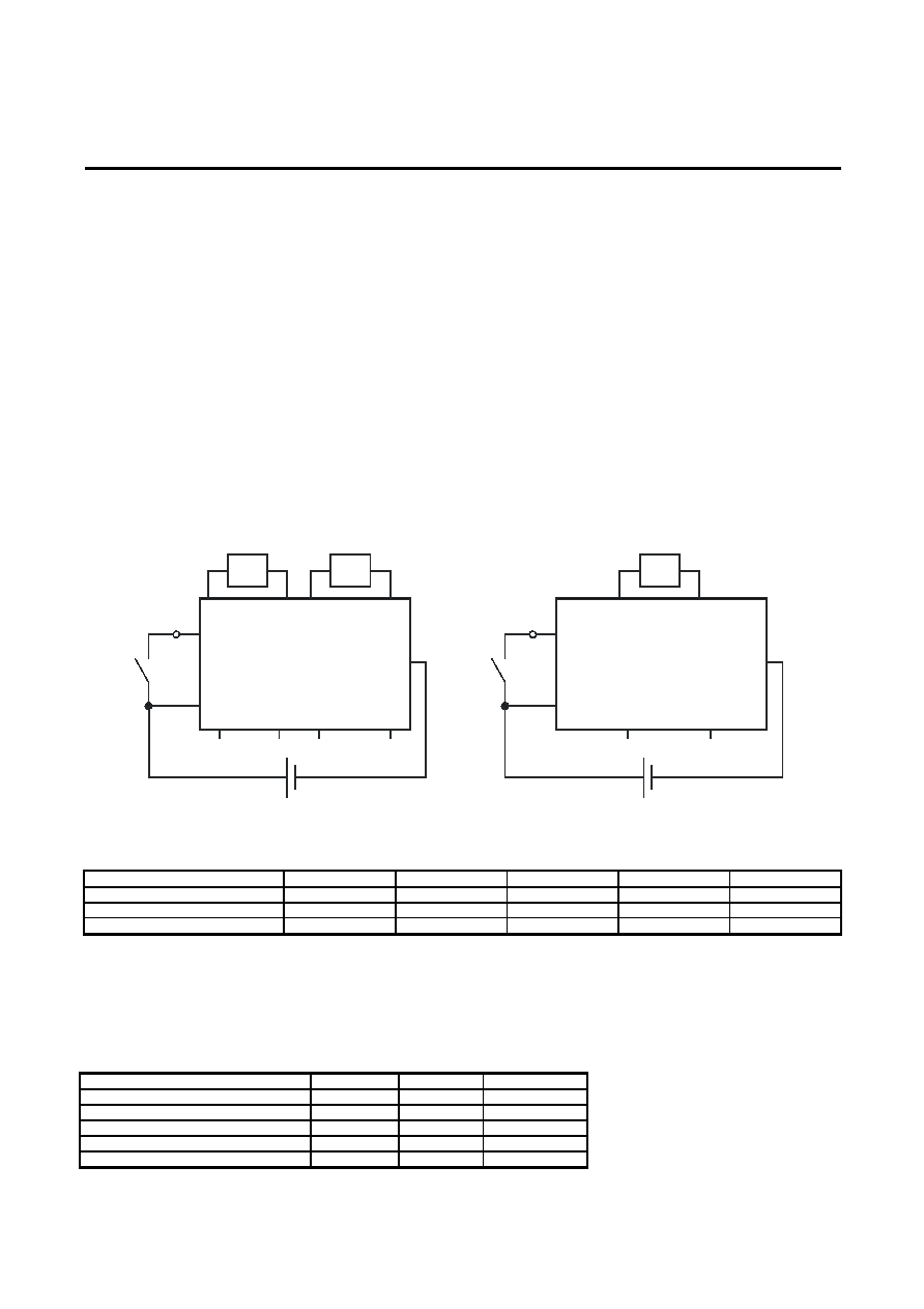
Function Diagram
+
M
M
OUT1
OUT2
OUT3
OUT4
IN1
IN2
IN3
IN4
HIZ
VDD
VSS
Rch = 200 Ohm
Rch = 200 Ohm
IN1
+
IN2
OUT2
OUT1
VSS
Rch = 200 Ohm
M
Figure 1.
HIZ
VDD
MIK7060K-01
MIK7060K-02
Absolute Maximum Ratings
Parameter Symbol
Min
Typ
Max
Units
Supply Voltage
VDD
-3.0 -- +5.5 V
Voltage at remaining pin
V
PIN
Vss-0.3 -- VDD+0.3 V
Storage Temperature
T
st
-55 -- +120 ∫C
Stresses beyond these listed maximum ratings may cause permanent damage to the device. Exposure to conditions beyond specified
operating conditions may affect device reliability or cause malfunction.
Handing Procedures
This device contains circuitry to protect the terminals against damage due to high static voltages or electrical fields. However, it is
advised that normal precautions be taken to avoid application of any voltage higher maximum rated voltages to this circuit.
Recommended Operating Conditions
Parameter Symbol
Value
Units
Ambient Temperature
T
25
∫C
Motor resistance
Rch
200
Ohm
Positive supply
VDD
1.55
V
Negative supply
VSS
0.0
V
Supply source resistance
Ri
10
Ohm
Page 1 of 3

MIK7060K-XX
Circuit for Low Resistance Output Drivers
for Bipolar or Unpolar
Clock Stepping Motors
June 2001
Electrical and Switching Characteristics
(at recommended operating conditions unless otherwise specified)
Parameter Symbol
Test
Condition
Min Typ Max
Units
Supply Voltage
VDD
1.1
1.5
3.5
V
Standby current
Isb
Outputs is open
IN1-IN4 at VDD or VSS, HIZ is open
-- -- 100
nA
Inputs:
VDD = 1.2 V
Pulse width
t
WL
ViL = VSS
1
--
--
mS
t
WN
ViH = VDD
1
--
--
mS
Voltage V
IL
Overal
Voltage
VSS
--
0.4 V
V
IH
Range
VDD-0.3 --
VDD V
HIZ input
current I
HIZ
HIZ at VDD = 1.55V
0.5
--
5
m A
Outputs:
Rch = 200 Ohm
Motor output
Iout
VDD = 1.2 V
current
MIK7060K-01
±4.3
-- --
mA
MIK7060K-02
±4.8
-- --
mA
VDD = 1.50 V
MIK7060K-01
±6.0
-- --
mA
MIK7060K-02
±6.4
-- --
mA
VDD = 3.0 V
MIK7060K-01
±13.0
-- --
mA
MIK7060K-02
±13.3
-- --
mA
Timing
Characteristic
Propogation
t
PHL
VDD = 1.2 V
--
--
100
ms
delay t
PLH
Cl = 30 pF
--
--
100
ms
Transition t
THL
--
--
100 ms
time t
TLH
--
--
100 ms
Operating
Temperature
Top
-20
--
+70
∫C
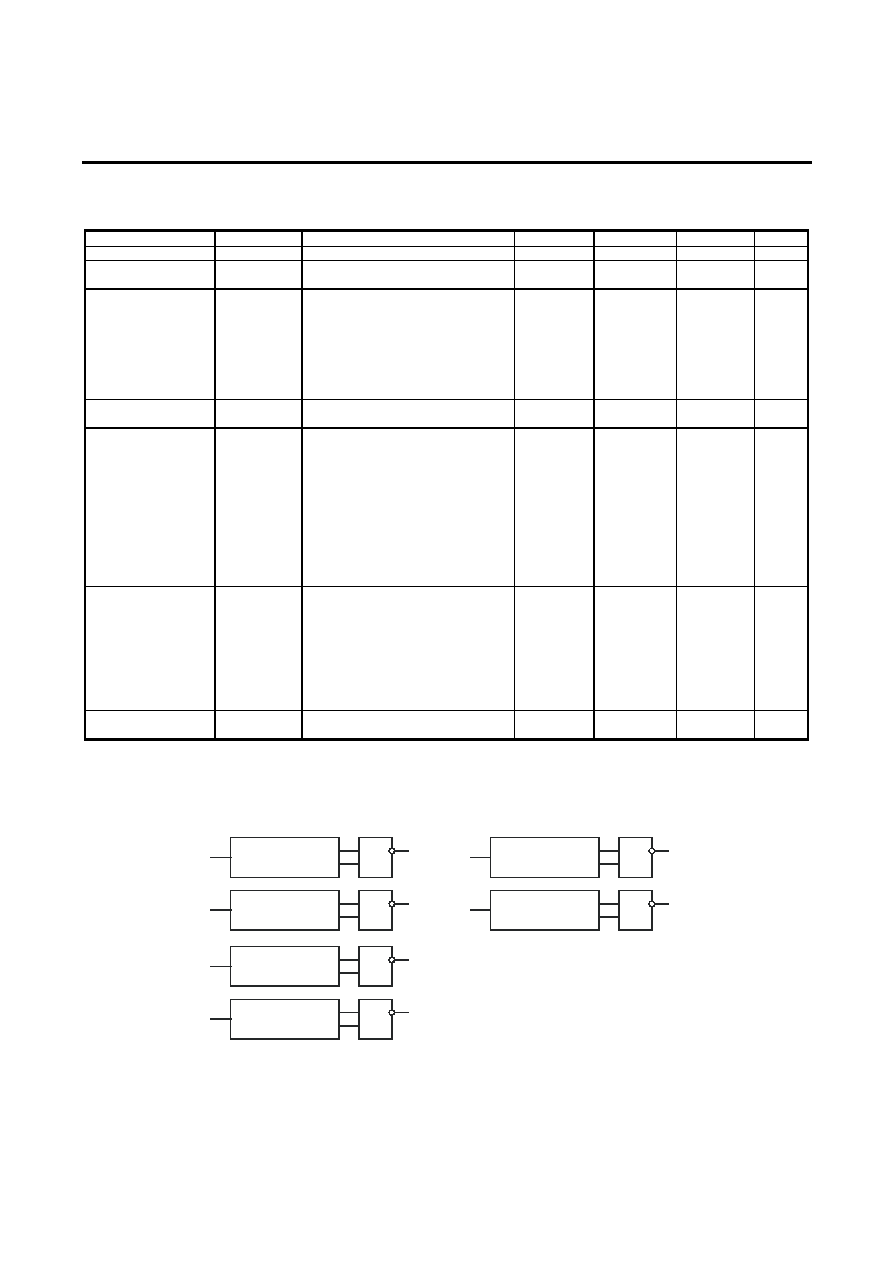
Block Diagram
Figure 2.
IN1
OUT1
Anti-current
Inverter
1
Anti-current
Inverter
IN2
1
OUT2
Anti-current
Inverter
IN3
1
OUT3
Anti-current
Inverter
IN4
1
OUT4
Anti-current
Inverter
Anti-current
Inverter
IN2
IN1
1
1
OUT2
OUT1
MIK7060K-01
MIK7060K-01
Page 2 of 3

MIK7060K-XX
Circuit for Low Resistance Output Drivers
for Bipolar or Unpolar
Clock Stepping Motors
June 2001
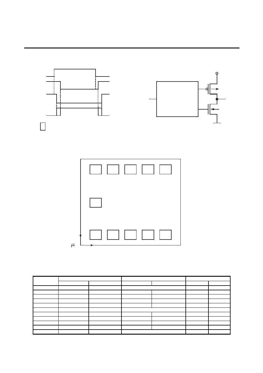
Timing Waveform
Figure 3.
IN
VGP
VGN
OUT
X
X
X : High impedance output
Function Description
Figure 4.
Anti-current
Inverter
IN
OUT
VDD
P
N
VGN
VGP
VSS
Pin Assignment
Chip Size: 1.3mm x 1.16mm
Pad Size: 100m x 100mm
2
3
4
5
6
10
11
9
8
7
VDD
OUT1
OUT2
OUT3
OUT4
(NC)
(OUT2)
(NC)
IN2
IN1
IN3
IN4
VSS
(IN1)
(NC)
(IN2)
(NC)
1
HIZ
MIK7060K-01/MIK7060K-02
Y
X
0 m
Substrate to VDD
(OUT1)
Pin Description
Pad Name
Function
Pad location
Pad number
7060K-01
7060K-02
7060K-01
7060K-02
X mm
Y mm
1
HIZ
HIZ
Tri-state input, pull-down
230
590
2
IN1
NC
Input 1
No contact
230
205
3
IN2
IN1
Input 2
Input 1
437
205
4
IN3
IN2
Input 3
Input 2
665
205
5
IN4
NC
Input 4
No contact
873
205
6
VSS
VSS
Negative Power Supply
1080
205
7
OUT4
NC
Output 4
No contact
1075
955
8
OUT3
OUT2
Output 3
Output 2
868
955
9
OUT2
OUT1
Output 2
Output 1
640
955
10
OUT1
NC
Output 1
No contact
432
955
11
VDD
VDD
Positive Power Supply
205
955
Page 3 of 3
