 | –≠–ª–µ–∫—Ç—Ä–æ–Ω–Ω—ã–π –∫–æ–º–ø–æ–Ω–µ–Ω—Ç: MIK 7088T | –°–∫–∞—á–∞—Ç—å:  PDF PDF  ZIP ZIP |

1
_
MIKA7088T
∑
FM RECEIVER CIRCUIT FOR BATTERY SUPPLY
MI
KRON
JS
C
∑
h
t
tp:
//w
ww.
mikr
o
n
.
r
u
∑
Dec
e
mber 2
2
,
SYMBOL PARAMETER
CONDITIONS
MIN
TYP
MAX
UNIT
V
P
Supply voltage
1.8 3.0 5.0 V
I
P
Supply current
4.2 5.2 6.6
mA
f
iRF
Radio input frequency
0.5 -- 110.0 MHz
V
i(rms)
RF sensitivity input voltage (RMS
value)
V
oAF
= -3dB;
V
oAF
=
0dB at V
i
= -1mV;
Mute OFF
-- 3
6.0
µ
V
Signal handling
f=±75 kHz; THD<10%
100 200 -- mV
V
o(rms)
Audio output signal (RMS value)
R
L
=22k
60 85 120
mV
T
amb
Operating ambient temperature
-10 --
+70
0
C
DATA SHEET
M
ARCH
2003
N
O
. 00007
R
EV
. 1-03
CONTENTS
Page
GENERAL DESCRIPTION
1
FEATURES
1
APPLICATIONS
1
QUICK REFERENCE DATA
1
PIN DESCRIPTION
AND
CONFIGURATION
2
BLOCK DIAGRAM
AND
APPLICATION
CIRCUIT FOR SEARCH TUNING
2
LIMITING VALUES
3
DC CHARACTERISTICS
3
CONTENTS
Page
AC CHARACTERISTICS
3
INPUT SENSITIVITY DIAGRAM
4
TEST
AND
APPLICATION INFORMATION
4
Test circuit and application for
mechanical tuning
4
Application circuit with AFC for
mechanical tuning
5
AM application circuit
5
PHYSICAL DIMENSIONS
AND
MARKING
DIAGRAM
6
ORDERING INFORMATION
6
SOP-16
6
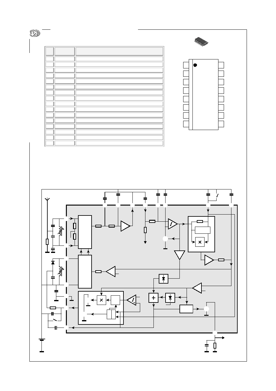
GENERAL DESCRIPTION
The MIKA7088T is a bipolar integrated circuit for
use in mono portable and pocket radios. It is used
when a minimum of peripheral components (of
small dimensions and low costs) is important. The
circuit contains a Frequency-Locked-Loop (FLL)
system with an Intermediate Frequency (IF) of
about 70 kHz. Selectivity is achieved by active RC-
filters. De-tuning related to the IF and too weak
input signals are suppressed by the mute circuit.
APPLICATIONS
∑
Mechanical tuning; this is possible with or
without integrating AFC circuit.
∑
Electrical tuning; this is realized by one
directional (band-up) search tuning facility,
including RESET to the lower-band limit.
FEATURES
∑
Equipped with all stages of a mono receiver from
antenna to audio output
∑
Mute circuit
∑
Search tuning with a single varicap diode
∑
Mechanical tuning with integrating AFC
∑
AM application supported
∑
Power supply polarity protection
∑
Power supply voltage down to 1.8 V
REPLACEMENT
of
TDA7088T
MIKA7088T
FM Receiver Circuit for Battery Supply
QUICK REFERENCE DATA

2
FM RECEIVER CIRCUIT FOR BATTERY SUPPLY
∑
MIKA7088T
Design by Vladimir F.Lityaghin / E-mail: lityaghin@mail.ru / Tel: +7(095)532-64-54
MI
KRON
JS
C
∑
h
t
tp:
//w
ww.
mikr
o
n
.
r
u
∑
Dec
e
mber 2
2
,
BLOCK DIAGRAM
&
APPLICATION CIRCUIT
FOR SEARCH TUNING
SOP-16
MIKA7088T
PIN DESCRIPTION
&
CONFIGURATION
PIN
SYMBOL
DESCRIPTION
1 MUTE
Mute output
2 V
oAF
Audio frequency output signal
3 LOOP
AF loop filter
4 V
P
+3 V supply voltage
5 OSC
Oscillator resonant circuit
6 IFFB
IF feedback
7 C
LP1
Low-pass capacitor of 1 db amplifier
8 V
oIF
IF output to external coupling capacitor (high-pass)
9 V
iIF
IF input to limiter amplifier
10 C
LP2
Low-pass capacitor of IF limiter amplifier
11 V
iRF
Radio frequency input
12 V
iRF
Radio frequency input
13 C
LIM
Limiter offset voltage capacitor
14 GND
Ground (0 V)
15 C
AP
All-pass filter capacitor / input for search tuning
16 TUNE
Electrical tuning / AFC output
1
2
3
4
5
6
7
8
16
15
14
13
12
11
10
9
MUTE
V
oAF
LOOP
V
P
OSC
IFFB
C
LP1
V
oIF
TUNE
C
AP
GND
C
LIM
V
iRF
V
iRF
C
LP2
V
iIF
Audio Frequency (
)
AF
AF
&
!
!
!
R
S
!
!
!
INTERMEDIATE
FREQUENCY
LIMITER
RUN
SEARCH TUNING
V2
V1
V1, V2, V3 are internal voltages.
V2
V3
V2
V
oAF
MUTE
-1
!
!
!
!
!
!
!
!
11
12
5
4
14
16
RESET
+3V
V
P
1
2
5.6k
82
pF
220pF
C16
68
pF
680
pF
0.1µF
0.1µF
10nF
22.0k
1.8nF
70
nH
L1
78
nH
BB910
22nF
! !
! ! ! !
!
!
6
7
8
9
10
13
15
3
MIKA7088T
MIXER
VCO
+1
V
P
DEMODULATOR
ALL-PASS
FILTER
6.0k
5.0k
6.0k
2.2k
10
k
2.2k
180pF
3.3nF
3.9nF
330pF
470pF
0.1µF
5.4k
LOOP FILTER
VOL
T
A
G
E
CO
NT
R
O
L
L
E
D
OS
C
I
LL
A
T
OR
"
"
"
"
"
"
"
"
"
"
"
"
"
"
"
"
"
"
"
"
"
"
"
"
"
"
"
"
"
"
"
"
"
"
"
"
"
"
"
"
"
"
"
"
"
"

3
_
MIKA7088T
∑
FM RECEIVER CIRCUIT FOR BATTERY SUPPLY
MI
KRON
JS
C
∑
h
t
tp:
//w
ww.
mikr
o
n
.
r
u
∑
Dec
e
mber 2
2
,
LIMITING VALUES
In accordance with the Absolute Maximum Rating System (IEC 134).
AC CHARACTERISTICS
V
P
=3V; T
amb
=25
0
C; f
iRF
=96MHz modulated with f
mod
=1kHz and + 22.5kHz deviation; V
i
=400
µ
V (measured as EMF;
R
S
=75
) and measurements taken in Fig.4 unless otherwise specified.
DC CHARACTERISTICS
V
P
= 3V; T
amb
= 25∫C; unless otherwise specified.
Note 1: There is no special ESD protection circuit built-in; ESD data on request.
SYMBOL
PARAMETER
MIN
TYP
MAX
UNIT
V
P
Supply voltage (pin 4)
1.80
3.00
5.00
V
I
P
Supply current (pin 4)
4.00
4.80
6.00
mA
V
1
DC voltage on pin 1
2.50
2.55
2.60
V
V
3
DC voltage on pin 3
2.64
2.69
2.74
V
V
6, 7
DC voltage on pins 6 and 7
2.40
2.60
2.80
V
V
8
DC voltage on pin 8
1.60
1.84
2.03
V
V
9, 10, 13
DC voltage on pins 9, 10 and 13
2.23
2.32
2.50
V
V
11, 12
DC voltage on pins 11 and 12
0.88
0.94
0.98
V
V
15
DC voltage on pin 15
2.06
2.12
2.18
V
I
2
AF output current on pin 2
45.00
60.00
80.00
µ
A
I
5
Oscillator current on pin 5
275.00 375.00 500.00
µ
A
SYMBOL
PARAMETER
CONDITIONS
MIN
TYP
MAX
UNIT
V
oAF
= -3dB; V
oAF
= 0dB
at V
i
= 1mV; see Fig.3
Mute
OFF
Mute
ON
--
3
3.0
6.0
6.0
12.0
µ
V
µ
V
RF sensitivity input voltage
(RMS value)
(S + N)/N = 26dB
-- 5.0
10.0
µ
V
V
i(rms)
Signal handling
f=±75kHz; THD<10%
100 200.0 -- mV
(S + N)/N
Signal plus noise-to-noise
ratio
See Fig.3
52
56.0
--
dB
f =±22.5kHz;
-- 1.0
1.4
%
THD
Total harmonic distortion
f =±75kHz;
-- 2.4
3.3
%
AM
AM suppression
FM: 1kHz; ±75kHz;
AM: 1kHz; m=0.8
47 52.0
-- dB
RR
1000
Ripple rejection
100 mV RMS ripple on
V
P
; f =1kHz
7 10.0
-- dB
V
o(rms)
Audio output signal (RMS
value)
R
L
=22k
60 85.0
120.0
mV
Search tuning (with BB910 and C
16
= 0.1µF) see Fig.1
V
16
Minimum output voltage on
pin 16
Limiting point
--
V
P
-1.85 --
V
V/
t
Tuning steepness
Voltage at pin 16
95.00
210.00 420.0
mV/s
f
osc
/
t
Oscillator steepness
1.25
2.83
5.6
MHz/s
I
AFC
/
V
3
AFC steepness
Voltage at pin 3
4.75
9.50
19.0
µ
A/V
SYMBOL
PARAMETER
MIN
MAX
UNIT
V
P
Supply
voltage
0
5
V
Tstg
Storage
temperature
--
55
+
150
∫C
Tamb
Operating
ambient
temperature
--
10
+
70
∫C
Ves
Electrostatic
handling
;
see
Note
1
--
--
--

4
FM RECEIVER CIRCUIT FOR BATTERY SUPPLY
∑
MIKA7088T
Design by Vladimir F.Lityaghin / E-mail: lityaghin@mail.ru / Tel: +7(095)532-64-54
MI
KRON
JS
C
∑
h
t
tp:
//w
ww.
mikr
o
n
.
r
u
∑
Dec
e
mber 2
2
,
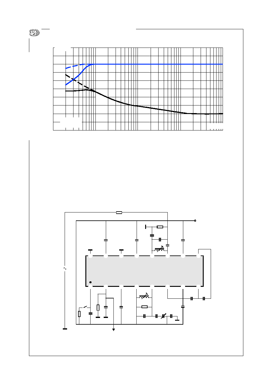
INPUT SENSITIVITY DIAGRAM
10
--6
--80
--60
--40
--20
25
0
10
--5
10
--4
10
--2
10
--3
Noise
S + N
#
#
$
$
EMF (V)
V
oAF
(dB)
Mute ON
#
$
Mute OFF
TEST
AND
APPLICATION INFORMATION
Fig. 4 Test circuit and application for mechanical tuning
Fig. 3
!
!
!
!
!
!
!
!
!
!
!
!
!
!
!
!
!
!
470
pF
330
pF
220
pF
R
S
75
82
pF
68pF
70nH
0.1
µF
10.0k
V
oAF
MUTE
DISABLE
V
P
= +3V
V
iRF
C1
10
nF
3.3nF
3.9nF
180
pF
22
nF
0.1
µF
22
k
1.2k
78nH
18pF
1.8
nF
27
pF
C1 = Toko 2A-15BT-R01
MIKA7088T
EMF
f
( )
RF
9
16
15
14
13
12
11
10
1
2
3
4
5
6
7
8
%
%
%
%
%
%
%
%
%
%
%
%
%
%
%
%
%
%
%
%
%
%
%
%

5
_
MIKA7088T
∑
FM RECEIVER CIRCUIT FOR BATTERY SUPPLY
MI
KRON
JS
C
∑
h
t
tp:
//w
ww.
mikr
o
n
.
r
u
∑
Dec
e
mber 2
2
,
TEST
AND
APPLICATION INFORMATION
(CONTINUED)
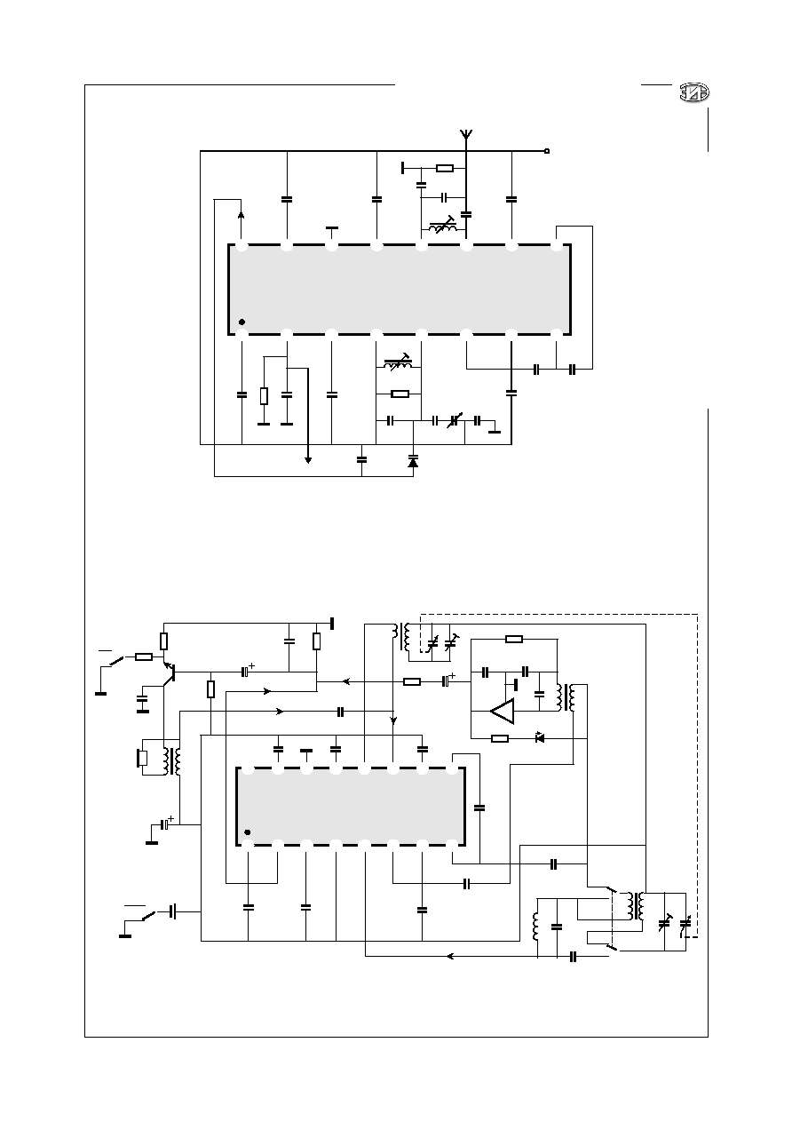
Fig. 5 Application circuit with AFC for mechanical tuning
Fig. 6 AM application circuit
!
!
!
!
!
!
!
!
!
!
!
!
!
!
!
!
470
pF
AFC
330
pF
220
pF
82
pF
68pF
70nH
0.1
µF
10.0k
V
oAF
V
iRF
V
P
= +3V
C1
0.1
µF
C2
D1
BA483
10
nF
3.3nF
3.9nF
180
pF
22
nF
0.1
µF
22
k
1.2k
78nH
18pF
1.8
nF
27
pF
C1 = Toko 2A-15BT-R01
MIKA7088T
9
16
15
14
13
12
11
10
1
2
3
4
5
6
7
8
%
%
%
%
%
%
%
%
%
%
%
%
%
% %
%
%
%
%
%
%
%
%
%
%
%
!
!
!
!
!
!
!
!
!
!
!
!
!
!
!
!
8
9
7
10
6
11
5
12
4
13
3
14
2
15
1
16
MIKA7088T
180
pF
3.9
nF
2.7k
BAW62
*
CC7624
*
CC7624: AM-IF amplifier / demodulator type number WU-xi 742 Fty.
330
pF
33pF
12pF
4.7nF
4.7nF
27
k
22.0k
100k
10k
470
pF
0.1
µF
22µF
1.0µF
10nF
22
nF
47
nF
1.0 µF
10
nF
4.7
nF
33pF
5.1
12
BATTERY
SWITCH
AF
transformer
VOLUME
AF AMPLIFIER
AM ANTENNA
FM ANTENNA
AF
AF
RF
OSCILLATOR
RESONANT
CIRCUIT
ON
+3V
OFF
High
Low
V
P
V
P
Earphone
AM
AM-IF
AM
FM
FM
1.0µF
!
!
!
!
%
%
%
%
%
%
%
%
%
%
%
%
%
%
%
%
%
%
%
%
%
%
%
%
%
%
%
%
%
%
%
%
%
% %
%
%
%
%
%

6
FM RECEIVER CIRCUIT FOR BATTERY SUPPLY
∑
MIKA7088T
Design by Vladimir F.Lityaghin / E-mail: lityaghin@mail.ru / Tel: +7(095)532-64-54
MI
KRON
JS
C
∑
h
t
tp:
//w
ww.
mikr
o
n
.
r
u
∑
Dec
e
mber 2
2
,
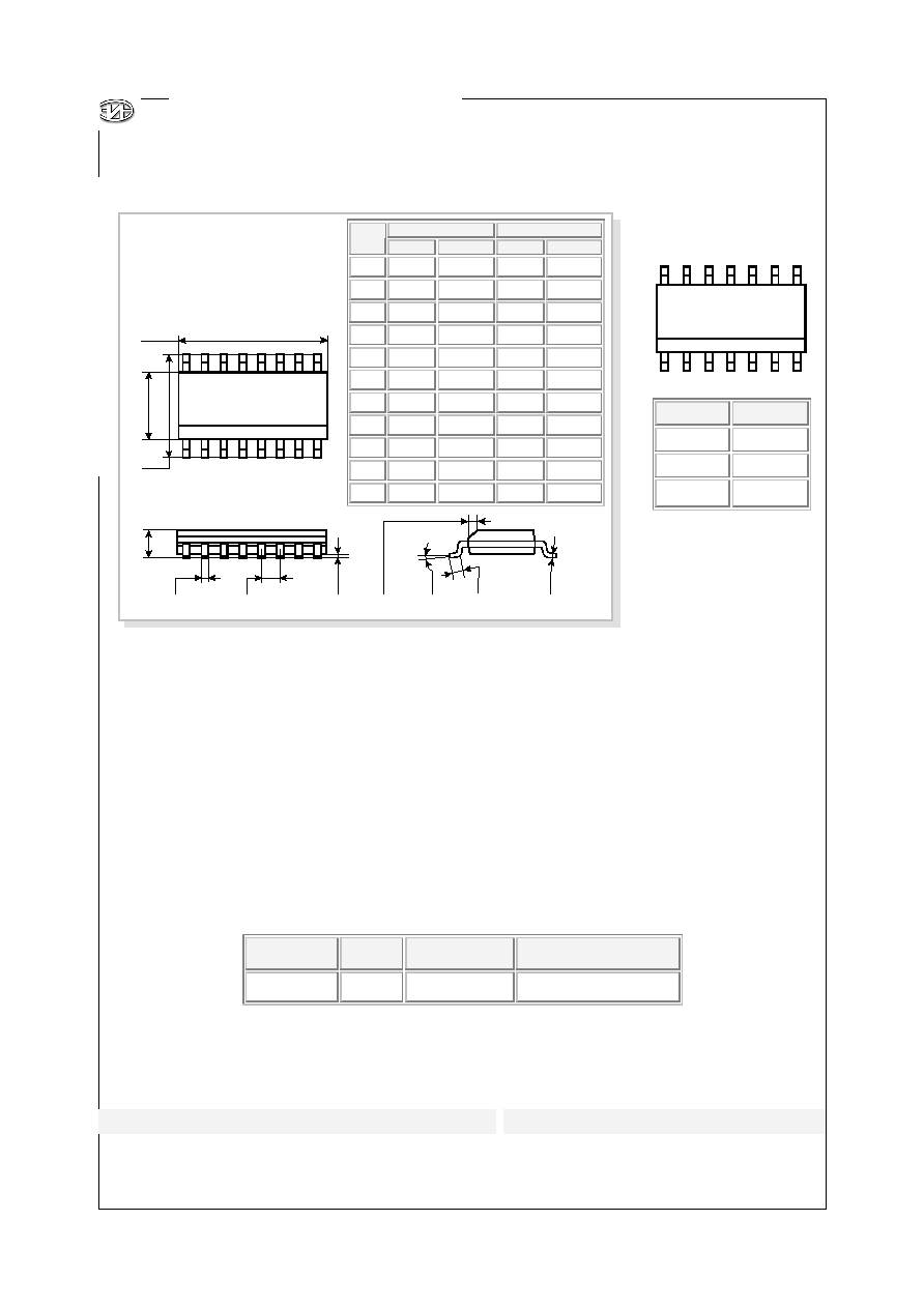
ORDERING INFORMATION
NOTE: T
HE
FORM
OF
PACKING
IS
STIPULATED
IN
THE
CONTRACT
.
DEVICE
PACKAGE
OPERATING
TEMPERATURE
SHIPPING
MIKA7088T
SOP-16
-10∫C to +70∫C
Tube/Rail and Tape/Reel
PHYSICAL DIMENSIONS
&
MARKING DIAGRAM
A
B
C
D
E
F
G
H
J
K
L
1
8
9
16
H
45∫
x
SOP-16
PACKAGE
SOP-16
MARKING DIAGRAM
1
16
MIKA7088T
YYWW/n
ABBREVIATION
ABBREVIATION
EXPANSION
YY
Year
WW
Work Week
n
Assembly
Location
MILLIMETERS
INCHES
DIM
MIN
MAX
MIN
MAX
A
B
C
D
E
F
G
H
J
K
L
9.80
10.00 0.386 0.393
3.80
4.00 0.150
0.157
5.80
6.20
0.229
0.244
1.35
1.75 0.054
0.068
0.35 0.49
0.014
0.019
1.27 BSC 1.27 BSC
0.05
0.05 BSC
0.10 0.25
0.004
0.009
0.25 0.50
0.010
0.019
0∫
7∫
0∫
7∫
0.40
1.25 0.016
0.049
0.19 0.25
0.008
0.009
"
Address: 1
ST
Zapadny Proezd 12, Building 1, Zelenograd, Moscow, Russia, 124460
#
Telephone: +7 (095) 535-23-43; 536-85-44
$
Fax: +7 (095) 530-92-01
%
Email: export@mikron.ru
$
Tel/Fax: +86-755-329-7574
&
Voice: +86-755-329-7573
%
Email: miksz@963.net
MIKRON JSC Head Office
MIKRON ShenZhen Office
The information presented in this Data sheet is believed to be accurate and
reliable. Application circuits shown are typical examples illustrating the
operation of the device.
In the interest of product improvement, MIKRON reserves the right to change
specifications and data without notice and can assume no responsibility for
the use of any information, devices and application circuits described herein.
Reference to products of other manufacturers are solely for convenience and
do not imply total equivalency of design, performance, or otherwise.

