MIK7089F-XX
6 Functions 6 Digit Alarm-
Chronograph Duplexed LCD Watch
Circuit with El Lamp Driver
July 1999 - revised November 2000
Features
∑ Single chip CMOS construction
∑ Drives 6 digit duplexes LCD with 7 day mark, AM/PM
mark, date mark and alarm mark
∑ Colon display
∑ 32,768 Hz Crystal frequency
∑ On-chip oscillator and resistors
∑ On-chip voltage doubler
∑ Low power dissipation
∑ Debounce circuitry on switch inputs
∑ Protection against static discharge
∑ Trimmer capacitor included
∑ Economical solution for EL display
∑ No external component needed for delay function
∑ Min external components in application
Functions
Watch
∑ 6 Function: Month, Date, Day-of-Week, Hour, Minute,
Second
∑ Alarm function with 4 to 5 minute snooze
∑ 6 Digit chronograph: Autoranging after 30 minutes to hour,
minute, second
∑ User selectable 12 hour/24 hour format
∑ Alarm output for melody IC (KS5310, KS5381, KS5318
series)
∑ 4 Year calendar
∑ One touch correction of time error within ±30 seconds
∑ Fast advance for time and alarm time set
∑ Chime on every hour
EL Lamp Driver
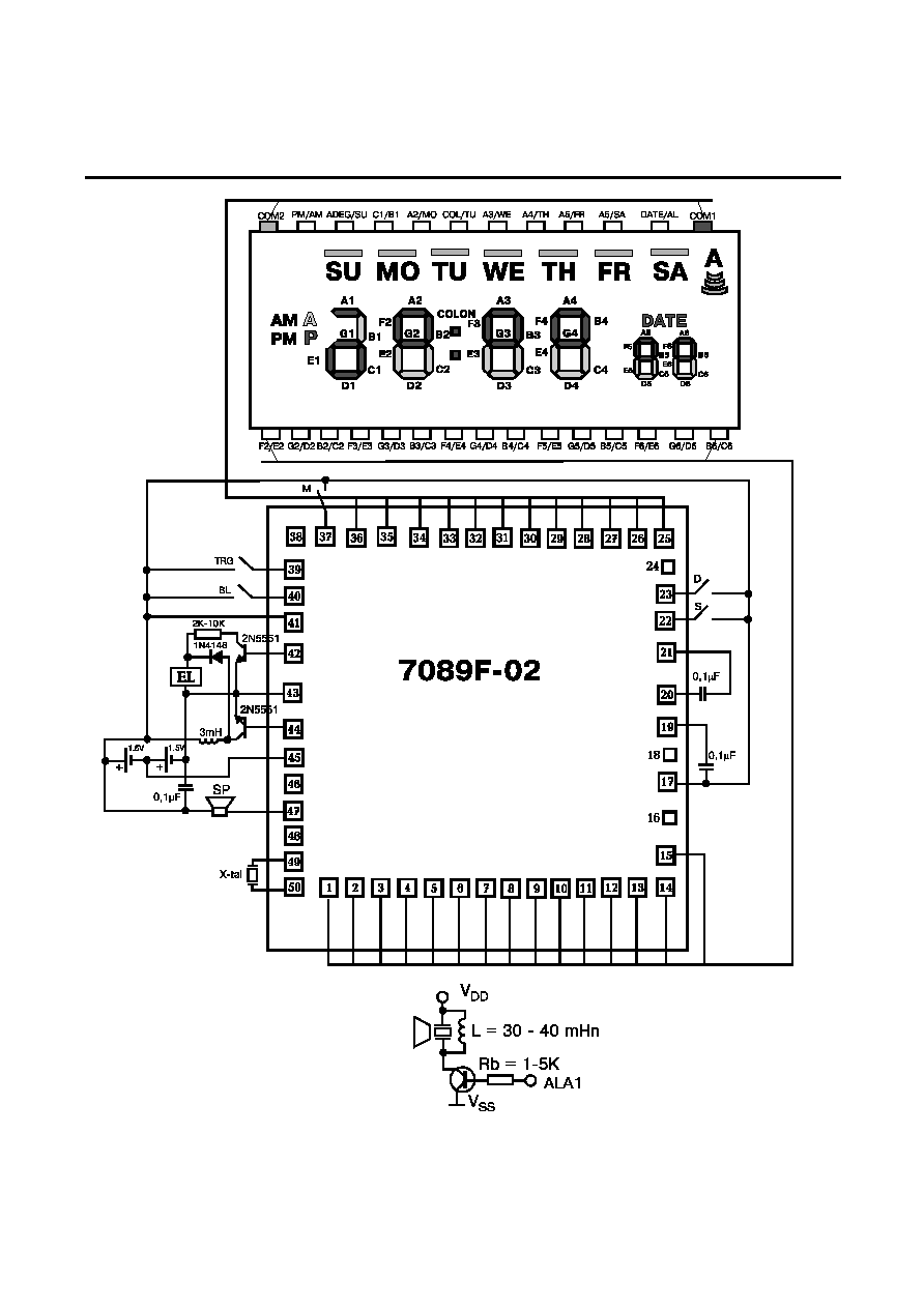
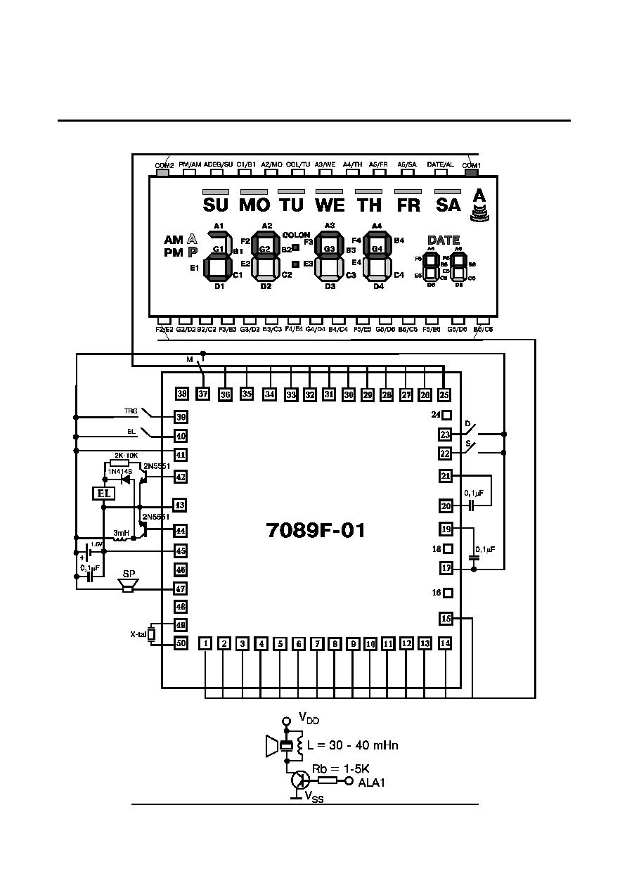
∑ Single 1.5 V or 3.0 V battery operation (mask option)
(7089-01: -1.5 V, 7089-02: -3.0 V)
∑ DC to AC conversion
∑ Built-in delay function
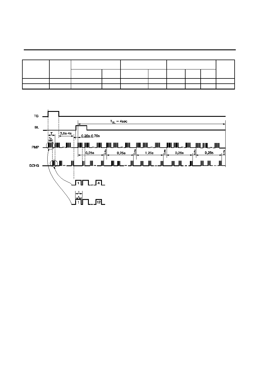
∑ Two independent trigger inputs:
TRG (is active at high)makes EL display for 2,4 or 8
second delay (mask option),
BL (is active at high) makes EL flash without any delay
(See Timing Diagram)
∑ Output frequency-32KHz, 16KHz, 8KHz, 4KHz or 2KHz
(mask option)
∑ PMP duty circle 1/2, 3/4 or 7/8 (mask option)
∑ EL frequency ≠ 1KHz, 512 Hz or 256 Hz (mask option)
Pin Description
N
Pad Name
I/O
Description
N
Pad Name
I/O
Description
1
F2/E2
O
Signal to LCD (Segment)
27
A6
/
SA
O
Signal to LCD (Segment)
2
G2/D2
O
Signal to LCD (Segment)
28
A5/FR
O
Signal to LCD (Segment)
3
B2/C2
O
Signal to LCD (Segment)
29
A4/TH
O
Signal to LCD (Segment)
4
F3/E3
O
Signal to LCD (Segment)
30
A3/WE
O
Signal to LCD (Segment)
5
G3/D3
O
Signal to LCD (Segment)
31
COL/TU
O
Signal to LCD (Segment)
6
B3/C3
O
Signal to LCD (Segment)
32
A2/MO
O
Signal to LCD (Segment)
7
F4/E4
O
Signal to LCD (Segment)
33
C1/B1
O
Signal to LCD (Segment)
8
G4/D4
O
Signal to LCD (Segment)
34
ADEG/SU
O
Signal to LCD (Segment)
9
B4/C4
O
Signal to LCD (Segment)
35
PM/AM
O
Signal to LCD (Segment)
10
F5/E5
O
Signal to LCD (Segment)
36
COM2
O
Signal to LCD (Common)
11
G5/D5
O
Signal to LCD (Segment)
37
M
I
Switch M
12
B5/C5
O
Signal to LCD (Segment)
38
AC
I
Common reset
13
F6/E6
O
Signal to LCD (Segment)
39
TRG
I
Signal EL display (Pull down)
14
G6/D6
O
Signal to LCD (Segment)
40
BL
I
Signal EL flash (Pull down)
15
B6/C6
O
Signal to LCD (Segment)
41
V
DD
Positive Power Supply
16
T1
I
Test Pad1
42
DCHG
O
DC-AC converter
17 V
DD
Positive Power Supply
43
V
EE2
Negative Power Supply for EL
Driver
18
T2
I
Test Pad2
44
PMP
O
DC-AC converter
19 V
EE1
Voltage Doubler Supply
45
V
SS
Negative Power Supply
20
1KO
O
Voltage Doubler Capacitor
46
ALB
O
Sound Converter
21
CAP
I
Voltage Doubler Capacitor
47
ALA 2
O
Sound Converter (Open drain
output)
22
S
I
Switch S
48
ALA1
O
Sound Converter
23
D
I
Switch D
49
OO
O
Oscillator output
24
T3
I
Test Pad 3
50
OI
I
Oscillator input
25
COM1
O
Signal to LCD (Common)
26
DATE/AL
O
Signal to LCD (Segment)
Page 1 of 6

MIK7089F-XX
6 Functions 6 Digit Alarm-
Chronograph Duplexed LCD Watch
Circuit with El Lamp Driver
July 1999 - revised November 2000
Electrical Characteristics MIK7089F-01
(T
a
= 25
o
C, V
DD
= 0 V, V
SS
= V
EE2
= -1.5 V; unless otherwise specified)
Parameter Symbol Test
Condition
Min
Typ
Max
Units
Operating Voltage
V
SS
=V
EE2
1.2
1.5
1.8
V
V
EE1
2.4
3.0
3.6
V
Supply Current
I
DD
Without
Load
2.0
µA
Input High Voltage
V
IH
-0.3
0 V
Input Low Voltage
V
IL
V
SS
V
SS
+0.3
Oscillator Start Voltage
V
OSC
Within 5 sec
1.45
V
Oscillator Frequency
F
OSC
32.768 KHz
DC-DC Conversion Frequency
F
CON
C
1
= C
2
= 0.1
µF
1.024 KHz
LCD Frequency
F
d
32
Hz
Time Stability
T
stb
V
SS
= -1.2
-1.8 V
3
ppm
Switch Debouncing Time
Tdeb
31.25
msec
Output drive Current
I
OH
PMP, V
OH
= -0.7V
DCHG, V
OH
= -0.7V
-1.7 -0.7
-0.2
mA
Output sink Current
I
OL
PMP, V
OL
= -0.9V
DCHG, V
OL
= -0.9V
15
1
mA
I
OL
ALA2,
V
OL
= -0.4V
50
mA
I
OH
ALA1,
V
OH
= -0.7V, Vss = -1.4V
-1.5
mA
I
OL
ALA1,
V
OL
= -0.7V, Vss = -1.4V
1.5
mA
Alarm Driver Current
I
OL
ALB,
V
OL
= -0.7V, Vss = -1.4V
20
µA
Quartz Crystal Parameters: F
= 32768 Hz, C
L
= 12.5
F, C
O
= 1.2
F, C
1
= 3.0
F
F, Rr = 35K
Electrical Characteristics MIK7089F-02
(T
a
= 25
o
C, V
DD
= 0 V, V
SS
= -1.5 V, V
EE2
= -3.0 V; unless otherwise specified)
Characteristic Symbol
Test
Condition Min
Typ
Max
Unit
Operating Voltage
V
SS
1.2
1.5
1.8
V
EE1
2.4
3.0
3.6
V
V
EE2
1.2
3.0
3.6
Supply Current
I
DD
Without
Load
2.0
µA
Input High Voltage
V
IH
-0.3
0
V
Input Low Voltage
V
IL
V
SS
V
SS
+0.3
Oscillator Start Voltage
V
OSC
Within 5 sec
1.45
V
Oscillator Frequency
F
OSC
32.768
KHz
DC-DC Conversion Frequency
F
CON
C
1
= C
2
= 0.1
µF
1.024 KHz
LCD Frequency
F
d
32
Hz
Time Stability
T
stb
V
SS
= -1.2
-1.8 V
3
ppm
Switch Debouncing Time
Tdeb
31.25
msec
Output drive Current
I
OH
PMP, V
OH
= -2.2V
DCHG, V
OH
= -2.2V
-3.4 -1.4
-0.2
mA
Output sink Current
I
OL
PMP, V
OL
= -2.4V
DCHG, V
OL
= -2.4V
15
1
mA
I
OL
ALA2,
V
OL
= -0.4V
50
mA
I
OH
ALA1,
V
OH
= -0.7V, Vss = -1.4V
-1.5
mA
I
OL
ALA1,
V
OL
= -0.7V, Vss = -1.4V
1.5
mA
Alarm Driver Current
I
OL
ALB,
V
OL
= -0.7V, Vss = -1.4V
20
µA
Quartz Crystal Parameters: F
= 32768 Hz, C
L
= 12.5
F, C
O
= 1.2
F, C
1
= 3.0
F
F, Rr = 35K
Page 3 of 6

MIK7089F-XX
6 Functions 6 Digit Alarm-
Chronograph Duplexed LCD Watch
Circuit with El Lamp Driver
July 1999 - revised November 2000
MIK7089F-XX
6 Functions 6 Digit Alarm-
Chronograph Duplexed LCD Watch
Circuit with El Lamp Driver
July 1999 - revised November 2000
Page 5 of 6
Page 5 of 6


