 | –≠–ª–µ–∫—Ç—Ä–æ–Ω–Ω—ã–π –∫–æ–º–ø–æ–Ω–µ–Ω—Ç: MIK7195K | –°–∫–∞—á–∞—Ç—å:  PDF PDF  ZIP ZIP |

MIK7195K
5 Function 3.5 or 4 Digit Watch Circuit
with Alarm and Chime For Duplexed LCD
December 2000
Description
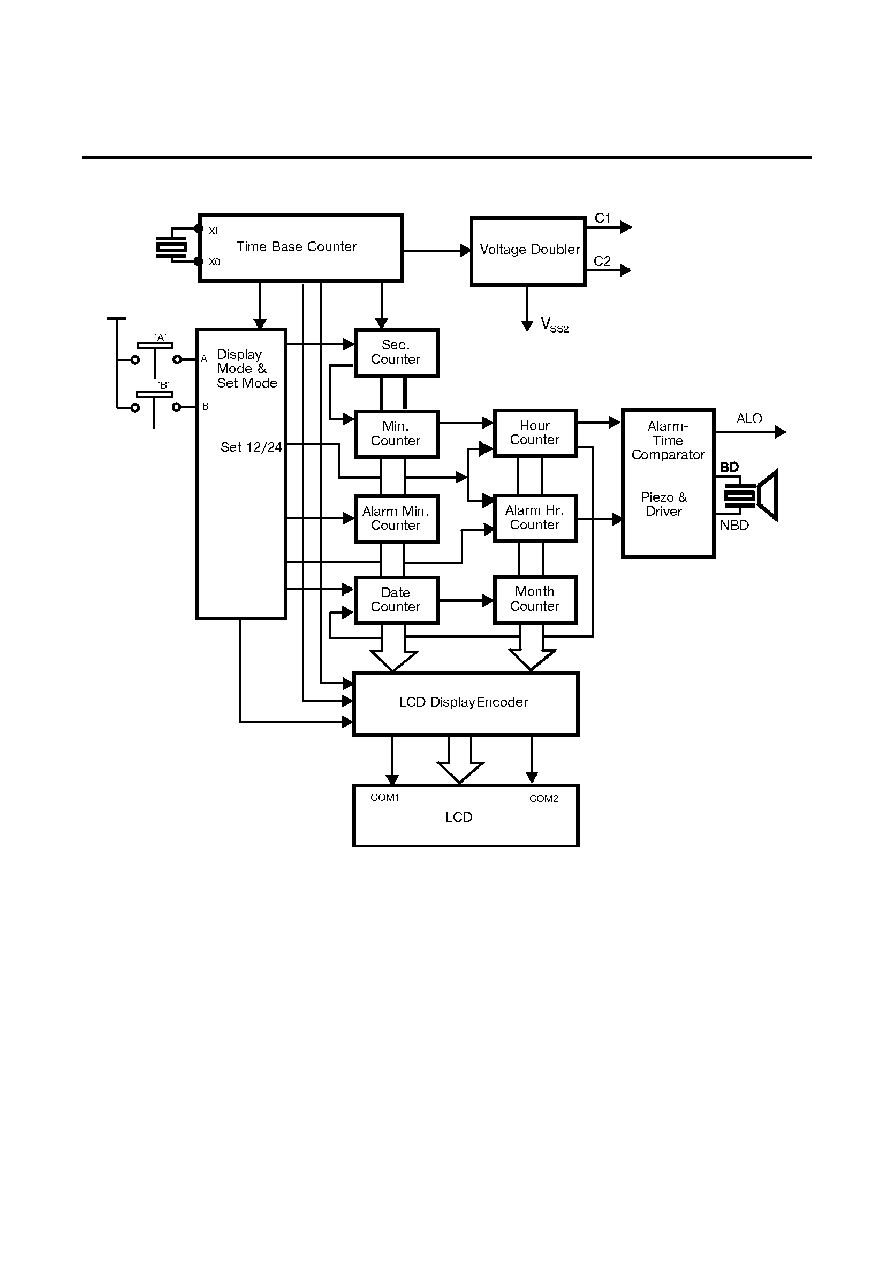
The MIK7195K is a CMOS LSI, with a fundamental frequency of 32.768 kHz, designed for 3 1/2-Digit or 4-Digit 5 function digital
watches with an alarm and chime functions. It contains a 1/2 duty multiplex LCD driver, which display Hours, Minutes, Seconds, Month
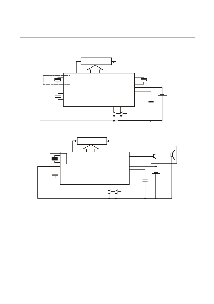
and Date. 12 or 24 hour format can be selected. MIK7195 oscillation circuit starts operating by connecting the 32.768kHz X'tal, built - in
input and output oscillator capacitors (20pF typ). The built-in voltage double start operating when two capacitors (0.1 µF) are connected.
The supply voltage is a single 1.5V. The alarm output circuit can drive the piezo buzzer directly and buzzer transistor drive.
Functions
∑ 5 function watch: hour, minute, second, month and date.
∑ Alarm, Chime enable/disable operation.
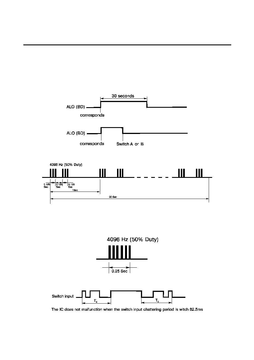
∑ 30-second alarm sound.
∑ Chime on every hour.
∑ 12H cycle; 24H cycle selectable.
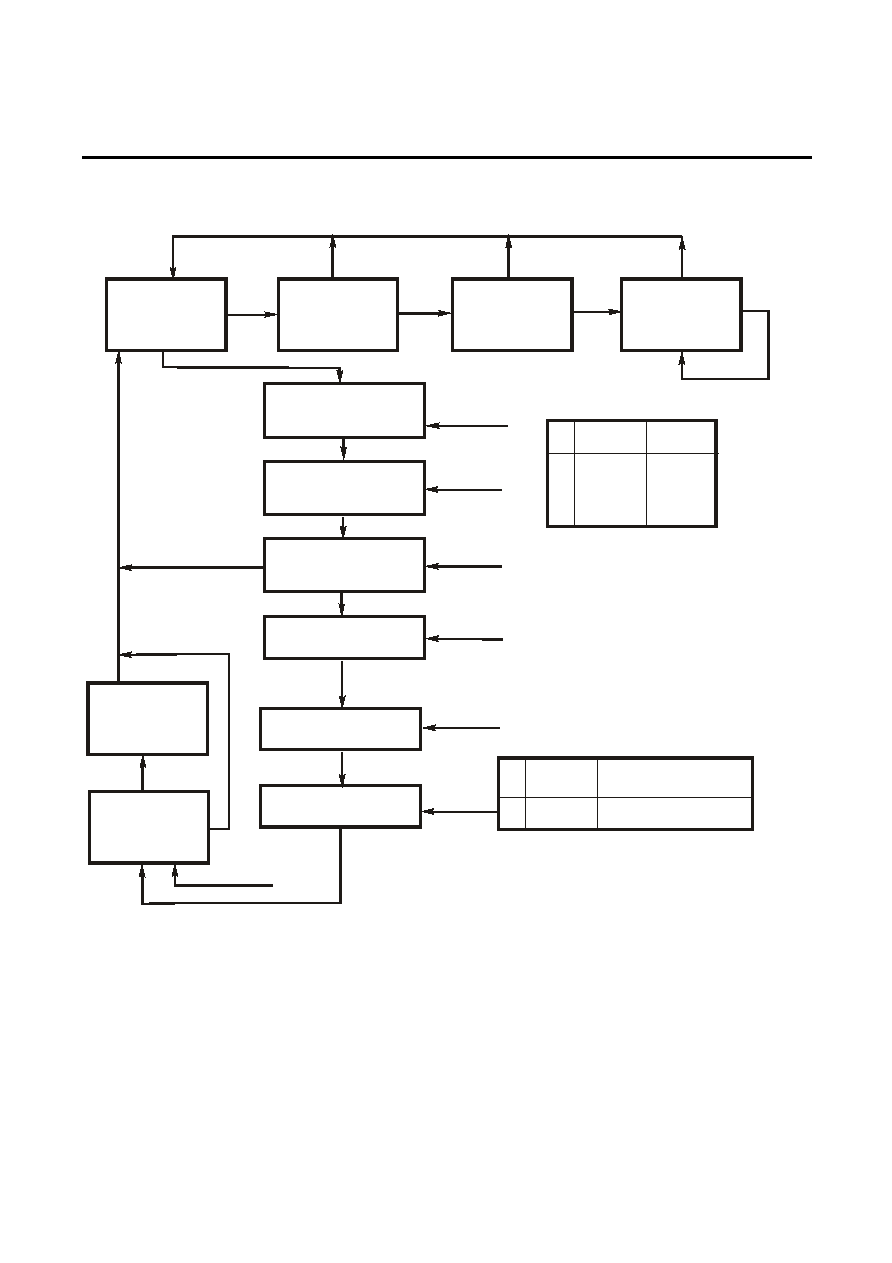
∑ 2-switch sequential operation.
∑ 4 year calendar.
∑ One-touch correction of time error within ±30 seconds.
∑ LCD and ALARM sound test.
Features
∑
Single-chip CMOS construction.
∑
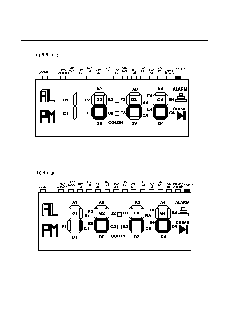
Drives 3 1/2-digit or 4-digit dupplexed LCD with PM/AL-
Time alarm mode, chime mark/ alarm mark.
∑ Low power dissipation (ldd: Max-2.5µA; 1.5V operation)
∑
Colon display.
∑ 32,768 Hz crystal controlled operation.
∑ Single 1.5 V battery operation.
∑ On-chip capacitive voltage doubler.
∑ Debounce circuitry on switch inputs.
∑ Protection against static discharge.
∑ Built-in crystal oscillator input and output capacitors.
∑ Buzzer transistor drive.
Electrical Characteristics
(T
a
= 25
0
C, V
ss1
=-1.5V, V
dd
=0V, FX'tal=32,768kHz; unless otherwise specified)
Parameter Symbol
Test
Condition
Min
Typ
Max
Units
Operating voltage 1
|V
SS1
|
1.2
1.5 1.8 V
Operating voltage 2
|V
SS2
|
2.4
3.0 3.6 V
Supply current
I
dd
without load, V
SS1
=-1.5V (watch mode)
2.5
µA
Input low voltage
V
il
V
SS1
V
SS1
+0.3
V
Input high voltage
V
ih
V
dd
-0.3 V
dd
V
Input current
I
ih
V
ih
= V
dd
10
µA
Alarm
output current
(BD, NBD)
I
ol
I
oh
V
ol
= -0.7V
V
SS1
= -1.4V
V
oh
= -0.7V
1.5
-1.5
mA
Alarm
output current
(ALO)
I
ol
I
oh
V
ol
= -0.7V
V
SS1
= -1.4V
V
oh
= -0.7V
200
-200
µA
Oscillator start voltage
|V
OSC
|
within 5 sec.
1.45
V
DC-DC conversion
frequency
F
con
C1=C2=0.1µF
1.024 Hz
LDC frequency
F
d
32
Hz
Time stability
T
stb
V
SS1
=-1.3
˜ -1.8V
3
ppm
Switch debouncing time
T
o
62.5
msec
Page 1 of 8

MIK7195K
5 Function 3.5 or 4 Digit Watch Circuit
with Alarm and Chime For Duplexed LCD
December 2000
Block Diagram
Page 2 of 8

MIK7195K
5 Function 3.5 or 4 Digit Watch Circuit
with Alarm and Chime For Duplexed LCD
December 2000
Pad Description
Pad No
Pad Name
I/O
Description
1
CHIME/AL mark
O
LCD Segment Drive
2
C4/B4
O
LCD Segment Drive
3
G4/A4
O
LCD Segment Drive
4
E4/F4
O
LCD Segment Drive
5
C3/B3
O
LCD Segment Drive
6
G3/AD3
O
LCD Segment Drive
7
E3/F3
O
LCD Segment Drive
8
D4/COL
O
LCD Segment Drive
9
C2/B2
O
LCD Segment Drive
10
G2/A2
O
LCD Segment Drive
11
E2/F2
O
LCD Segment Drive
12
D2/B1
O
LCD Segment Drive
13
C1/ADEG1
O
LCD Segment Drive
14
PM/AL mode
O
LCD Segment Drive
15 NC
16
COM2
O
Common Signal 2
17
XI
I
Oscillator Input with Built-in Capacitor
18
X0
O
Oscillator Output with Built-in Capacitor
19
Vdd
I
Positive Power Supply
20
C1
I
Voltage Double Capacitor Positive
21
C2
I
Voltage Double Capacitor Negative
22 B
I Switch
B
23 T1
I Test
Pad1
24 T2
I Test
Pad2
25 T3
I Test
Pad3
26 V
SS2
(-1.5V)
I
Voltage Double Supply
27 V
dd
(+1.5V)
I
Positive Power Supply
28 NC
-
29 V
SS1
(0V) I
Ground
30 A
I Switch
A
31
NBD
O
Piezo Buzzer Driving
32
BD
O
Piezo Buzzer Driving
33 ALO
O Transistor
Drive
34 COM1
O Common
Signal1
Page 3 of 8

MIK7195K
5 Function 3.5 or 4 Digit Watch Circuit
with Alarm and Chime For Duplexed LCD
December 2000
LCD Format
Page 4 of 8

MIK7195K
5 Function 3.5 or 4 Digit Watch Circuit
with Alarm and Chime For Duplexed LCD
December 2000
Setting Sequence and Switch Operation
A Alarm Chime
0 OFF OFF
1 ON OFF
2 ON ON
3 OFF ON
A 12 ~ 11 12 HOUR MODE
P 12 ~ 11
H 0 ~ 23 24 HOUR MODE
Normal
Display
HR : MIN***
AL&CH EN/DIS
AL-HOUR*: AL-MIN*
AL mode
Alarm Hour Set
AL-HOUR: A/P/H
AL mode
Alarm Minute Set
: AL-MIN*
AL mode
Month Set
MONTH
Date Set
DATE
A
A
A
A
A
A
A
Advance
Advance
Advance
* Flashing at a 2 Hz rate
** Colon normally flashes at a 1Hz rate
and when min is adjusted the colon
stops, and second counter is reset.
*** Colon normaly flashes at a 1 Hz
+1 for each depression and
advances at a 2Hz rate with
a continuous depression: When
alarm and chime functions are
enabled, their marks appear
except in month/date and
second display state.
Advance:
Advance
Advance
Advance
Advance
A
If the MIN
is not adjusted
If A switch is
pressed in the
alarm time
setting mode
B
B
B
B
B
B
B
B
B
A
A
A
A
2
3
sec
2 3
sec
Hour Set
HOUR: A/P/H***
Hour State
HOUR : MIN
Minute Set
**
MIN
Month/Date
Display
MON DATE
Second
Display
:SEC
Alarm Time
Display
HOUR : MIN
AL mode
Page 5 of 8

MIK7195K
5 Function 3.5 or 4 Digit Watch Circuit
with Alarm and Chime For Duplexed LCD
December 2000
Application Circuit
1. Standard connection diagram
XO
XI
Vdd
Vss1
Vss2
LDC
C1
0.1 F
µ
C2
X'tal
Built - in gate
capacitors use
A
0.1 F
µ
1.55V
$
+
B
COM1
SEGMENT
COM2
BD
NBD
Piezo
2. Example of using buzzer transistor drive
X0
XI
Vdd
Vss1
Vss2
LDC
C1
0.1 F
µ
C2
X'tal
A
0.1 F
µ
1.55V
$
+
B
COM1
SEGMENT
COM2
Buzzer transistor
drive
Built - in gate
capacitors use
ALO
Buzzer
Quartz crystal parameters:
Fp = 32768 Hz, C
L
= 12.5 pF, C
0
=1.2 pF,
C1 = 3.0 µF, Rr = 35 KOm.
Page 6 of 8

MIK7195K
5 Function 3.5 or 4 Digit Watch Circuit
with Alarm and Chime For Duplexed LCD
December 2000
Alarm Functions
Alarm signal is output from ALO, BD and NBD pins, when the time corresponds to the alarm time during alarm standby mode (ALARM
= ON). The alarm time corresponds to the 12H/24H cycle of the time function.
Alarm functions operate under normal mode and setting modes.
Alarm Signal Output Specifications
Output Length
When the time corresponds to the alarm time, alarm signal start and stops automatically after 30 seconds.
Alarm Output Wave form (ALO, BD, NBD)
Chime Function
Alarm buzzer sounds for 0.25 second in chime enable mode when the minute of normal time reaches zero. In other words, the chime
function generates a 0.25 second burst of sound for every hour on the hour.
Chime Signal (ALO, BD, NBD)
Switch Chattering
Page 7 of 8

MIK7195K
5 Function 3.5 or 4 Digit Watch Circuit
with Alarm and Chime For Duplexed LCD
December 2000
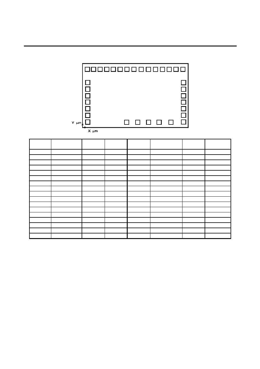
Pad Location MIK7195K
18
32
17
33
25
24
23
22
21
29
19
31
10
11
3
4
5
6
7
8
9
2
12
27
28
14
1
13
26
16
34
15
0
20
30
Chip Size:
2.26 mm x 1.5 mm
Pad Size:
100 m x 100 m,
140 m steps
Substrate to Vdd
µ
µ
µ
Pad Location Coordinates
Pad No
Pad Name
X(mm)
Y(µm)
Pad No
Pad Name
X(µm)
Y(µm)
1 CHIME/AL
mark
2114 1349
18
X0
146
786
2 C4/B4
1974
1349
19 Vdd 146 626
3 G4/A4
1834
1349
20 C1 146 466
4 E4/F4
1694
1349
21 C2 146
306
5 C3/B3
1554
1349
22
B 146 146
6 G3/AD3
1414
1349
23
T1 1119 146
7 E3/F3
1274
1349
24 T2 1279
146
8 D4/COL
1134
1349
25
T3 1439 146
9 C2/B2 994
1349
26 V
SS2
1594
146
10 G2/A2 854
1349
27 Vdd 1754 146
11 E2/F2 714
1349
28 NC 2114
146
12 D2/B1 574
1349
29 V
SS1
2114
306
13 C1/ADEG1 434 1349 30
A
2114 466
14 PM/AL
mode 294 1349 31
NBD
2114 626
15 NC 154
1349
32 BD 2114
786
16 COM2 146
1106
33 ALO 2114 946
17 XI 146
946
34
COM1
2114
1101
Page 8 of 8

