1
MI
KRON
JS
C
∑
ht
t
p
:
//ww
w
.mikron.ru
∑
16 J
UN
E
20
0
3
MIK78XX series
∑
1A POSITIVE-VOLTAGE REGULATORS
DATA SHEET
16 J
UNE
2003
N
O
. 00011
R
EV
1-03
CONTENTS
Page
GENERAL DESCRIPTION
1
FEATURES
1
INTERNAL BLOCK DIAGRAM
2
PIN DESCRIPTION
2
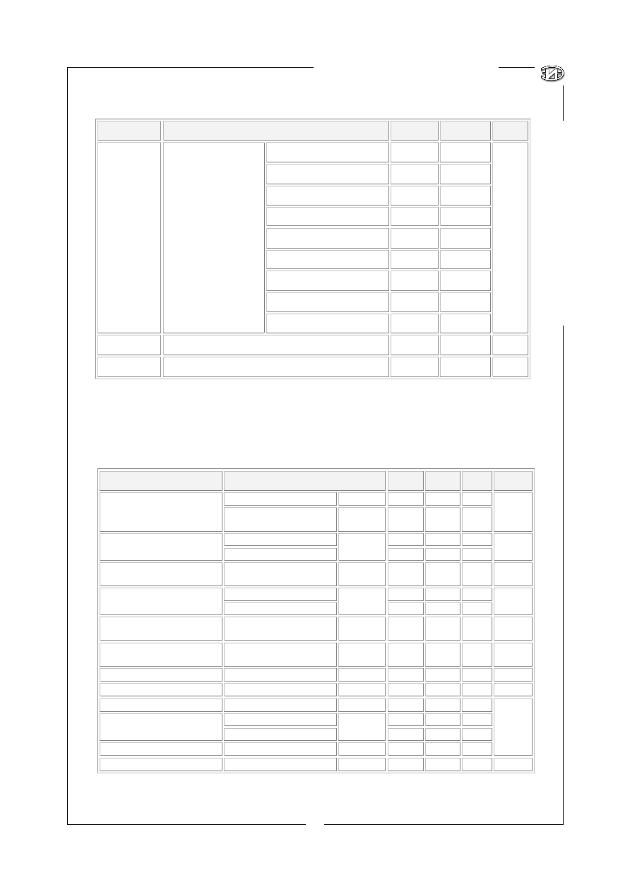
ABSOLUTE MAXIMUM RATINGS
2
FREE-AIR TEMPERATURE DISSIPATION
DERATING CURVE
2
CASE TEMPERATURE DISSIPATION DERATING
CURVE
2
RECOMMENDED OPERATING CONDITIONS
3
ELECTRICAL CHARACTERISTICS
3
MIK 7805
3
MIK 7806
4
MIK 7808
4
MIK 7809
5
MIK 7810
5
MIK 7812
6
MIK 7815
6
CONTENTS
Page
MIK 7818
7
MIK 7824
7
TYPICAL APPLICATIONS
8
FIXED-OUTPUT REGULATOR
8
POSITIVE REGULATOR IN NEGATIVE
CONFIGURATION
8
ADJUSTABLE-OUTPUT REGULATOR
8
CURRENT REGULATOR
8
REGULATED DUAL SUPPLY
8
OUTPUT POLARITY-REVERSAL-PROTECTION
CIRCUIT
8
REVERSE-BIAS-PROTECTION CIRCUIT
8
PHYSICAL DIMENSIONS AND MARKING
DIAGRAMS
9
TO-220
-3
9
TO-263
-3
9
ORDERING INFORMATION
10
GENERAL DESCRIPTION
This series of fixed-voltage monolithic integrated-
circuit voltage regulators is designed for a wide range
of applications. These applications include on-card
regulation for elimination of noise and distribution
problems associated with single-point regulation. In
addition, they can be used with power-pass elements
to make high-current voltage regulators. Each of
these regulators can deliver up to 1.5 A of output
current. The internal limiting and thermal shutdown
features of these regulators make them essentially
immune to overload.
FEATURES
∑
3-Terminal Regulators
∑
Output Current Up to 1.5 A
∑
No External Components
∑
Internal Thermal Overload Protection
∑
High Power Dissipation Capability
∑
Internal Short-Circuit Current Limiting
∑
Output Transistor Safe-Area Compensation
REPLACEMENT of:
µA78
XX
KA78
XX
LM78
XX
MC78
XX
MIK78xx series
POSITIVE-VOLTAGE REGULATORS

Design by Vladimir F.Lityaghin / E-mail: lityaghin@mail.ru / Tel: +7(095)532-64-54
MI
KRON
JS
C
∑
h
ttp
:
/
/www.
m
i
kr
o
n
.
r
u
∑
16 J
UN
E
2
003
1A POSITIVE-VOLTAGE REGULATORS
∑
MIK78XX series
2
INTERNAL BLOCK DIAGRAM
ABSOLUTE MAXIMUM RATINGS
Over operating free-air temperature range, unless otherwise noted.
NOTE: For operation
above 25
∞
C free-air or
90
∞
C case temperature,
refer to Figures 1 and 2.
To avoid exceeding the
design maximum virtual
junction temperature,
these ratings should not be
exceeded. The built-in
t h e r m a l o v e r l o a d
p r o t e c t i o n m a y b e
activated at power levels
slightly above or below the
rated dissipation.
CASE TEMPERATURE
DISSIPATION DERATING CURVE
FREE-AIR TEMPERATURE
DISSIPATION DERATING CURVE
2000
1800
1600
1400
1200
1000
800
600
400
200
0
25
50
T
A
- FREE-AIR TEMPERATURE (∫C)
Derating factor = 16mW/∫C
R
JA
64 ∫C/W
M
A
X
I
MU
M C
O
N
T
I
N
U
O
U
S
D
I
SSI
P
A
T
I
O
N
(
m
W)
75
100
125
150
0
2
4
6
8
10
12
14
16
25
50
T
C
- CASE TEMPERATURE (∫C)
Derating factor = 0.25 W/∫C
above 90∫C
R
JC
4 ∫C/W
M
A
X
I
MU
M C
O
N
T
I
N
U
O
U
S
DI
SSI
P
A
T
I
O
N
(
W
)
75
100
125
150
Fig. 1
Fig. 2
!
!
!
!
!
!
!
!
!
!
!
"
"
"
"
INPUT
1
3
2
OUTPUT
COMMON
CURRENT
GENERATOR
REFERENCE
VOLTAGE
ERROR
AMPLIFIER
THERMAL
PROTECTION
SERIES
PASS
ELEMENT
SOA
PROTECTION
STARTING
CIRCUIT
PIN DESCRIPTION
MIK78-xx
CT
TO-220-3
1 -- INPUT
2 -- COMMON
3 -- OUTPUT
TAB
-- COMMON
MIK78-xx
CD2T
TO-263-3
1 -- INPUT
2 -- COMMON
3 -- OUTPUT
TAB
-- COMMON
TAB
2
1
3
TAB
2
1
3
SYMBOL
PARAMETER
MAXIMUM
UNIT
MIK7824 40
V
IN
Input voltage
All others
35
V
P
D
Continuous total dissipation at 25
∞
C free-
air temperature
2
P
D
Continuous total dissipation at (or below)
25
∞
C case temperature
15
W
T
A
Operating free-air temperature range
T
C
Operating case temperature range
T
J
Operating virtual junctions temperature
range
0 to 150
T
STG
Storage temperature range
-65 to 150
T
L
Lead temperature 1.6 mm (1/16 inch)
from case for 10 seconds
260
∞
C
NOTE:
Stresses above those listed
under ´Absolute Maximum
Ratingsª may cause permanent
damage to the device. These
are stress ratings only and
functional operation of the
device at these or any other
conditions above those
indicated in the operation
sections of the specifications is
not implied.
Exposure to Absolute Maximum
Rating conditions for extended
periods may affect device
reliability.
3
MI
KRON
JS
C
∑
ht
t
p
:
//ww
w
.mikron.ru
∑
16 J
UN
E
20
0
3
MIK78XX series
∑
1A POSITIVE-VOLTAGE REGULATORS
RECOMMENDED OPERATING CONDITIONS
SYMBOL
PARAMETER
MIN
MAX
UNIT
MIK7805
7.0 25.0
MIK7806
8.0 25.0
MIK7808
10.5 25.0
MIK7809
11.5 27.0
MIK7810
12.5 28.0
MIK7812
14.5 30.0
MIK7815
17.5 30.0
MIK7818
21.0 33.0
V
IN
Input voltage
MIK7824
27.0 38.0
V
I
OUT
Output current
1.5
A
T
J
Operating virtual junction temperature
0
125
∞
C
ELECTRICAL CHARACTERISTICS MIK7805
Electrical characteristics at specified virtual junction temperature, V
IN
= 10V, I
OUT
= 500mA (unless otherwise noted)
* Pulse testing techniques are used to maintain the junction temperature as close to the ambient temperature as possible.
Thermal effects must be taken into account separately.
** This specification applies only for dc power dissipation permitted by absolute maximum ratings.
PARAMETER
TEST CONDITIONS*
MIN
TYP
MAX
UNIT
25
∞
C
4.8 5 5.2
Output voltage**
I
OUT
= 5mA to 1A,
V
IN
= 7V to 20V, P
15W
0
∞
C to
125
∞
C
4.75 5 5.25
V
V
IN
= 7V to 25V
3
100
Input regulation
V
IN
= 8V to 12V
25
∞
C
1
50
mV
Ripple rejection
V
IN
= 8V to 18V,
f = 120Hz
0
∞
C to
125
∞
C
62 78 dB
I
OUT
= 5mA to 1.5A
15
100
Output regulation
I
OUT
= 250mA to 750mA
25
∞
C
5
50
mV
Output resistance
f = 1KHz
0
∞
C to
125
∞
C
0.017
Temperature coefficient of
output voltage
I
OUT
= 5mA
0
∞
C to
125
∞
C
-1.1
mV/
∞
C
Output noise voltage
f = 10 Hz to 100 KHz
25
∞
C
40 µV
Dropout voltage
I
OUT
= 1A
25
∞
C
2.0 V
Bias current
25
∞
C
4.2
8
V
IN
= 7V to 25V
1.3
Bias current change
I
OUT
= 5mA to 1A
0
∞
C to
125
∞
C
0.5
Short-circuit output current
25
∞
C
750
mA
Peak output current
25
∞
C
2.2 A

Design by Vladimir F.Lityaghin / E-mail: lityaghin@mail.ru / Tel: +7(095)532-64-54
MI
KRON
JS
C
∑
h
ttp
:
/
/www.
m
i
kr
o
n
.
r
u
∑
16 J
UN
E
2
003
1A POSITIVE-VOLTAGE REGULATORS
∑
MIK78XX series
4
ELECTRICAL CHARACTERISTICS MIK7806
Electrical characteristics at specified virtual junction temperature, V
IN
= 11V, I
OUT
= 500mA (unless otherwise noted)
PARAMETER
TEST CONDITIONS*
MIN
TYP
MAX
UNIT
25
∞
C
5.75 6 6.25
Output voltage**
I
OUT
= 5mA to 1A,
V
IN
= 8V to 21V, P
15W
0
∞
C to
125
∞
C
5.7 6 6.3
V
V
IN
= 8V to 25V
5
120
Input regulation
V
IN
= 9V to 13V
25
∞
C
1.5 60
mV
Ripple rejection
V
IN
= 9V to 19V,
f = 120Hz
0
∞
C to
125
∞
C
59 75 dB
I
OUT
= 5mA to 1.5A
14
120
Output regulation
I
OUT
= 250mA to 750mA
25
∞
C
4 60
mV
Output resistance
f = 1KHz
0
∞
C to
125
∞
C
0.019
Temperature coefficient of
output voltage
I
OUT
= 5mA
0
∞
C to
125
∞
C
-0.8 mV/
∞
C
Output noise voltage
f = 10 Hz to 100 KHz
25
∞
C
45 µV
Dropout voltage
I
OUT
= 1A
25
∞
C
2.0 V
Bias current
25
∞
C
4.3 8
V
IN
= 8V to 25V
1.3
Bias current change
I
OUT
= 5mA to 1A
0
∞
C to
125
∞
C
0.5
Short-circuit output current
25
∞
C
550
mA
Peak output current
25
∞
C
2.2 A
ELECTRICAL CHARACTERISTICS MIK7808
Electrical characteristics at specified virtual junction temperature, V
IN
= 14V, I
OUT
= 500mA (unless otherwise noted)
* Pulse testing techniques are used to maintain the junction temperature as close to the ambient temperature as possible.
Thermal effects must be taken into account separately.
** This specification applies only for dc power dissipation permitted by absolute maximum ratings.
PARAMETER
TEST CONDITIONS*
MIN
TYP
MAX
UNIT
25
∞
C
7.7 8 8.3
Output voltage**
I
OUT
= 5mA to 1A,
V
IN
= 10.5V to 23V, P
15W
0
∞
C to
125
∞
C
7.6 8 8.4
V
V
IN
= 10.5V to 25V
6
160
Input regulation
V
IN
= 11V to 17V
25
∞
C
2
80
mV
Ripple rejection
V
IN
= 11.5V to 21.5V,
f = 120Hz
0
∞
C to
125
∞
C
55 72 dB
I
OUT
= 5mA to 1.5A
12
160
Output regulation
I
OUT
= 250mA to 750mA
25
∞
C
4
80
mV
Output resistance
f = 1KHz
0
∞
C to
125
∞
C
0.016
Temperature coefficient of
output voltage
I
OUT
= 5mA
0
∞
C to
125
∞
C
-0.8
mV/
∞
C
Output noise voltage
f = 10 Hz to 100 KHz
25
∞
C
52 µV
Dropout voltage
I
OUT
= 1A
25
∞
C
2.0 V
Bias current
25
∞
C
4.3 8
V
IN
= 10.5V to 25V
1
Bias current change
I
OUT
= 5mA to 1A
0
∞
C to
125
∞
C
0.5
Short-circuit output current
25
∞
C
450
mA
Peak output current
25
∞
C
2.2 A

5
MI
KRON
JS
C
∑
ht
t
p
:
//ww
w
.mikron.ru
∑
16 J
UN
E
20
0
3
MIK78XX series
∑
1A POSITIVE-VOLTAGE REGULATORS
ELECTRICAL CHARACTERISTICS MIK7810
Electrical characteristics at specified virtual junction temperature, V
IN
= 17V, I
OUT
= 500mA (unless otherwise noted)
* Pulse testing techniques are used to maintain the junction temperature as close to the ambient temperature as possible. Thermal
effects must be taken into account separately.
** This specification applies only for dc power dissipation permitted by absolute maximum ratings.
ELECTRICAL CHARACTERISTICS MIK7809
Electrical characteristics at specified virtual junction temperature, V
IN
= 16V, I
OUT
= 500mA (unless otherwise noted)
PARAMETER
TEST CONDITIONS*
MIN
TYP
MAX
UNIT
25
∞
C
8.65 9 9.35
Output voltage**
I
OUT
= 5mA to 1A,
V
IN
= 11.5V to 24V, P
15W
0
∞
C to
125
∞
C
8.55 9 9.45
V
V
IN
= 11.5V to 27V
7
180
Input regulation
V
IN
= 13V to 19V
25
∞
C
2
90
mV
Ripple rejection
V
IN
= 12V to 22V, f= 120Hz
0
∞
C to
125
∞
C
55 70 dB
I
OUT
= 5mA to 1.5A
12
180
Output regulation
I
O
= 250mA to 750mA
25
∞
C
4
90
mV
Output resistance
f= 1KHz
0
∞
C to
125
∞
C
0.018
Temperature coefficient of
output voltage
I
OUT
= 5mA
0
∞
C to
125
∞
C
-1.0 mV/
∞
C
Output noise voltage
f= 10 Hz to 100 KHz
25
∞
C
60 µV
Dropout voltage
I
OUT
= 1A
25
∞
C
2.0 V
Bias current
25
∞
C
4.3 8
V
IN
= 11.5V to 27V
1
Bias current change
I
OUT
= 5mA to 1A
0
∞
C to
125
∞
C
0.5
Short-circuit output current
25
∞
C
400
mA
Peak output current
25
∞
C
2.2 A
PARAMETER
TEST CONDITIONS*
MIN
TYP
MAX
UNIT
25
∞
C
9.6 10 10.4
Output voltage**
I
OUT
= 5mA to 1A,
V
IN
= 12.5V to 25V, P
15W
0
∞
C to
125
∞
C
9.5 10 10.5
V
V
IN
= 12.5V to 28V
25
∞
C
7
200
Input regulation
V
IN
= 14V to 20V
2
100
mV
Ripple rejection
V
IN
= 13V to 23V,
f = 120Hz
0
∞
C to
125
∞
C
55 71 dB
I
OUT
= 5mA to 1.5A
25
∞
C
12
200
Output regulation
I
OUT
= 250mA to 750mA
4
100
mV
Output resistance
f = 1KHz
0
∞
C to
125
∞
C
0.018
Temperature coefficient of
output voltage
I
OUT
= 5mA
0
∞
C to
125
∞
C
-1.0 mV/
∞
C
Output noise voltage
f = 10 Hz to 100 KHz
25
∞
C
70 µV
Dropout voltage
I
OUT
= 1A
25
∞
C
2.0 V
Bias current
25
∞
C
4.3 8
V
IN
= 12.5V to 28V
0
∞
C to
125
∞
C
1
Bias current change
I
OUT
= 5mA to 1A
0.5
Short-circuit output current
25
∞
C
400
mA
Peak output current
25
∞
C
2.2 A