 | –≠–ª–µ–∫—Ç—Ä–æ–Ω–Ω—ã–π –∫–æ–º–ø–æ–Ω–µ–Ω—Ç: MIK79L05A | –°–∫–∞—á–∞—Ç—å:  PDF PDF  ZIP ZIP |

Replacement of
µA79L00
MIK79L00
100 mA Negative
Voltage Regulator
September 1995-revised September 2002
Description
This series of fixed-voltage monolithic integrated-circuit voltage regulators is designed for a wide range of applications. These
applications include on-card regulation for elimination of noise and distribution problems associated with single-point regulation. In
addition, they can be used with power-pass elements to make high-current voltage regulators. Each of these regulators can deliver up to
100 mA of output current. The internal limiting and termal shutdown features of these regulators make them essentially immune to
overload. When used as a replacement for a Zener diode-resistor combination, an effective improvement in output impedance can be
obtained together with lower-bias current.
Features
∑
3-Terminal Regulators
∑
Output Current Up to 100 mA
∑
No External Components
∑
Internal Thermal Overload Protection
∑
Internal Short-Circuit Limiting
Package information
Package TO-92
(top view)
C
I
O
Absolute Maximum Ratings
over operating temperature range (unless otherwise noted)
Parameter
MIK79L05A
thru
MIK79L08A
MIK79L12A
THRU
MIK79L18A
MIK79L24A Units
Input voltage
-30
-35
-40
V
Operating free-air, case, or virtual junction
temperature range
0 to 150
0 to 150
0 to 150
Storage temperature range
-65 to 150
-65 to 150
-65 to 150
Lead temperature 1.6 mm (1/16 inch) from case
for 10 seconds
260 260 260
∞C
Recommended Operating Conditions
Parameter Min
Max
Units
MIK79L05A -7
-20
MIK79L06A -8
-20
MIK79L08A -10.5
-23
MIK79L12A -14.5
-27
MIK79L15A -17.5
-30
MIK79L18A -20.5
-33
Input voltage V
I
MIK79L24A -27
-38
V
Output current, I
O
100
mA
Operating virtual junction temperature, T
J
0
125
∞C
Device Selection Guide
Output Voltage
Device
-5 V
MIK79L05A
-6 V
MIK79L06A
-8 V
MIK79L08A
-12 V
MIK79L12A
-15 V
MIK79L15A
-18 V
MIK79L18A
-24 V
MIK79L24A
Page 1 of 5

Replacement of
µA79L00
MIK79L00
100 mA Negative
Voltage Regulator
September 1995-revised September 2002
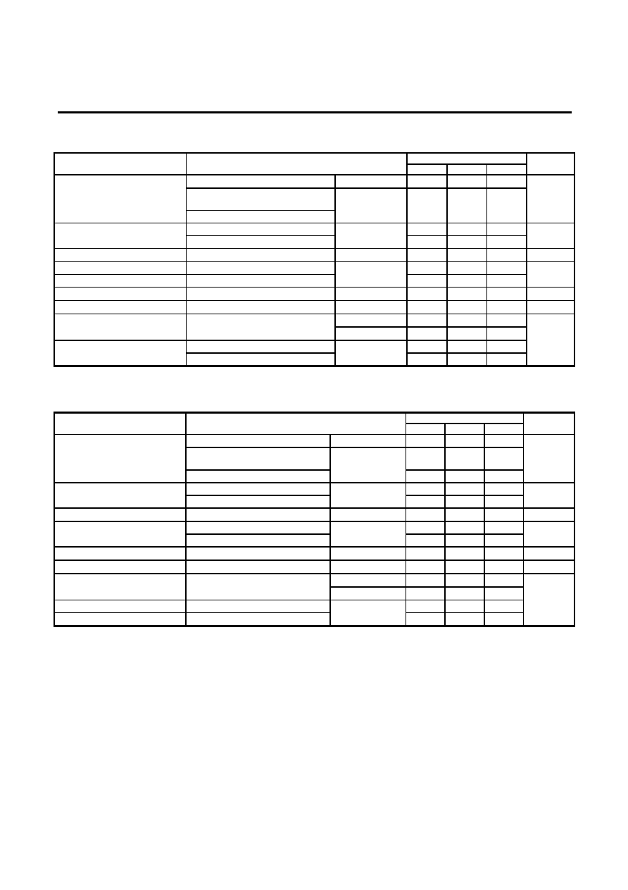
Electrical characteristics MIK79L05A
Electrical characteristics at specified virtual junction temperature, V
I
= -10V,I
O
= 40mA (unless otherwise noted)
MIK79L05A
Parameter Test
conditions*
Min Typ Max
Units
25
∞C
-4.8 -5 -5.2
I
O
= 1mA to 40 mA, V
I
= -7V to -20V
-4.75
-5.25
Output voltage**
I
O
= 1mA to 70mA,
0
∞C to 125∞C
-4.75 -5.25
V
V
I
= -7V to -20V
15
150
Input regulation
V
I
= -8V to -20V
25
∞C
12
100
mV
Ripple rejection
V
I
= -8V to -18V, f= 120Hz
25
∞C
41 49 dB
I
O
= 1mA to 100mA
20
60
Output regulation
I
O
= 1mA to 40mA
25
∞C
10 30
mV
Output noise voltage
f= 10Hz to 100 KHz
25
∞C
40 µV
Dropout voltage
25
∞C
1.7 V
25
∞C
6
Bias current
125
∞C
5.5
V
I
= -8V to -20V
1.5
Bias current change
I
O
= 1mA to 40mA
0
∞C to 125∞C
0.1
mA
Electrical characteristics MIK79L06A
Electrical characteristics at specified virtual junction temperature, V
I
= -11V,I
O
= 40mA (unless otherwise noted)
MIK79L06A
Parameter Test
conditions*
Min Typ Max
Units
25
∞C
-5.75 -6 -6.25
I
O
= 1mA to 40 mA, V
I
= -8V to -20V
Output voltage**
I
O
= 1mA to 70mA,
0
∞C to 125∞C
-5.7
-6.3
V
V
I
= -8V to -20V
20
175
Input regulation
V
I
= -9V to -20V
25
∞C
15
125
mV
Ripple rejection
V
I
= -9V to -19V, f= 120Hz
25
∞C
40 48 dB
I
O
= 1mA to 100mA
21
80
Output regulation
I
O
= 1mA to 40mA
25
∞C
11 40
mV
Output noise voltage
f= 10Hz to 100 KHz
25
∞C
44 µV
Dropout voltage
25
∞C
1.7 V
25
∞C
6
Bias current
125
∞C
5.5
V
I
= -9V to -20V
1.5
Bias current change
I
O
= 1mA to 40mA
0
∞C to 125∞C
0.1
mA
* Pulse testing techniques are used to maintain the junction temperature as close to the ambient temperature as possible. Thermal
effects must be taken into account separately. All characteristics are measured with a 0.33µF capacitor across the input and a 0.1 µF
capacitor across the output.
** This specification applies only for dc power dissipation permitted by absolute maximum ratings.
Page 2 of 5
Replacement of
µA79L00
MIK79L00
100 mA Negative
Voltage Regulator
September 1995-revised September 2002
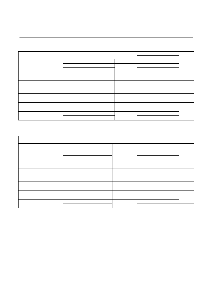
Electrical characteristics MIK79L08A
Electrical characteristics at specified virtual junction temperature, V
I
= -14V,I
O
= 40mA (unless otherwise noted)
MIK79L08A
Parameter Test
conditions*
Min Typ Max
Units
25
∞C
-7.7 -8 -8.3
I
O
= 1mA to 40 mA, V
I
= -10.5V to -
23V
Output voltage**
I
O
= 1mA to 70mA,
0
∞C to 125∞C
-7.6
-8.4
V
V
I
= -10,5V to ≠23V
42
200
Input regulation
V
I
= -11V to -23V
25
∞C
36
150
mV
Ripple rejection
V
I
= -11V to -21V, f= 120Hz
25
∞C
37 46 dB
Output regulation
I
O
= 1mA to 100mA
30
100
I
O
= 1mA to 40mA
25
∞C
15 50
mV
Output noise voltage
f= 10Hz to 100 KHz
25
∞C
54 µV
Dropout voltage
25
∞C
1.7 V
25
∞C
6
Bias current
125
∞C
5.5
V
I
= -11V to -23V
1.5
Bias current change
I
O
= 1mA to 40mA
0
∞C to 125∞C
0.1
mA
Electrical characteristics MIK79L12A
Electrical characteristics at specified virtual junction temperature, V
I
= -19V,I
O
= 40mA (unless otherwise noted)
MIK79L12A
Parameter Test
conditions*
Min Typ Max
Units
25
∞C
-11.5 -12 -12.5
I
O
= 1mA to 40mA, V
I
= -14.5V to -
27V
-11.4 -12.6
Output voltage**
I
O
= 1mA to 70mA
0
∞C to 125∞C
-11.4 -12.6
V
V
I
= -14.5V to -27V
50
250
Input regulation
V
I
= -16V to -27V
25
∞C
40
200
mV
Ripple rejection
V
I
= -15V to -25V, f= 120Hz
0
∞C to 125∞C
37 42
dB
I
O
= 1mA to 100mA
24
100
Output regulation
I
O
= 1mA to 40mA
25
∞C
15 50
mV
Output noise voltage
f= 10Hz to 100 KHz
25
∞C
80 µV
Dropout voltage
25
∞C
1.7 V
25
∞C
6.5
Bias current
125
∞C
6
Bias current change
V
I
= -16V to -27V
1.5
I
O
= 1mA to 40mA
0
∞C to 125∞C
0.1
mA
* Pulse testing techniques are used to maintain the junction temperature as close to the ambient temperature as possible. Thermal
effects must be taken into account separately. All characteristics are measured with a 0.33µF capacitor across the input and a 0.1 µF
capacitor across the output.
** This specification applies only for dc power dissipation permitted by absolute maximum ratings.
Page 3 of 5
Replacement of
µA79L00
MIK79L00
100 mA Negative
Voltage Regulator
September 1995-revised September 2002
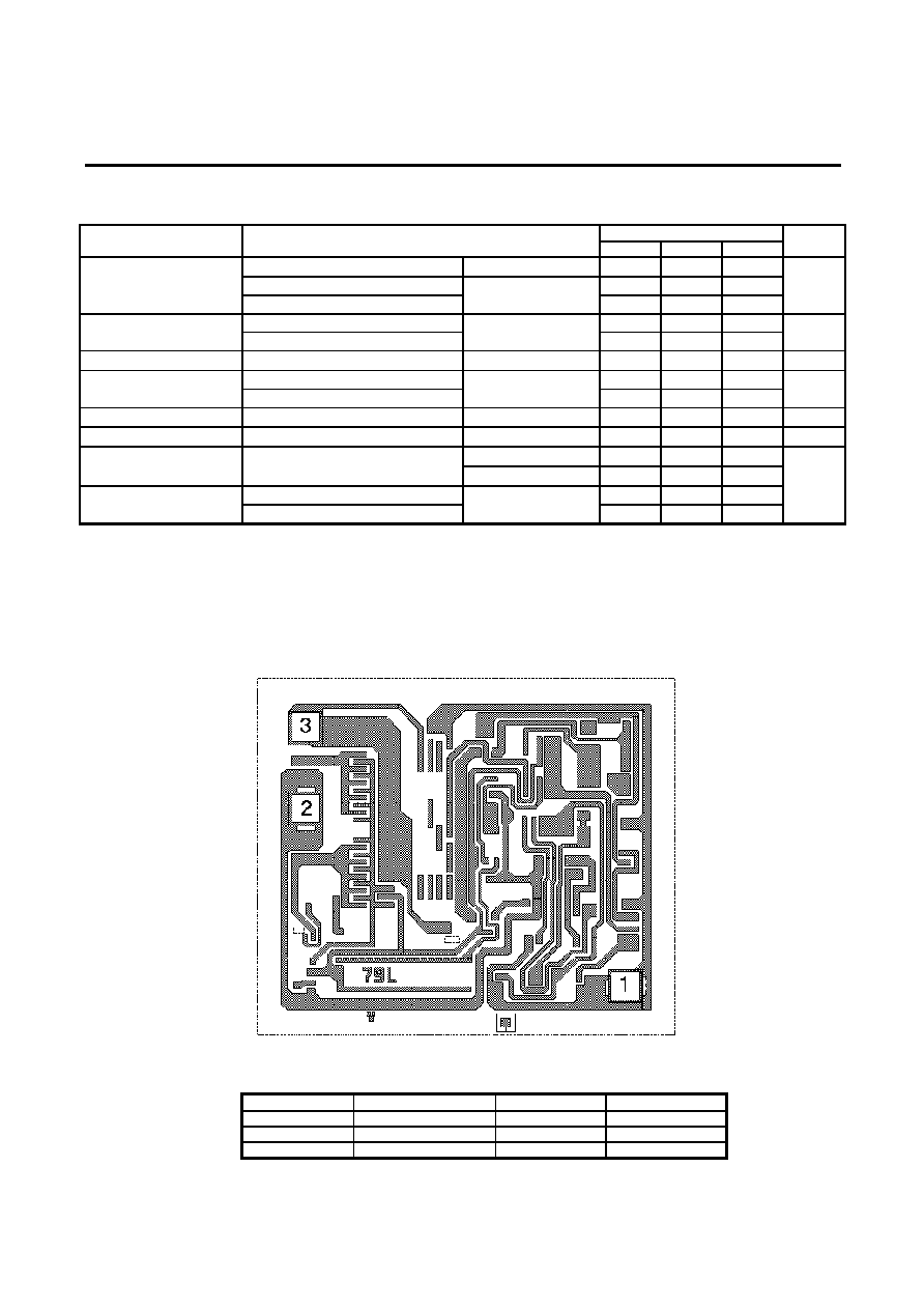
Electrical characteristics MIK79L15A
Electrical characteristics at specified virtual junction temperature, V
I
= -23V,I
O
= 40mA (unless otherwise noted)
MIK79L15A
Parameter Test
conditions*
Min Typ Max
Units
25
∞C
-14.4 -15 -15.6
I
O
= 1mA to 40mA, V
I
= -17.5V to -30V
-14.25
-15.75
Output voltage**
I
O
= 1mA to 70mA
0
∞C to 125∞C
-14.25 -15.75
V
V
I
= -17.5V to -30V
65
300
Input regulation
V
I
= -20V to -30V
25
∞C
50
250
mV
Ripple rejection
V
I
= -18.5V to -28.5V, f= 120Hz
0
∞C to 125∞C
34 39 dB
I
O
= 1mA to 100mA
25
150
Output regulation
I
O
= 1mA to 40mA
25
∞C
15 75
mV
Output noise voltage
f= 10Hz to 100 KHz
25
∞C
90 µV
Dropout voltage
25
∞C
1.7 V
25
∞C
6.5
Bias current
125
∞C
6
V
I
= -20V to -30V
1.5
Bias current change
I
O
= 1mA to 40mA
0
∞C to 125∞C
0.1
mA
Electrical characteristics MIK79L18A
Electrical characteristics at specified virtual junction temperature, V
I
= -26V,I
O
= 40mA (unless otherwise noted)
MIK79L18A
Parameter Test
conditions*
Min Typ Max
Units
25
∞C
-17.3 -18 -18.7
I
O
= 1mA to 40mA,
V
I
= -20.5V to -33V
-17.1 -18.9
Output voltage**
I
O
= 1mA to 70mA
0
∞C to 125∞C
-17.1 -18.9
V
V
I
= -20.5V to -33V
70
325
Input regulation
V
I
= -21V to -33V
25
∞C
60
275
mV
Ripple rejection
V
I
= -23V to -33V, f= 120Hz
0
∞C to 125∞C
33 48 dB
I
O
= 1mA to 100mA
27
170
Output regulation
I
O
= 1mA to 40mA
25
∞C
19 85
mV
Output noise voltage
f= 10Hz to 100 KHz
25
∞C
150 µV
Dropout voltage
25
∞C
1.7 V
25
∞C
6.5
Bias current
125
∞C
6
V
I
= -21V to -33V
1.5
mA
Bias current change
I
O
= 1mA to 40mA
0
∞C to 125∞C
0.1
* Pulse testing techniques are used to maintain the junction temperature as close to the ambient temperature as possible. Thermal
effects must be taken into account separately. All characteristics are measured with a 0.33µF capacitor across the input and a 0.1 µF
capacitor across the output.
** This specification applies only for dc power dissipation permitted by absolute maximum ratings.
Page 4 of 5
Replacement of
µA79L00
MIK79L00
100 mA Negative
Voltage Regulator
September 1995-revised September 2002
Electrical characteristics MIK79L24A
Electrical characteristics at specified virtual junction temperature, V
I
= -33V,I
O
= 40mA (unless otherwise noted)
MIK79L24A
Parameter Test
conditions*
Min Typ Max
Units
25
∞C
-23 -24 -25
I
O
= 1mA to 40mA, V
I
= -27V to -38V
-22.8
-25.2
Output voltage**
I
O
= 1mA to 70mA
0
∞C to 125∞C
-22.8 -25.2
V
V
I
= -27V to -38V
90
350
Input regulation
V
I
= -28V to -38V
25
∞C
75
300
mV
Ripple rejection
V
I
= -29V to -35V, f= 120Hz
0
∞C to 125∞C
31 47 dB
I
O
= 1mA to 100mA
40
200
Output regulation
I
O
= 1mA to 40mA
25
∞C
25
100
mV
Output noise voltage
f= 10Hz to 100 KHz
25
∞C
200 µV
Dropout voltage
25
∞C
1.7 V
25
∞C
6.5
Bias current
125
∞C
6
V
I
= -28V to -38V
1.5
Bias current change
I
O
= 1mA to 40mA
0
∞C to 125∞C
0.1
mA
* Pulse testing techniques are used to maintain the junction temperature as close to the ambient temperature as possible. Thermal
effects must be taken into account separately. All characteristics are measured with a 0.33µF capacitor across the input and a 0.1 µF
capacitor across the output.
** This specification applies only for dc power dissipation permitted by absolute maximum ratings.
Pad Location MIK79L00
Chip size 1.15 x 1.35 mm
Pad Location Coordinates
Pad N
Pad Name
X (
µm) Y
(
µm)
1 Ground
1150
115
2 Input
115
690
3 Output
115
950
Page 5 of 5