 | –≠–ª–µ–∫—Ç—Ä–æ–Ω–Ω—ã–π –∫–æ–º–ø–æ–Ω–µ–Ω—Ç: 18KWR0327 | –°–∫–∞—á–∞—Ç—å:  PDF PDF  ZIP ZIP |

Pre-production
Mimix Broadband, Inc., 10795 Rockley Rd., Houston, Texas 77099
Tel: 281.988.4600 Fax: 281.988.4615 mimixbroadband.com
Characteristic Data and Specifications are subject to change without notice.
©
2005 Mimix Broadband, Inc.
Export of this item may require appropriate export licensing from the U.S. Government. In purchasing these parts, U.S. Domestic customers accept
their obligation to be compliant with U.S. Export Laws.
General Description
Mimix Broadband
'
s 13.0-25.0 GHz GaAs MMIC
fundamental image reject Kowari mixer can be used as
an up- or down-converter. The device has a conversion
loss of 7.0 dB with 20.0 dB image rejection across the
band. I and Q mixer outputs are provided and an external
90 degree hybrid is required to select the desired
sideband. This MMIC uses Mimix Broadband
'
s 2
µ
m GaAs
HBT device model technology, and is based upon
electron beam lithography to ensure high repeatability
and uniformity. The chip has surface passivation to
protect and provide a rugged part with backside via
holes and gold metallization to allow either a conductive
epoxy or eutectic solder die attach process. This device is
well suited for Millimeter-wave Point-to-Point Radio,
LMDS, SATCOM and VSAT applications.
+20 dBm
+20 dBm
-65 to +165
O
C
-55 to +125
O
C
Absolute Maximum Ratings
Fundamental Image Reject Mixer
GaAs HBT Technology
7.0 dB Conversion Loss
20.0 dB Image Rejection
100% On-Wafer RF Testing
100% Visual Inspection to MIL-STD-883
Method 2010
Features
Input Power (RF Pin)
Input Power (IF Pin)
Storage Temperature (Tstg)
Operating Temperature (Ta)
Chip Device Layout
Page 1 of 6
13.0-25.0 GHz GaAs MMIC
Image Reject Mixer
18KWR0327
Electrical Characteristics (Ambient Temperature T = 25
o
C)
Units
GHz
GHz
GHz
GHz
dB
dB
dB
dB
dBm
dBc
dB
dB
dB
dBm
Min.
15.0
13.0
11.0
DC
-
-
-
-
-
-
-
-
-
-
Typ.
-
-
-
-
10.0
10.0
TBD
7.0
+16.0
20.0
TBD
TBD
TBD
+12.0
Max.
25.0
25.0
29.0
4.0
-
-
-
-
-
-
-
-
-
-
Parameter
Frequency Range (RF) Upper Side Band
Frequency Range (RF) Lower Side Band
Frequency Range (LO)
Frequency Range (IF)
RF Return Loss (S11)
IF1/IF2 Return Loss (S22)
LO Return Loss (S33)
Conversion Loss (S21)
LO Input Drive (P
LO
)
Image Rejection
Isolation LO/RF
Isolation LO/IF
Isolation RF/IF
Output Third Order Intercept (OIP3)
November 2005 - Rev 21-Nov-05
Pre-production
Mimix Broadband, Inc., 10795 Rockley Rd., Houston, Texas 77099
Tel: 281.988.4600 Fax: 281.988.4615 mimixbroadband.com
Characteristic Data and Specifications are subject to change without notice.
©
2005 Mimix Broadband, Inc.
Export of this item may require appropriate export licensing from the U.S. Government. In purchasing these parts, U.S. Domestic customers accept
their obligation to be compliant with U.S. Export Laws.
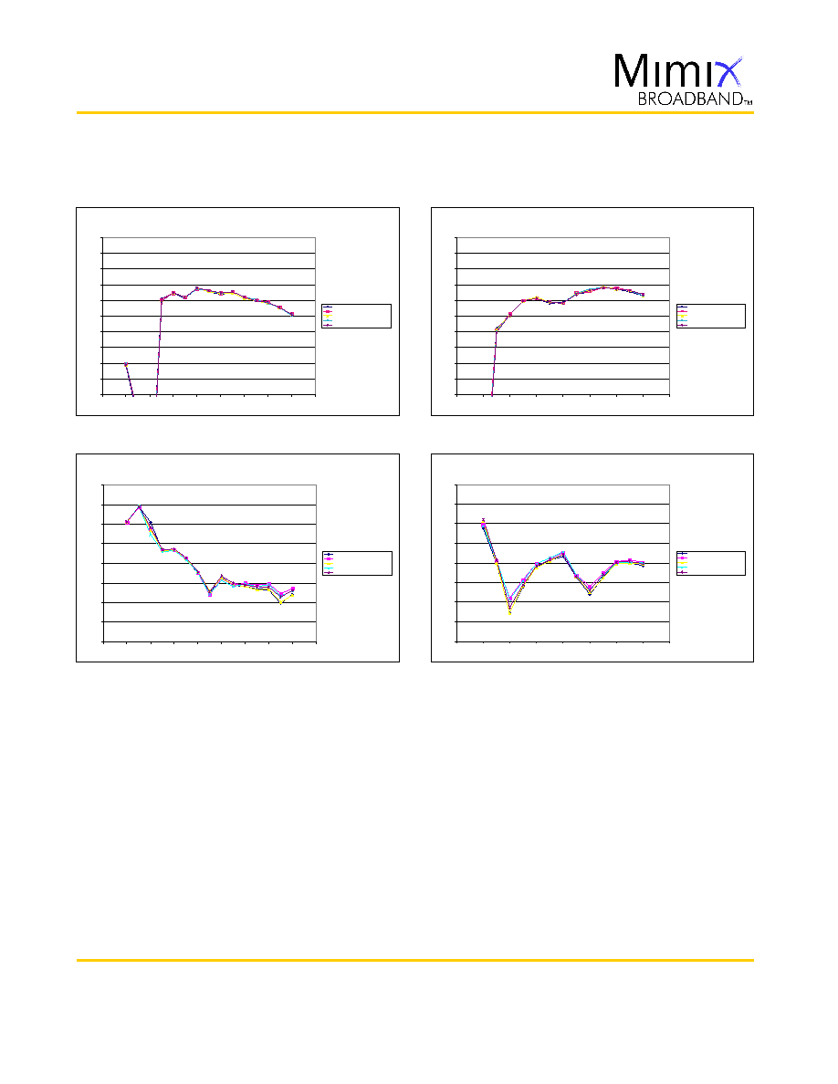
Mixer Measurements
Page 2 of 6
18KWR0327
2902_0327: USB con versi on gain vs. RF freq
L O=16dBm, IF=2GHz, RF=-20dBm
-20
-18
-16
-14
-12
-10
-8
-6
-4
-2
0
10
12
14
16
18
20
22
24
26
28
RF freq (GHz)
U
S
B
c
o
n
v
er
si
o
n
g
a
i
n
(
d
B
)
2902_0327_R2C2_USB_16022004_1623.mix
2902_0327_R5C5_USB_16022004_1634.mix
2902_0327_R3C3_USB_16022004_1630.mix
2902_0327_R2C6_USB_16022004_1627.mix
2902_0327_R6C2_USB_16022004_1637.mix
2902_0327: LSB conversion gain vs. RF freq
LO =16dBm, IF=2GHz, RF=-20dBm
-20
-18
-16
-14
-12
-10
-8
-6
-4
-2
0
8
10
12
14
16
18
20
22
24
RF f re q ( GHz)
LS
B
c
o
nv
e
r
s
i
on
ga
i
n
(
d
B
)
2902_0327_R2C2_LSB_16022004_1642.mix
2902_0327_R5C5_LSB_16022004_1652.mix
2902_0327_R3C3_LSB_16022004_1648.mix
2902_0327_R2C6_LSB_16022004_1645.mix
2902_0327_R6C2_LSB_16022004_1655.mix
2902_0327: image
rejection vs.
RF freq
LO =16dBm, IF=2GHz, RF=-20dBm
-40
-35
-30
-25
-20
-15
-10
-5
0
10
12
14
16
18
20
22
24
26
28
RF freq (GHz)
USB i
m
a
g
e r
e
j
e
ct
i
o
n
(
d
B
c
)
2902_0327_R2C2_USB_16022004_1623.mix
2902_0327_R5C5_USB_16022004_1634.mix
2902_0327_R3C3_USB_16022004_1630.mix
2902_0327_R2C6_USB_16022004_1627.mix
2902_0327_R6C2_USB_16022004_1637.mix
2902_0327: image
rejection vs.
RF freq
LO =16dBm, IF=2GHz, RF=-20dBm
-40
-35
-30
-25
-20
-15
-10
-5
0
8
10
12
14
16
18
20
22
24
RF f re q ( GHz)
LSB i
m
a
g
e r
e
j
e
ct
i
o
n
(
d
B
c
)
2902_0327_R2C2_LSB_16022004_1642.mix
2902_0327_R5C5_LSB_16022004_1652.mix
2902_0327_R3C3_LSB_16022004_1648.mix
2902_0327_R2C6_LSB_16022004_1645.mix
2902_0327_R6C2_LSB_16022004_1655.mix
13.0-25.0 GHz GaAs MMIC
Image Reject Mixer
November 2005 - Rev 21-Nov-05
Pre-production
Mimix Broadband, Inc., 10795 Rockley Rd., Houston, Texas 77099
Tel: 281.988.4600 Fax: 281.988.4615 mimixbroadband.com
Characteristic Data and Specifications are subject to change without notice.
©
2005 Mimix Broadband, Inc.
Export of this item may require appropriate export licensing from the U.S. Government. In purchasing these parts, U.S. Domestic customers accept
their obligation to be compliant with U.S. Export Laws.
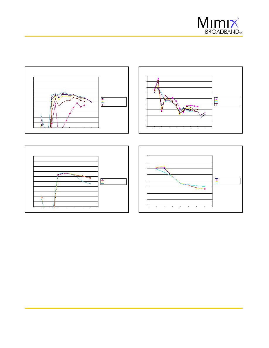
Mixer Measurements (cont.)
Page 3 of 6
18KWR0327
2902_0327: USB con versi on gain vs. RF freq
LO=varied, I F=2GHz, RF=-20dBm
-20
-18
-16
-14
-12
-10
-8
-6
-4
-2
0
10
12
14
16
18
20
22
24
26
28
RF freq (GHz)
U
S
B
c
o
n
v
er
si
o
n
g
a
i
n
(
d
B
)
2902_0327_R3C3_USB_16022004_1615_15dBm.mix
2902_0327_R3C3_USB_16022004_1728_10dBm.mix
2902_0327_R3C3_USB_16022004_1724_14dBm.mix
2902_0327_R3C3_USB_16022004_1720_17dBm.mix
2902_0327_R3C3_USB_16022004_1619_16dBm.mix
2902_0327_R3C3_USB_16022004_1732_12dBm.mix
2902_0327: image
rejection vs. RF freq
LO=varied, IF =2GHz, RF=-20dBm
-40
-35
-30
-25
-20
-15
-10
-5
0
5
10
12
14
16
18
20
22
24
26
28
RF freq (GHz)
USB i
m
a
g
e r
e
j
e
ct
i
o
n
(
d
B
c
)
2902_0327_R3C3_USB_16022004_1615_15dBm.mix
2902_0327_R3C3_USB_16022004_1728_10dBm.mix
2902_0327_R3C3_USB_16022004_1724_14dBm.mix
2902_0327_R3C3_USB_16022004_1720_17dBm.mix
2902_0327_R3C3_USB_16022004_1619_16dBm.mix
2902_0327_R3C3_USB_16022004_1732_12dBm.mix
2902_0327: USB con versi on gain vs. RF freq
LO=16dBm, IF=2GHz, RF =varied
-20
-18
-16
-14
-12
-10
-8
-6
-4
-2
0
10
12
14
16
18
20
22
24
26
RF freq (GHz)
U
S
B
c
o
nv
e
r
s
i
on
ga
i
n
(
d
B
)
2902_0327_R3C3_USB_16022004_1735_-15dBm.mix
2902_0327_R3C3_USB_16022004_1740_-5dBm.mix
2902_0327_R3C3_USB_16022004_1738_-10dBm.mix
2902_0327_R3C3_USB_16022004_1744_0dBm.mix
2902_0327: image
rejection vs. RF freq
LO=16dBm, IF=2GHz, RF =varied
-40
-35
-30
-25
-20
-15
-10
-5
0
10
12
14
16
18
20
22
24
26
RF freq (GHz)
USB i
m
a
g
e r
e
j
e
ct
i
o
n
(
d
B
c
)
2902_0327_R3C3_USB_16022004_1735_-15dBm.mix
2902_0327_R3C3_USB_16022004_1740_-5dBm.mix
2902_0327_R3C3_USB_16022004_1738_-10dBm.mix
2902_0327_R3C3_USB_16022004_1744_0dBm.mix
13.0-25.0 GHz GaAs MMIC
Image Reject Mixer
November 2005 - Rev 21-Nov-05

2
2.500
(0.098)
1.885
(0.074)
0.0
0.0
1.424
(0.056)
2.100
(0.083)
1.250
(0.049)
1.424
(0.056)
3
1
4
Pre-production
IF1
LO
IF2
RF
2
3
1
4
Mimix Broadband, Inc., 10795 Rockley Rd., Houston, Texas 77099
Tel: 281.988.4600 Fax: 281.988.4615 mimixbroadband.com
Characteristic Data and Specifications are subject to change without notice.
©
2005 Mimix Broadband, Inc.
Export of this item may require appropriate export licensing from the U.S. Government. In purchasing these parts, U.S. Domestic customers accept
their obligation to be compliant with U.S. Export Laws.
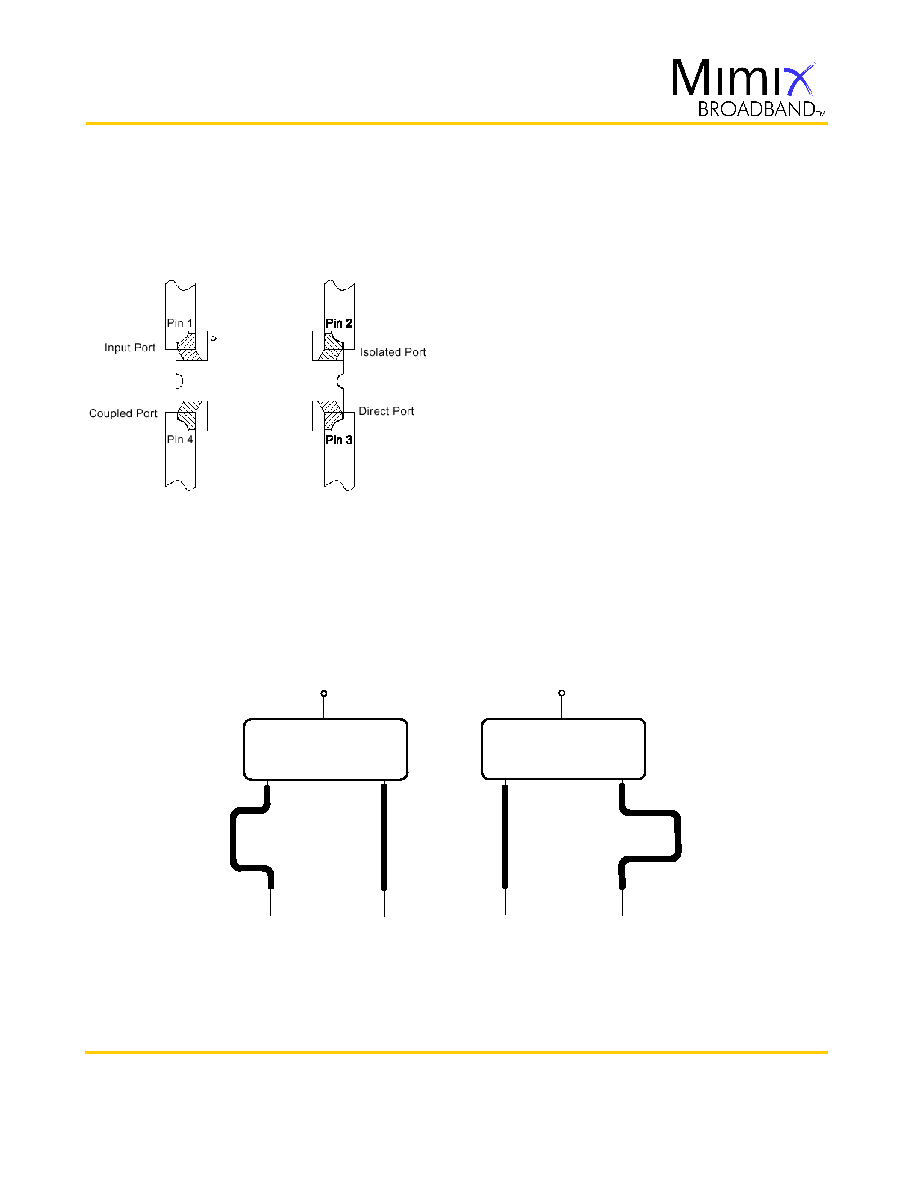
Mechanical Drawing
(Note: Engineering designator is 18KWR0327)
Units: millimeters (inches) Bond pad dimensions are shown to center of bond pad.
Thickness: 0.110 +/- 0.010 (0.0043 +/- 0.0004), Backside is ground, Bond Pad/Backside Metallization: Gold
All Bond Pads are 0.100 x 0.100 (0.004 x 0.004).
Bond pad centers are approximately 0.109 (0.004) from the edge of the chip.
Dicing tolerance: +/- 0.005 (+/- 0.0002). Approximate weight: 3.25 mg.
Bond Pad #1 (RF)
Bond Pad #2 (IF1)
Bond Pad #3 (LO)
Bond Pad #4 (IF2)
RF Arrangement
Page 4 of 6
18KWR0327
13.0-25.0 GHz GaAs MMIC
Image Reject Mixer
November 2005 - Rev 21-Nov-05
Pre-production
Mimix Broadband, Inc., 10795 Rockley Rd., Houston, Texas 77099
Tel: 281.988.4600 Fax: 281.988.4615 mimixbroadband.com
Characteristic Data and Specifications are subject to change without notice.
©
2005 Mimix Broadband, Inc.
Export of this item may require appropriate export licensing from the U.S. Government. In purchasing these parts, U.S. Domestic customers accept
their obligation to be compliant with U.S. Export Laws.
Page 5 of 6
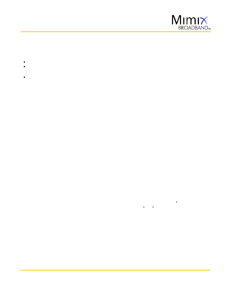
App Note [1] USB/LSB Selection
-
USB
LSB
IF1
IF2
An alternate method of Selection of USB or LSB:
13.0-25.0 GHz GaAs MMIC
Image Reject Mixer
18KWR0327
For Lower Side Band operation (LSB):
With IF1 and IF2 connected to the
direct port (0∫) and coupled port (90∫)
respectively as shown in the diagram,
the LSB signal will reside on the input
port. The isolated port must be loaded
with 50 ohms.
With IF1 and IF2 connected to the
direct port (0∫) and coupled port (90∫)
respectively as shown in the diagram,
the USB signal will reside on the
isolated port. The input port must be
loaded with 50 ohms.
For Upper Side Band operation (USB):
-90
o
In Phase Combiner
USB
In Phase Combiner
LSB
-90
o
IF2
IF1
IF2
IF1
November 2005 - Rev 21-Nov-05
Pre-production
Mimix Broadband, Inc., 10795 Rockley Rd., Houston, Texas 77099
Tel: 281.988.4600 Fax: 281.988.4615 mimixbroadband.com
Characteristic Data and Specifications are subject to change without notice.
©
2005 Mimix Broadband, Inc.
Export of this item may require appropriate export licensing from the U.S. Government. In purchasing these parts, U.S. Domestic customers accept
their obligation to be compliant with U.S. Export Laws.
Page 6 of 6
Handling and Assembly Information
CAUTION! - Mimix Broadband MMIC Products contain gallium arsenide (GaAs) which can be hazardous to the
human body and the environment. For safety, observe the following procedures:
Do not ingest.
Do not alter the form of this product into a gas, powder, or liquid through burning, crushing, or chemical
processing as these by-products are dangerous to the human body if inhaled, ingested, or swallowed.
Observe government laws and company regulations when discarding this product. This product must be
discarded in accordance with methods specified by applicable hazardous waste procedures.
Life Support Policy - Mimix Broadband's products are not authorized for use as critical components in life support
devices or systems without the express written approval of the President and General Counsel of Mimix
Broadband. As used herein: (1) Life support devices or systems are devices or systems which, (a) are intended for
surgical implant into the body, or (b) support or sustain life, and whose failure to perform when properly used in
accordance with instructions for use provided in the labeling, can be reasonably expected to result in a
significant injury to the user. (2) A critical component is any component of a life support device or system whose
failure to perform can be reasonably expected to cause the failure of the life support device or system, or to
affect its safety or effectiveness.
ESD - Gallium Arsenide (GaAs) devices are susceptible to electrostatic and mechanical damage. Die are supplied
in antistatic containers, which should be opened in cleanroom conditions at an appropriately grounded anti-
static workstation. Devices need careful handling using correctly designed collets, vacuum pickups or, with care,
sharp tweezers.
Die Attachment - GaAs Products from Mimix Broadband are 0.100 mm (0.004") thick and have vias through to the
backside to enable grounding to the circuit. Microstrip substrates should be brought as close to the die as
possible. The mounting surface should be clean and flat. If using conductive epoxy, recommended epoxies are
Ablestick 84-1LMI or 84-1LMIT cured in a nitrogen atmosphere per manufacturer's cure schedule. Apply epoxy
sparingly to avoid getting any on to the top surface of the die. An epoxy fillet should be visible around the total
die periphery. If eutectic mounting is preferred, then a fluxless gold-tin (AuSn) preform, approximately 0.001
thick, placed between the die and the attachment surface should be used. A die bonder that utilizes a heated
collet and provides scrubbing action to ensure total wetting to prevent void formation in a nitrogen atmosphere
is recommended. The gold-tin eutectic (80% Au 20% Sn) has a melting point of approximately 280 C (Note: Gold
Germanium should be avoided). The work station temperature should be 310 C 10 C. Exposure to these
extreme temperatures should be kept to minimum. The collet should be heated, and the die pre-heated to avoid
excessive thermal shock. Avoidance of air bridges and force impact are critical during placement.
Wire Bonding - Windows in the surface passivation above the bond pads are provided to allow wire bonding to
the die's gold bond pads. The recommended wire bonding procedure uses 0.076 mm x 0.013 mm (0.003" x
0.0005") 99.99% pure gold ribbon with 0.5-2% elongation to minimize RF port bond inductance. Gold 0.025 mm
(0.001") diameter wedge or ball bonds are acceptable for DC Bias connections. Aluminum wire should be
avoided. Thermo-compression bonding is recommended though thermosonic bonding may be used providing
the ultrasonic content of the bond is minimized. Bond force, time and ultrasonics are all critical parameters.
Bonds should be made from the bond pads on the die to the package or substrate. All bonds should be as short
as possible.
2
+
-
18KWR0327
13.0-25.0 GHz GaAs MMIC
Image Reject Mixer
November 2005 - Rev 21-Nov-05