 | –≠–ª–µ–∫—Ç—Ä–æ–Ω–Ω—ã–π –∫–æ–º–ø–æ–Ω–µ–Ω—Ç: 20DBL0451 | –°–∫–∞—á–∞—Ç—å:  PDF PDF  ZIP ZIP |

Pre-production
Mimix Broadband
'
s two stage 10.0-13.0/20.0-26.0 GHz
GaAs MMIC doubler has a +15.0 dBm output drive
and is an excellent LO doubler that can be used to
drive fundamental mixer devices. It is also well suited
to drive Mimix's XR1002 receiver device. This MMIC
uses Mimix Broadband
'
s 0.15
µ
m GaAs PHEMT device
model technology, and is based upon electron beam
lithography to ensure high repeatability and
uniformity. The chip has surface passivation to protect
and provide a rugged part with backside via holes
and gold metallization to allow either a conductive
epoxy or eutectic solder die attach process. This
device is well suited for Millimeter-wave Point-to-
Point Radio, LMDS, SATCOM and VSAT applications.
10.0-13.0/20.0-26.0 GHz GaAs MMIC
Active Doubler
Excellent Mixer Driver
2-Stage Active Design
Can be Used to Drive XR1002 Receiver
+15 dBm Output Drive
100% On-Wafer RF, DC and Output Power Testing
100% Visual Inspection to MIL-STD-883
Method 2010
Features
General Description
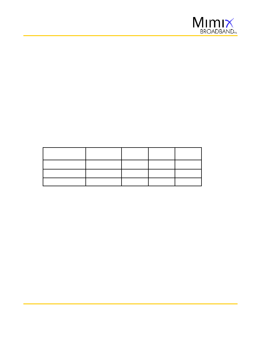
Electrical Characteristics (Ambient Temperature T = 25
o
C)
Parameter
Input Frequency Range (fin)
Output Frequency Range (fout)
Input Return Loss (S11)
Output Return Loss (S22)
Fundamental Level at the Output
RF Input Power (RF Pin)
Output Power at +9.0 dBm Pin (Pout)
Drain Bias Voltage (Vd1,2)
Gate Bias Voltage (Vg1)
Gate Bias Voltage (Vg2)
Supply Current
(Id1,2) (Vd=3.5V, Vg1=-0.7V, Vg2=-0.2 Typical)
Units
GHz
GHz
dB
dB
dBc
dBm
dBm
VDC
VDC
VDC
mA
Min.
10.0
20.0
-
-
-
-
-
-
-1.2
-1.2
-
Typ.
-
-
TBD
TBD
-30.0
+9.0
+15.0
+3.5
-0.7
-0.2
70
Max.
13.0
26.0
-
-
-
-
-
+5.5
+0.1
+0.1
100
Absolute Maximum Ratings
Supply Voltage (Vd)
Supply Current (Id)
Gate Bias Voltage (Vg)
Input Power (RF Pin)
Storage Temperature (Tstg)
Operating Temperature (Ta)
Channel Temperature (Tch)
+6.0 VDC
110 mA
+0.3 VDC
+15.0 dBm
-65 to +165
O
C
-55 to MTTF Table
MTTF Table
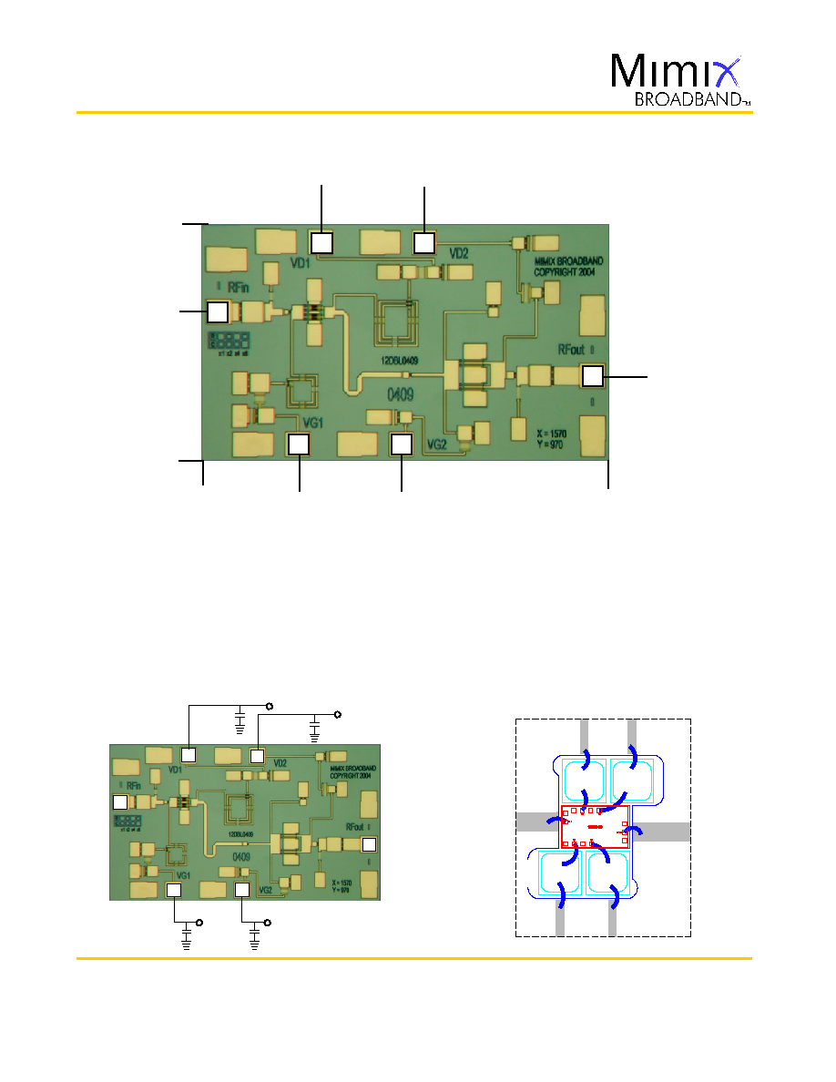
Chip Device Layout
12DBL0409
Page 1 of 6
1
(1) Channel temperature affects a device's MTBF. It is
recommended to keep channel temperature as low as
possible for maximum life.
1
Mimix Broadband, Inc., 10795 Rockley Rd., Houston, Texas 77099
Tel: 281.988.4600 Fax: 281.988.4615 mimixbroadband.com
Characteristic Data and Specifications are subject to change without notice.
©
2005 Mimix Broadband, Inc.
Export of this item may require appropriate export licensing from the U.S. Government. In purchasing these parts, U.S. Domestic customers accept
their obligation to be compliant with U.S. Export Laws.
March 2005 - Rev 01-Mar-05

Pre-production
10.0-13.0/20.0-26.0 GHz GaAs MMIC
Active Doubler
Doubler Measurements
12DBL0409
Page 2 of 6
Mimix Broadband, Inc., 10795 Rockley Rd., Houston, Texas 77099
Tel: 281.988.4600 Fax: 281.988.4615 mimixbroadband.com
Characteristic Data and Specifications are subject to change without notice.
©
2005 Mimix Broadband, Inc.
Export of this item may require appropriate export licensing from the U.S. Government. In purchasing these parts, U.S. Domestic customers accept
their obligation to be compliant with U.S. Export Laws.
March 2005 - Rev 01-Mar-05
0409_typical: Pout (2xFin) vs. Fin (GHz)
Pin = 6 & 9dBm, Regulated Bias: VD1=3.5V, ID1=20mA, VD2=3.5, ID2=50mA
-30
-25
-20
-15
-10
-5
0
5
10
15
20
6
7
8
9
10
11
12
13
14
15
16
Fin (GHz)
P
o
ut
(
2
xF
i
n
)
, Pin (dBm)=6
, Pin (dBm)=9
, Pin (dBm)=6
, Pin (dBm)=9
Pout (2xFin)
Pout (1xFin)
0409_wafer_sweep: Pout (2xFin) vs. Fin (GHz)
Pin = 9dBm, Regulated Bias: VD1=3.5V, ID1=20mA, VD2=3.5, ID2=50mA
0
2
4
6
8
10
12
14
16
18
20
8
9
10
11
12
13
14
15
Fin (GHz)
P
o
u
t
(
2
x
F
in
)
Pout (2xFin)
0409_wafer_sweep: Pout (2xFin) vs. Fin (GHz)
Pin = 9dBm, Regulated Bias: VD1=3.5V, ID1=20mA, VD2=3.5, ID2=50mA
-30
-25
-20
-15
-10
-5
0
5
10
15
20
8
9
10
11
12
13
14
15
Fin (GHz)
P
out
(
2
xF
i
n
)
Pout (2xFin)
Pout (1xFin)
RF In
RF Out
1
2
3
4
5
6
Vd1
Vd2
Vg1
Vg2
0.970
(0.038)
1
2
3
4
5
6
0.483
(0.019)
0.881
(0.035)
0.362
(0.014)
0.795
(0.031)
1.620
(0.064)
0.394
(0.016)
0.0
0.0
0.605
(0.024)
Pre-production
10.0-13.0/20.0-26.0 GHz GaAs MMIC
Active Doubler
Mechanical Drawing
12DBL0409
Page 3 of 6
Mimix Broadband, Inc., 10795 Rockley Rd., Houston, Texas 77099
Tel: 281.988.4600 Fax: 281.988.4615 mimixbroadband.com
Characteristic Data and Specifications are subject to change without notice.
©
2005 Mimix Broadband, Inc.
Export of this item may require appropriate export licensing from the U.S. Government. In purchasing these parts, U.S. Domestic customers accept
their obligation to be compliant with U.S. Export Laws.
March 2005 - Rev 01-Mar-05
Bias Arrangement
Bypass Capacitors - See App Note [2]
(Note: Engineering designator is 12DBL0409)
Units: millimeters (inches) Bond pad dimensions are shown to center of bond pad.
Thickness: 0.115 +/- 0.010 (0.0045 +/- 0.0004), Backside is ground, Bond Pad/Backside Metallization: Gold
All Bond Pads are 0.100 x 0.100 (0.004 x 0.004).
Bond pad centers are approximately 0.109 (0.004) from the edge of the chip.
Dicing tolerance: +/- 0.005 (+/- 0.0002). Approximate weight: 0.974 mg.
Bond Pad #1 (RF In)
Bond Pad #2 (Vd1)
Bond Pad #3 (Vd2)
Bond Pad #4 (RF Out)
Bond Pad #5 (Vg2)
Bond Pad #6 (Vg1)
RF In
Vd1
Vd2
RF Out
Vg2
Vg1
Pre-production
10.0-13.0/20.0-26.0 GHz GaAs MMIC
Active Doubler
12DBL0409
Page 4 of 6
Mimix Broadband, Inc., 10795 Rockley Rd., Houston, Texas 77099
Tel: 281.988.4600 Fax: 281.988.4615 mimixbroadband.com
Characteristic Data and Specifications are subject to change without notice.
©
2005 Mimix Broadband, Inc.
Export of this item may require appropriate export licensing from the U.S. Government. In purchasing these parts, U.S. Domestic customers accept
their obligation to be compliant with U.S. Export Laws.
March 2005 - Rev 01-Mar-05
App Note [1] Biasing
-
It is recommended to separately bias each doubler stage Vd1 through Vd2 at Vd(1,2)=3.5V with Id1=20mA
and Id2=50mA. Separate biasing is recommended if the doubler is to be used at high levels of saturation, where gate rectification
will alter the effective gate control voltage. It is also recommended to use active biasing to keep the currents constant as the RF
power and temperature vary; this gives the most reproducible results. Depending on the supply voltage available and the power
dissipation constraints, the bias circuit may be a single transistor or a low power operational amplifier, with a low value resistor in
series with the drain supply used to sense the current. The gate of the pHEMT is controlled to maintain correct drain current and
thus drain voltage. The typical gate voltages needed to do this are Vg1=-0.7V and Vg2=-0.2V. Typically the gate is protected with
Silicon diodes to limit the applied voltage. Also, make sure to sequence the applied voltage to ensure negative gate bias is available
before applying the positive drain supply.
App Note [2] Bias Arrangement
-
For individual Stage Bias (Recommended for doubler applications) -- Each DC pad (Vd1, 2 and Vg1, 2) needs to have DC bypass
capacitance (~100-200 pf ) as close to the device as possible. Additional DC bypass capacitance (~0.01 uF) is also recommended.
MTTF Tables
Backplate
Temperature
55 deg Celsius
75 deg Celsius
95 deg Celsius
Channel
Temperature
96.6 deg Celsius
119.6 deg Celsius
142.3 deg Celsius
FITs
3.64E-02
5.13E-01
5.24E+00
MTTF Hours
2.75E+10
1.95E+09
1.91E+08
Rth
169.6
∞
C/W
181.9
∞
C/W
193.0
∞
C/W
Bias Conditions: Vd1=Vd2=3.5V, Id1=20 mA, Id2=50 mA
These numbers were calculated based on accelerated life test information and thermal model analysis received from the fabricating foundry.
Pre-production
10.0-13.0/20.0-26.0 GHz GaAs MMIC
Active Doubler
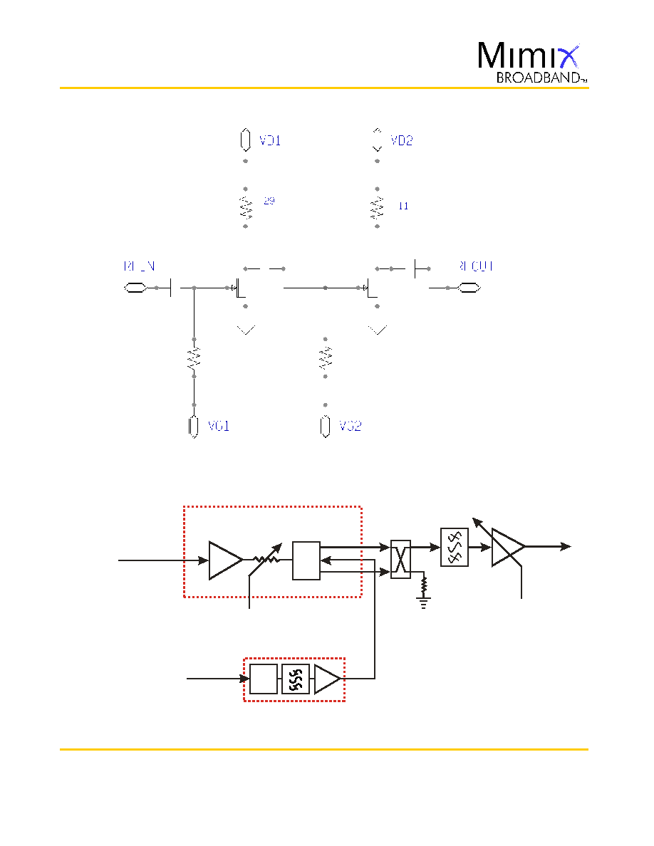
Device Schematic
12DBL0409
Page 5 of 6
Mimix Broadband, Inc., 10795 Rockley Rd., Houston, Texas 77099
Tel: 281.988.4600 Fax: 281.988.4615 mimixbroadband.com
Characteristic Data and Specifications are subject to change without notice.
©
2005 Mimix Broadband, Inc.
Export of this item may require appropriate export licensing from the U.S. Government. In purchasing these parts, U.S. Domestic customers accept
their obligation to be compliant with U.S. Export Laws.
March 2005 - Rev 01-Mar-05
Typical Application
RF IN
21.5-23.5 GHz
IR Mixer
XR1002
BPF
IF Out
2 GHz
Atten=0-12dB
AGC Control
LO(+9.0dBm)
9.75-11.75 GHz
11.75-12.75 GHz
19.5-21.5 GHz (USB Operation)
23.5-25.5 GHz (LSB Operation)
12DBL0409
Mimix
Broadband MMIC-based 20.0-26.0 GHz Doubler/Receiver Block Diagram
(Changing LO and IF frequencies as required allows design to operate as high as 26 GHz)
X2