 | –≠–ª–µ–∫—Ç—Ä–æ–Ω–Ω—ã–π –∫–æ–º–ø–æ–Ω–µ–Ω—Ç: 7OSC0462 | –°–∫–∞—á–∞—Ç—å:  PDF PDF  ZIP ZIP |

Pre-production
Mimix Broadband, Inc., 10795 Rockley Rd., Houston, Texas 77099
Tel: 281.988.4600 Fax: 281.988.4615 mimixbroadband.com
Characteristic Data and Specifications are subject to change without notice.
©
2005 Mimix Broadband, Inc.
Export of this item may require appropriate export licensing from the U.S. Government. In purchasing these parts, U.S. Domestic customers accept
their obligation to be compliant with U.S. Export Laws.
May 2005 - Rev 05-May-05
Units
GHz
dBm
dBc/Hz
dBc/Hz
dBc
dBc
dBc
MHz/Volt
VDC
VDC
mA
Min.
6.4
-
-
-
-
-
-
-
-
+0.0
-
Typ.
-
+5.0
-97.0
-118.0
-17.0
-27.0
-37.0
60.0
-5.0
-
20
Max.
7.4
-
-
-
-
-
-
-
-
+6.0
25
6.4-7.4 GHz GaAs MMIC
Voltage Controlled Oscillator
Page 1 of 5
Features
On-Chip Resonator
+5.0 dBm Output Power
-97 dBc/Hz @ 100KHz Phase Noise
20mA @ -5.0V Bias Supply
100% On-Wafer, DC and Output Power Testing
100% Visual Inspection to MIL-STD-883
Method 2010
General Description
Parameter
Supply Voltage (Vee1,2,3)
Supply Voltage (Vtune)
Supply Current (Iee1,2,3)
Supply Current (Itune)
Storage Temperature (Tstg)
Operating Temperature (Ta)
Junction Temperature (Tjn)
-6.0 VDC
+6.0 VDC
30 mA
1 mA
-65 to +165
O
C
-55 to MTTF Table
MTTF Table
Chip Device Layout
(1) Junction temperature affects a device's MTTF. It is
recommended to keep channel temperature as low as
possible for maximum life.
1
1
Mimix Broadband's 6.4-7.4 GHz GaAs HBT VCO is a fully
integrated oscillator MMIC with on-chip tuning diode and
resonator. This design is based on a cross coupled differential
pair with on-chip buffer amplifier and output balun. The use of
a high-Q resonator structure and integrated varactor diodes
results in optimum phase-noise performance. This MMIC uses
Mimix Broadband's 2 um GaAs HBT device model technology
to ensure low flicker (1/f ) noise and high reliability. The chip
has surface passivation to protect and provide a rugged part
with backside via holes and gold metallization to allow either a
conductive epoxy or eutectic solder die attach process. This
device is well suited for Millimeter-wave Point-to-Point Radio,
LMDS, SATCOM and VSAT applications.
Electrical Characteristics (Ambient Temperature T = 25
o
C)
Absolute Maximum Ratings
Frequency Range (f )
Fundamental Output Power (Pout)
SSB Phase Noise @ 100 kHz Offset
SSB Phase Noise @ 1 MHz Offset
2nd Harmonic Suppression
3rd Harmonic Suppression
4th Harmonic Suppression
Frequency Pushing (Vee)
Supply Voltage (Vee)
Frequency Tuning Voltage (Vtune)
Supply Current (Iee) (Vee=-5.0V Typical)
7OSC0462
Pre-production
Mimix Broadband, Inc., 10795 Rockley Rd., Houston, Texas 77099
Tel: 281.988.4600 Fax: 281.988.4615 mimixbroadband.com
Characteristic Data and Specifications are subject to change without notice.
©
2005 Mimix Broadband, Inc.
Export of this item may require appropriate export licensing from the U.S. Government. In purchasing these parts, U.S. Domestic customers accept
their obligation to be compliant with U.S. Export Laws.
Page 2 of 5
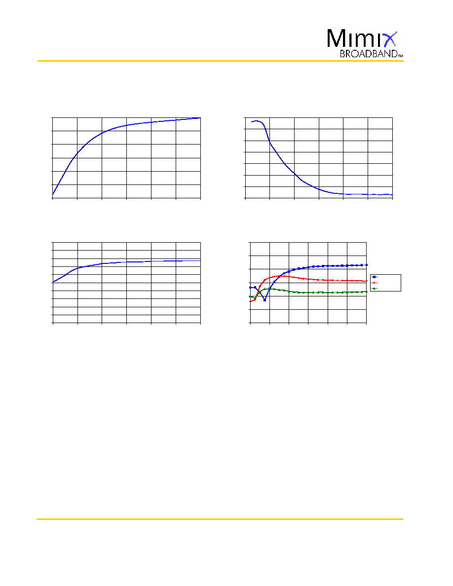
Oscillator Measurements
May 2005 - Rev 05-May-05
6.4-7.4 GHz GaAs MMIC
Voltage Controlled Oscillator
7OSC0462
7OSC0462 Output Frequency vs. Tuning Voltage
6.2
6.4
6.6
6.8
7
7.2
7.4
0
1
2
3
4
5
6
Vtune (Volts)
Fout (GHz
)
7OSC0462 Kvco vs. Tuning Voltage
0
100
200
300
400
500
600
700
0
1
2
3
4
5
6
Vtune (Volts)
Kvco (MHz/Volt)
7OSC0462 Output Power vs. Tuning Voltage
-10
-8
-6
-4
-2
0
2
4
6
8
10
0
1
2
3
4
5
6
Vtune (Volts)
P
o
ut (dBm)
7OSC0462 Harmonic Levels vs. Tuning Voltage
-60
-50
-40
-30
-20
-10
0
0
1
2
3
4
5
6
Vtune (Volts)
Pharm (dBc)
Pharm_2nd
Pharm_3rd
Pharm_4th
1
3
2
4
5
6
Vee2
Vee3
RF Out
Vee1
Vtune
(Maximum 100pF)
1
3
1.800
(0.071)
1.105
(0.044)
2
1.504
(0.060)
0.0
0.0
1.504
(0.060)
4
1.105
(0.044)
5
0.566
(0.022)
0.673
(0.027)
1.350
(0.053)
6
Pre-production
Mimix Broadband, Inc., 10795 Rockley Rd., Houston, Texas 77099
Tel: 281.988.4600 Fax: 281.988.4615 mimixbroadband.com
Characteristic Data and Specifications are subject to change without notice.
©
2005 Mimix Broadband, Inc.
Export of this item may require appropriate export licensing from the U.S. Government. In purchasing these parts, U.S. Domestic customers accept
their obligation to be compliant with U.S. Export Laws.
Page 3 of 5
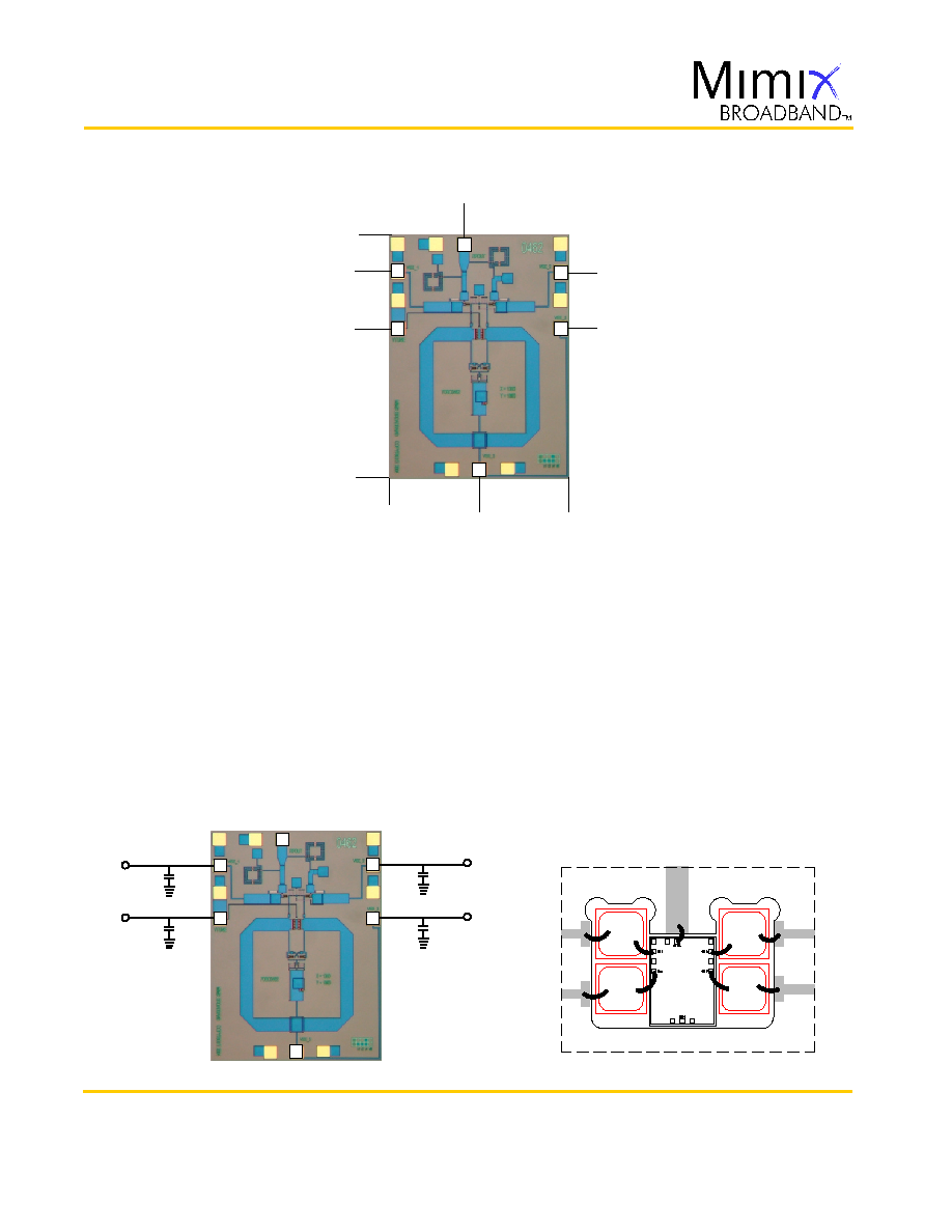
Mechanical Drawing
Bias Arrangement
Bypass Capacitors
- See App Note [2]
(Note: Engineering designator is 7OSC0462)
Units: millimeters (inches) Bond pad dimensions are shown to center of bond pad.
Thickness: 0.110 +/- 0.010 (0.0043 +/- 0.0004), Backside is ground, Bond Pad/Backside Metallization: Gold
All Bond Pads are 0.100 x 0.100 (0.004 x 0.004).
Bond pad centers are approximately 0.109 (0.004) from the edge of the chip.
Dicing tolerance: +/- 0.005 (+/- 0.0002). Approximate weight: 1.507 mg.
Bond Pad #1 (Vtune)
Bond Pad #2 (Vee1)
Bond Pad #3 (RF Out)
Bond Pad #4 (Vee2)
Bond Pad #5 (Vee3)
Bond Pad #6 (Vee3)
May 2005 - Rev 05-May-05
6.4-7.4 GHz GaAs MMIC
Voltage Controlled Oscillator
7OSC0462
7OSC0462
Vee1
Vtune
RF Out
Vee2
Vee3
Pre-production
Mimix Broadband, Inc., 10795 Rockley Rd., Houston, Texas 77099
Tel: 281.988.4600 Fax: 281.988.4615 mimixbroadband.com
Characteristic Data and Specifications are subject to change without notice.
©
2005 Mimix Broadband, Inc.
Export of this item may require appropriate export licensing from the U.S. Government. In purchasing these parts, U.S. Domestic customers accept
their obligation to be compliant with U.S. Export Laws.
Page 4 of 5
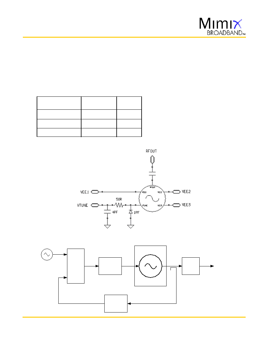
App Note [1] Biasing
- As shown in the bonding diagram, this device is operated by separately biasing Vee1, Vee2, Vee3 and Vtune with
Vee1 = Vee2 = Vee3 = -5.0 V and Vtune = 0.0 to 6.0 V, Iee1 = Iee2 = Iee3 = ~ 6.5 mA.
App Note [2] Bias Arrangement
- Each DC pad (Vee1, 2, 3 and Vtune) needs to have DC bypass capacitance. (~100 - 200 pF, 100pF max on
Vtune) as close to the device as possible. The Vee3 pads have been tied together on chip and can be biased from either location.
Functional Diagram & Vtune Equivalent Input Circuit
Typical Application
MTTF Table
Backplate
Temperature
55 deg Celsius
75 deg Celsius
95 deg Celsius
FITs
2.00E-01
2.88E+00
3.02E+01
MTTF Hours
4.99E+09
3.47E+08
3.31E+07
These numbers were calculated based on accelerated life test information and thermal model analysis received from the fabricating foundry.
May 2005 - Rev 05-May-05
6.4-7.4 GHz GaAs MMIC
Voltage Controlled Oscillator
7OSC0462
Prescalar
Doubler
PLL IC
7OSC0462
Ref 10 MHz
Loop
Filter
Icp
Vtune
Fvco
Fout
Fsample
6.4 - 7.4 GHz
12.8-14.8 GHz

Pre-production
Mimix Broadband, Inc., 10795 Rockley Rd., Houston, Texas 77099
Tel: 281.988.4600 Fax: 281.988.4615 mimixbroadband.com
Characteristic Data and Specifications are subject to change without notice.
©
2005 Mimix Broadband, Inc.
Export of this item may require appropriate export licensing from the U.S. Government. In purchasing these parts, U.S. Domestic customers accept
their obligation to be compliant with U.S. Export Laws.
Page 5 of 5
Handling and Assembly Information
CAUTION! - Mimix Broadband MMIC Products contain gallium arsenide (GaAs) which can be hazardous to the
human body and the environment. For safety, observe the following procedures:
Do not ingest.
Do not alter the form of this product into a gas, powder, or liquid through burning, crushing, or chemical
processing as these by-products are dangerous to the human body if inhaled, ingested, or swallowed.
Observe government laws and company regulations when discarding this product. This product must be
discarded in accordance with methods specified by applicable hazardous waste procedures.
Life Support Policy - Mimix Broadband's products are not authorized for use as critical components in life support
devices or systems without the express written approval of the President and General Counsel of Mimix
Broadband. As used herein: (1) Life support devices or systems are devices or systems which, (a) are intended for
surgical implant into the body, or (b) support or sustain life, and whose failure to perform when properly used in
accordance with instructions for use provided in the labeling, can be reasonably expected to result in a
significant injury to the user. (2) A critical component is any component of a life support device or system whose
failure to perform can be reasonably expected to cause the failure of the life support device or system, or to
affect its safety or effectiveness.
ESD - Gallium Arsenide (GaAs) devices are susceptible to electrostatic and mechanical damage. Die are supplied
in antistatic containers, which should be opened in cleanroom conditions at an appropriately grounded anti-
static workstation. Devices need careful handling using correctly designed collets, vacuum pickups or, with care,
sharp tweezers.
Die Attachment - GaAs Products from Mimix Broadband are 0.100 mm (0.004") thick and have vias through to the
backside to enable grounding to the circuit. Microstrip substrates should be brought as close to the die as
possible. The mounting surface should be clean and flat. If using conductive epoxy, recommended epoxies are
Ablestick 84-1LMI or 84-1LMIT cured in a nitrogen atmosphere per manufacturer's cure schedule. Apply epoxy
sparingly to avoid getting any on to the top surface of the die. An epoxy fillet should be visible around the total
die periphery. If eutectic mounting is preferred, then a fluxless gold-tin (AuSn) preform, approximately 0.001
thick, placed between the die and the attachment surface should be used. A die bonder that utilizes a heated
collet and provides scrubbing action to ensure total wetting to prevent void formation in a nitrogen atmosphere
is recommended. The gold-tin eutectic (80% Au 20% Sn) has a melting point of approximately 280 C (Note: Gold
Germanium should be avoided). The work station temperature should be 310 C 10 C. Exposure to these
extreme temperatures should be kept to minimum. The collet should be heated, and the die pre-heated to avoid
excessive thermal shock. Avoidance of air bridges and force impact are critical during placement.
Wire Bonding - Windows in the surface passivation above the bond pads are provided to allow wire bonding to
the die's gold bond pads. The recommended wire bonding procedure uses 0.076 mm x 0.013 mm (0.003" x
0.0005") 99.99% pure gold ribbon with 0.5-2% elongation to minimize RF port bond inductance. Gold 0.025 mm
(0.001") diameter wedge or ball bonds are acceptable for DC Bias connections. Aluminum wire should be
avoided. Thermo-compression bonding is recommended though thermosonic bonding may be used providing
the ultrasonic content of the bond is minimized. Bond force, time and ultrasonics are all critical parameters.
Bonds should be made from the bond pads on the die to the package or substrate. All bonds should be as short
as possible.
2
+
-
May 2005 - Rev 05-May-05
6.4-7.4 GHz GaAs MMIC
Voltage Controlled Oscillator
7OSC0462