3236 Scott Boulevard
Santa Clara, California 95054
Phone: (408) 986-5060
Fax: (408) 986-5095
CFK2162-P5
Features
t High Gain
t +34 dBm Power Output
t Proprietary Power FET Process
t >45% Linear Power Added Efficiency
t +29 dBm with 30 dBc Third Order Products
t Surface Mount SO-8 Power Package
Applications
t ISM Band Base Stations and Terminals
t PCS/PCN Base Stations and Terminals
t Wireless Local Loop
Description
The CFK2162-P5 is a high-gain FET intended for dri-
ver amplifier applications in high-power systems, and output
stage usage in medium power applications at power levels up to
+34 dBm. The device is easily matched and provides excellent
linearity at 2 Watts. Manufactured in Celeritek's proprietary
power FET process, this device is assembled in an industry
standard surface mount SO-8 power package that is compatible
with high volume, automated board assembly techniques.
2.3 to 2.5 GHz
+34 dBm Power GaAs FET
Product Specifications
July 1997
(1 of 4)
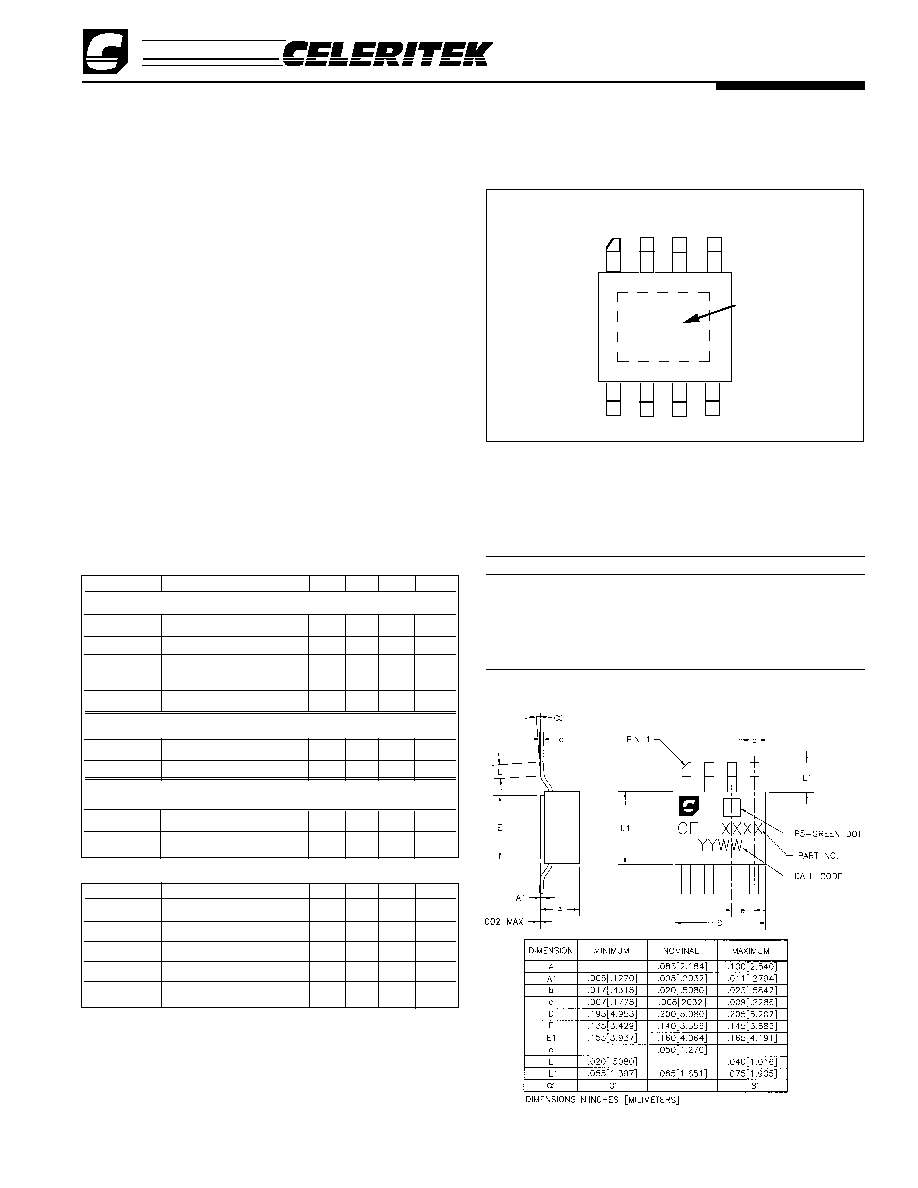
1
3
4
7
8
6
5
2
G
G
D
D
Back Plane
is Source
GND
GND
GND
GND
Package Diagram
Notes:
1. Sum to two tones with 1 MHz spacing = 29 dBm.
2. See thermal considerations information on page 4.
3. Max (+Vd) and (-Vg) under linear operation. Max potential difference
across the device in RF compression (2Vd + |-Vg|) not to exceed the mini-
mum breakdown voltage (Vbr) of +18V.
Absolute Maximum Ratings
Parameter
Symbol
Rating
Drain-Source Voltage
VDS
12V (3)
Gate-Source Voltage
VGS
-5V
Drain Current
IDS
Idss
Continuous Dissipation
PT
10W
Channel Temperature
TCH
175∞C
Storage Temperature
TSTG
-65∞C to +175∞C
Parameters
Conditions
Min
Typ
Max
Units
Vd = 8V, Id = 800 mA (Quiescent)
P-1dB
33.0 34.0
--
dBm
SSG
11.0 12.0
--
dB
3rd Order
Products (1)
26
30
--
dBc
Efficiency
@ P1dB
--
40
--
%
Vd = 5V, Id = 350 mA (Quiescent)
P-1dB
--
30.0
--
dBm
SSG
--
9.0
--
dB
Vd = 5V, Id = 1200 mA (Quiescent)
P-1dB
--
32.5
--
dBm
SSG
--
10.0
--
dB
Specifications
(TA = 25∞C)
The following specifications are
guaranteed at room temperature in Celeritek test fixture at 2.5 GHz.
Parameters
Conditions
Min
Typ
Max
Units
gm
Vds = 2.0V, Vgs = 0V
--
1700
--
mS
Idss
Vds = 2.0V, Vgs = 0V
--
2.8
--
A
Vp
Vds = 3.0V, Ids = 65 mA
--
-1.8
Volts
BVGD (3)
Igd = 6.5 mA
18
20
--
Volts
JL (2)
@150∞C TCH
--
10
--
∞C/W
SO-8 Power Package Physical Dimensions
3236 Scott Boulevard, Santa Clara, California 95054
Phone: (408) 986-5060
Fax: (408) 986-5095
CFK2162-P5
Product Specifications - July 1997
(2 of 4)
RF Match Data shown in the performance graphs was taken
in the test circuits shown at right and on page 3. Layout is
important for proper operation. Phase length of input and out-
put 50
line varies as a function of exact desired frequency
of operation. Output shunt inductor effects output perfor-
mance. Celeritek recommends the use of a high impedance
printed inductor Lambda/4 in length. Please contact the facto-
ry for an evaluation board and/or more detailed application
support.
Typical Scattering Parameters
(TA = 25∞C, Vds = 5 V, Ids = 350 mA)
Frequency
S11
S21
S12
S22
(GHz)
Mag
Ang
Mag
Ang
Mag
Ang
Mag
Ang
0.6
0.946
-162.45
4.973
86.73
0.017
11.14
0.739
172.95
1.0
0.946
-176.06
2.885
73.75
0.018
9.37
0.748
169.73
1.8
0.927
172.61
1.873
54.47
0.023
1.6
0.707
161.84
1.9
0.922
169.71
1.828
50.82
0.023
-0.79
0.70
158.98
1.5
0.938
178.31
2.055
63.25
0.02
4.93
0.73
167.15
2.0
0.918
166.09
1.777
46.63
0.025
-1.23
0.694
155.54
2.1
0.914
161.9
1.722
42.23
0.024
-4.64
0.69
151.93
2.2
0.912
157.79
1.664
37.59
0.026
-9.26
0.689
148.15
2.3
0.914
153.46
1.578
34.07
0.023
-17.03
0.703
143.83
2.4
0.914
148.95
1.503
29.83
0.023
-21.0
0.707
139.91
2.5
0.918
145.37
1.431
26.13
0.023
-22.87
0.714
137.02
2.6
0.921
141.59
1.344
22.16
0.022
-28.45
0.722
134.0
2.7
0.923
138.23
1.254
18.61
0.022
-28.3
0.735
131.62
3.0
0.941
132.34
1.033
10.11
0.022
-27.73
0.76
128.69
3.5
0.957
134.66
0.803
6.12
0.02
-21.78
0.787
132.92
4.0
0.94
138.76
0.803
1.66
0.023
-20.57
0.74
136.51
(TA = 25∞C, Vds = 5 V, Ids = 1200 mA)
0.6
0.95
-165
5.311
84.94
0.014
13.61
0.747
17.19
1.0
0.951
-177.94
3.044
72.23
0.014
14.39
0.749
168.92
1.8
0.935
171.39
1.98
53.44
0.018
10.27
0.703
161.07
1.9
0.931
168.6
1.93
49.72
0.019
5.75
0.696
158.27
2.0
0.929
165.15
1.88
45.76
0.02
7.43
0.69
154.9
2.1
0.925
161.29
1.822
41.44
0.02
4.37
0.686
151.32
2.2
0.924
157.02
1.757
36.86
0.021
2.36
0.687
147.44
2.3
0.92
152.84
1.765
32.59
0.02
-5.07
0.679
144.99
2.4
0.923
148.35
1.673
28.03
0.021
-71.14
0.684
141.21
2.5
0.923
144.9
1.603
24.44
0.021
-9.31
0.692
138.25
2.6
0.927
141.0
1.503
20.51
0.02
-11.55
0.702
135.31
2.7
0.93
137.72
1.406
16.94
0.02
-14.27
0.711
132.91
3.0
0.947
131.72
1.09
9.25
0.018
-17.77
0.757
127.79
3.5
0.961
133.41
0.853
4.59
0.017
-13.03
0.779
131.26
4.0
0.945
137.83
0.85
0.36
0.021
-8.72
0.73
134.73
(TA = 25∞C, Vds = 8 V, Ids = 800 mA)
0.6
0.941
-164.65
5.654
83.55
0.015
10.74
0.676
174.61
1.0
0.947
-177.32
3.25
70.11
0.015
8.2
0.688
171.96
1.8
0.93
171.59
2.058
49.6
0.018
6.89
0.652
165.68
1.9
0.927
168.63
2.006
45.54
0.019
3.81
0.644
163.07
2.0
0.923
165.04
1.99
41.52
0.019
-1.07
0.639
159.85
2.1
0.919
160.94
1.885
36.76
0.02
-1.68
0.635
156.23
2.2
0.917
156.65
1.714
32.35
0.02
-2.32
0.636
152.38
2.3
0.921
153.49
1.779
29.48
0.018
-14.97
0.642
148.42
2.4
0.921
149.12
1.688
24.79
0.018
-16.28
0.648
144.43
2.5
0.925
145.41
1.616
21.01
0.017
-20.8
0.656
141.59
2.6
0.927
141.65
1.518
16.92
0.017
-23.5
0.667
138.37
2.7
0.933
138.32
1.417
13.24
0.017
-25.79
0.681
136.05
3.0
0.944
131.73
1.116
3.58
0.018
-21.43
0.722
132.33
3.5
0.96
134.09
0.857
-1.39
0.016
-16.54
0.762
136.36
4.0
0.942
137.96
0.841
-6.32
0.02
-10.57
0.723
140.71
15 pF
1.8 pF
RF
OUT
RF
IN
CFK2162-P5, 5V, 350 mA
50
uuuu
Vg
uuuu
100 pF
50
0.1 µF
7.5
0.1 µF
91
100
pF
Vd
1.5 pF
1.5 pF
1.8 pF
47 nH
100 nH
3236 Scott Boulevard
Santa Clara, California 95054
Phone: (408) 986-5060
Fax: (408) 986-5095
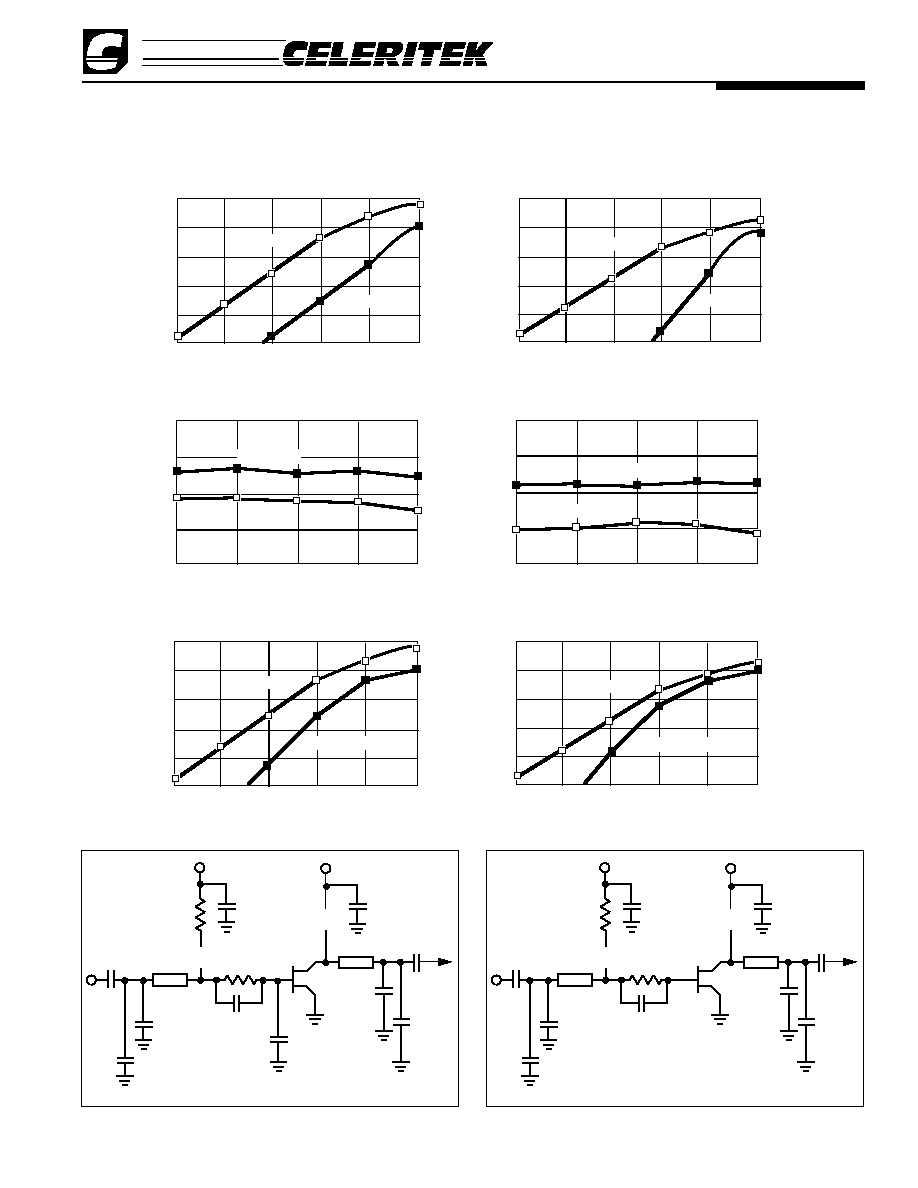
Power Output & Power Added Efficiency vs Power Input
2.45 GHz, VDS = 5 V, IDS = 1.2 A
Power Input (dBm)
Power Output (dBm)
Efficiency (%)
Efficiency
Power Output
0
10
20
30
40
50
10
15
20
25
30
35
1
6
11
21
26
16
Power Output & Power Added Efficiency vs Power Input
2.45 GHz, VDS = 8 V, IDS = 800 mA
Power Input (dBm)
Power Output (dBm)
Efficiency (%)
Efficiency
Power Output
0
10
20
30
40
50
10
15
20
25
30
35
0
5
10
20
25
15
Frequency, GHz
Power Output @ P
-1 dB
Gain @ P
-1 dB
Power Output
11
12
13
14
9
Gain
29
31
33
35
37
Power Output and Gain vs Frequency
VDS =5V, IDS = 1200 mA
2.3
2.4
2.5
2.25
2.45
Power Output & 3rd Order Products vs Power Input
2.45 GHz, VDS = 5 V, IDS = 1.2 A
Power Input (dBm)
Power Output (dBm)
3rd Order Products (dBc)
3rd Order Products
Power Output
55
45
35
25
15
5
10
15
20
25
30
35
1
6
11
21
26
16
Power Output & 3rd Order Products vs Power Input
2.45 GHz, VDS = 8 V, IDS = 800 mA
Power Input (dBm)
Power Output (dBm)
3rd Order Products (dBc)
3rd Order Products
Power Output
55
45
35
25
15
5
10
15
20
25
30
35
0
5
10
20
25
15
Frequency, GHz
Power Output and Gain vs Frequency
VDS =8V, IDS = 800 mA
Power Output @ P
-1 dB
Gain
11
12
13
14
10
29
31
33
35
37
Power Output
Gain @ P
-1 dB
2.3
2.4
2.5
2.25
2.45
CFK2162-P5
Product Specifications - July 1997
(3 of 4)
Typical Performance
15 pF
1.5 pF
RF
OUT
RF
IN
CFK2162-P5, 5V, 1200 mA
50
uuuu
Vg
uuuu
100 pF
50
0.1 µF
7.5
0.1 µF
91
100
pF
Vd
1.8 pF
1.5 pF
1.2 pF
1.8 pF
47 nH
100 nH
15 pF
1.5 pF
RF
OUT
RF
IN
CFK2162-P5, 8V, 800 mA
50
uuuu
Vg
uuuu
100 pF
50
0.1 µF
7.5
0.1 µF
91
100
pF
Vd
1.8 pF
0.6 pF
1.8 pF
47 nH
100 nH
3236 Scott Boulevard, Santa Clara, California 95054
Phone: (408) 986-5060
Fax: (408) 986-5095
CFK2162-P5
Product Specifications - July 1997
(4 of 4)
Celeritek reserves the right to make changes without further notice to any products herein. Celeritek makes no warranty, representation or guarantee regarding the
suitability of its products for any particular purpose, nor does Celeritek assume any liability arising out of the application or use of any product or circuit, and specifically
disclaims any and all liability, including without limitation consequential or incidental damages. "Typical" parameters can and do vary in different applications. All operating
parameters, including "Typicals" must be validated for each customer application by customer's technical experts. Celeritek does not convey any license under its patent
rights nor the rights of others. Celeritek products are not designed, intended, or authorized for use as components in systems intended for surgical implant into the body, or
other applications intended to support or sustain life, or for any other application in which the failure of the Celeritek product could create a situation where personal injury
or death may occur. Should Buyer purchase or use Celeritek products for any such unintended or unauthorized application, Buyer shall indemnify and hold Celeritek and
its officers, employees, subsidiaries, affiliates, and distributors harmless against all claims, costs, damages, and expenses, and reasonable attorney fees arising out of,
directly or indirectly, any claim of personal injury or death associated with such unintended or unauthorized use, even if such claim alleges that Celeritek was negligent
regarding the design or manufacture of the part. Celeritek is a registered trademark of Celeritek, Inc. Celeritek, Inc. is an Equal Opportunity/Affirmative Action Employer.
Ordering Information
The CFK2162-P5 power stage is available in a SO-8 surface mount package. Devices are available in tape and reel. Ordering part
numbers are listed.
Part Number for Ordering
Function
Package
CFK2162-P5
2.3 - 2.5 GHz Power Stage
SO-8 surface mount power package
CFK2162-P5-000T
2.3 - 2.5 GHz Power Stage
SO-8 surface mount power package in tape and reel
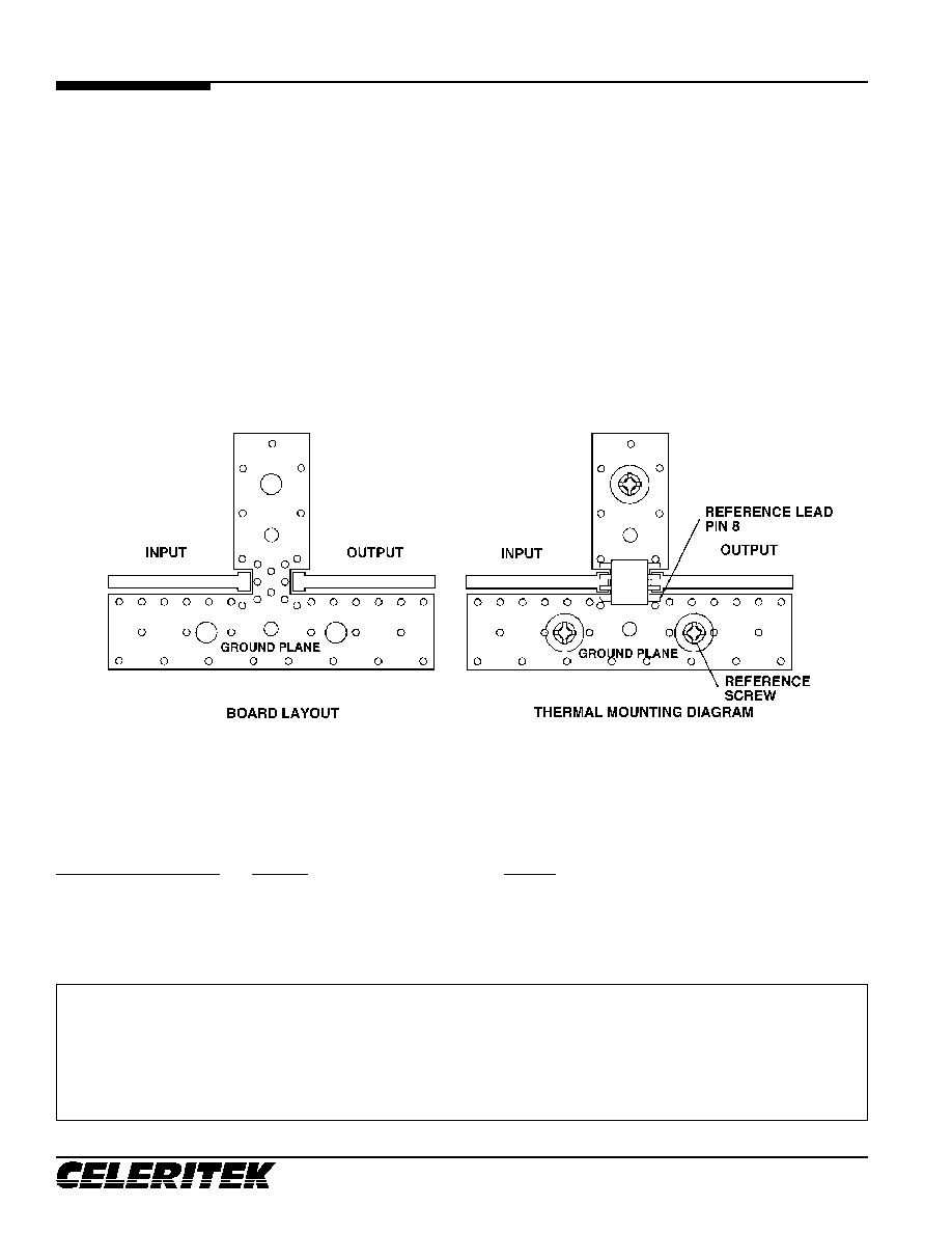
Thermal Considerations
The data shown was taken on a 31 mil thick FR-4 board with 1 ounce copper on both sides. The board was mounted to a base-
plate with 3 screws as shown. The screws bring the top side copper temperature to the same value as the baseplate. The thermal
resistance to the indicated reference lead,
JL, is 10∞C/W. The thermal resistance to the reference screw is 12∞C/W.
1. Use 1 or 2 ounce copper if possible.
2. Solder all eight leads of the CFK2162-P5 package to the appropriate electrical connection.
3. Solder the copper pad on the backside of the CFK2162-P5 package to the ground plane.
4. Use a large ground pad area with many plated through-holes as shown.
5. If possible, use at least one screw no more than 0.2 inches from the CFK2162-P5 package to provide a low thermal resistance
path to the baseplate of the package.