 | –≠–ª–µ–∫—Ç—Ä–æ–Ω–Ω—ã–π –∫–æ–º–ø–æ–Ω–µ–Ω—Ç: CHP2230 | –°–∫–∞—á–∞—Ç—å:  PDF PDF  ZIP ZIP |
3236 Scott Boulevard
Santa Clara, California 95054
Phone: (408) 986-5060
Fax: (408) 986-5095
CHP2230-PM
Features
InGaP HBT Technology
6mm Square, 50 Ohm Power Module Package
33% Linear Power Added Efficiency
+27 dBm Output Power (IS-98 WCDMA Mode)
28.5 dB Gain at Operating Output Power
On-Board Power Down Mode
Independant Gain Control via Vg adj
Independant Current Control via Vi adj
Applications
UMTS Handsets
Wireless Local Loop Subscriber Units
Description
The CHP2230-PM is a 50 ohm matched, single sup-
ply, linear power amplifier module intended for use in UMTS
handsets and wireless local loop subscriber units. The highly
integrated amplifier meets the requirements of UMTS
(WCDMA) systems. It is a member of Celeritek's new
TrueTriangleTM family of 3V power amplifier modules.
The CHP2230-PM features additional flexibility pro-
viding independent gain and current adjustments maximizing
efficiency and performance in high and low modes of opera-
tion
The CHP2230-PM is packaged in a low-cost, space
efficient, 6mm square, matched module that provides excellent
electrical stability and low thermal resistance. The module
operates from a fixed positive voltage and requires no external
matching which significantly reduces space, cost and enhances
ease of use.
The 6mm x 6mm package is self contained, incorpo-
rating 50 Ohm input and output matching networks optimized
for output power, linearity and efficiency.
Celeritek's InGaP HBT technology offers a thermally
robust and reliable PAM (power amplifier module) solution.
1.92 to 1.98 GHz
3.5V, 27.0 dBm, UMTS
InGaP HBT Amplifier Module
Advanced Product Information
July 2002
(1 of 4)
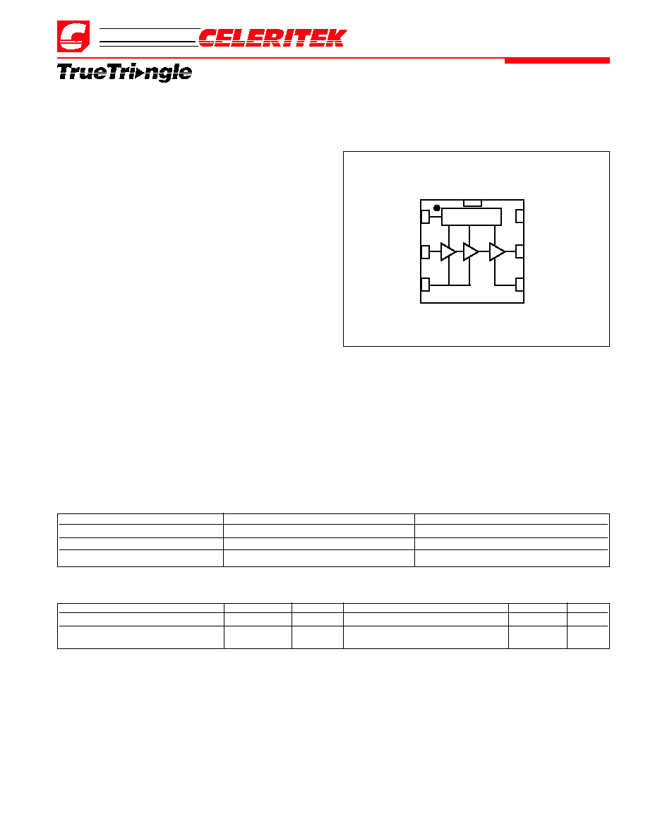
Functional Block Diagram
Application Information
The CHP2230-PM is a three-stage amplifier that requires a
single regulated positive supply along with the unregulated bat-
tery voltage for proper operation. Vref is a regulated 2.95 refer-
ence voltage for the bias control circuitry. It can also be used as
a power down mode select. Vcc is an unregulated supply volt-
age directly from the battery. Vcc should be applied prior to
Vref and before RF input power. Vi adj is a control voltage
which independently adjusts the quiescent current of the device.
In addition, the gain of the amplifier can be adjusted using a
control voltage applied to the Vg adj node. It is important that
the maximum power dissipation of the package be observed at
all times and that the maximum voltage across the device is not
exceeded.
Circuit Design Considerations
Biasing The positive Vcc supply voltages are applied to pins
3 and 4. Most bypass decoupling is provided on-board. Vref is
applied to pin 1.
The recommended DC bypass capacitance is shown in the
schematic diagram on Page 3.
≠ Continued on Page 2 ≠
TM
Absolute Maximum Ratings
Parameter
Rating
Parameter
Rating
Parameter
Rating
Collector Voltage (+Vcc)
+5.0 V*
Reference Voltage (Vref)
+3.1 V
Operating Temperature
-40∞C to +100∞C
Collector Current (Icc)
1.2 A
Power Dissipation
5 W
Storage Temperature
-65∞C to +150∞C
RF Input Power
7 dBm
V Mode
+3.1 V
Soldering Temperature
260∞C for 5 Sec.
Recommended Operating Conditions
Parameter
Typ
Units
Parameter
Typ
Units
Collector Voltage (+Vcc)
3.1 to 4.2
Volts
Operating Temperature (PC Board)
-20 to +70
∞C
Reference Voltage (Vref)
+2.95 (±1.2%)
Volts
Mode Control Voltage (Vmode)
High
2.2
V
(Fixed and regulated)
Low
1.1
V
* RF Off.
Vref 1
RF IN 2
Vcc 3
6 Vi adj
5 RF OUT
4 Vcc
Ground connection is
on backside
BIAS
7 Vg adj

3236 Scott Boulevard, Santa Clara, California 95054
Phone: (408) 986-5060
Fax: (408) 986-5095
CHP2230-PM
Advanced Product Information - July 2002
(2 of 4)
Parameter
Condition
Min
Typ
Max
Units
Frequency Range
1.92
1.98
GHz
Gain
Pout = 26.5 dBm
Vmode = High
28.5
dB
Pout = 19.0 dBm
Vmode = Low
18
20
dB
Gain Ripple*
1.92-1.98 GHz
1.0
dB
Gain Variation
Over supply voltage (3.1 to 4.2V)
-1.0 to 0.3
dB
Over temperature
-1.0 to 1.2
dB
Power Output
WCDMA mode
+26.5
+27.0
dBm
Harmonics
2nd @ Po = +28.5 dBm
-30
dBc
3rd @ Po = +28.5 dBm
-35
dBc
Linearity (ACPR)
WCDMA mode @ +26.5 dBm Pout, 5 MHz offset
-40
dBc/30KHz
WCDMA mode @ +26.5dBm Pout, 10 MHz offset
-50
dBc/30KHz
Ruggedness
6:1 VSWR @ 28.5 dBm Pout
≠
no damage
≠
≠
Noise Figure
5.0
dB
Input Return Loss
-10
dB
Efficiency
Pout = +27.0 dBm - WCDMA
30
33
%
Positive Supply Current (Icc)
Pout = +27.0 dBm - WCDMA
440
mA
Quiescent Current (Iq)
No RF, Vmode = High
65
mA
No RF, V mode = Low
45
Vref Supply Current (Iref)
6.0
10.0
mA
Vref Supply Voltage (Vref)
Fixed and regulated (1.1% tolerance)
2.95
V
Vmode
Vmode = Low
0.1
0.4
V
Vmode
Vmode = High
2.85
3.0
3.15
V
Imode
Vmode = High
400
800
µA
Leakage Current
Vref = 0V, Vcc = 3.5V
10
µA
Electrical Characteristics
Unless otherwise specified, the following specifications are guaranteed at room temperature with collector voltage (+Vcc) = 3.5 V.
* Specifications guaranteed over the temperature range of -20∞C to +70∞C
Inadequate bypass capacitance and inductance around the
DC supply lines can compromise the adjacent channel power
ratio (ACPR), reduce power gain and/or create oscillations.
Modulation When biased as specified, the CHP2230-PM will
achieve the required adjacent channel response for the digital
system specified. Celeritek tests each product under digital
modulation to ensure correlation to customer applications.
Thermal
1. The ground pad on the backside of the CHP2230-PM must
be soldered to the ground plane.
2. All leads of the package must be soldered to the appropriate
electrical connection.
Physical Dimensions and PCB Footprint
Contact the factory for detailed information and dimensions of
HBT power module package and recommended printed circuit
board footprint.
≠ Continued from Page 1 ≠
TM

3236 Scott Boulevard
Santa Clara, California 95054
Phone: (408) 986-5060
Fax: (408) 986-5095
CHP2230-PM
Advanced Product Information - July 2002
(3 of 4)
Recommended Application Circuit
Note: This schematic represents the topology of the application circuit recommended by Celeritek.
Evaluation Board Schematic
Board substrate:
ER = 4.60
Thickness = 0.031 in.
TM
PCB Footprint (Minimum Pad Dimensions)
0.015 (0.38) DIA.
VIA HOLE X21
0.032 (0.80)
MIN. X7
0.240
(6.10)
0.060 (1.50) MIN.
0.295 (7.50)
0.100 (2.55)
0.054 (1.36) X4
DIMENSIONS IN INCHES (mm)
DRAWING NOT TO SCALE
0.015 (0.40)
RADIUS
X14
RF OUT
50
Vref
Vcc
RF IN
CHP2230-PM
50
3.9 pF
3.3 µF
3.3µF
1
2
3
4
5
6
3.3 µF
Vg
3.3µF
Vi adj
7

3236 Scott Boulevard, Santa Clara, California 95054
Phone: (408) 986-5060
Fax: (408) 986-5095
CHP2230-PM
Advanced Product Information - July 2002
(4 of 4)
Celeritek reserves the right to make changes without further notice to any products herein. Celeritek makes no warranty, representation or guarantee regarding the
suitability of its products for any particular purpose, nor does Celeritek assume any liability arising out of the application or use of any product or circuit, and specifically
disclaims any and all liability, including without limitation consequential or incidental damages. "Typical" parameters can and do vary in different applications. All operating
parameters, including "Typicals" must be validated for each customer application by customer's technical experts. Celeritek does not convey any license under its patent
rights nor the rights of others. Celeritek products are not designed, intended, or authorized for use as components in systems intended for surgical implant into the body,
or other applications intended to support or sustain life, or for any other application in which the failure of the Celeritek product could create a situation where personal
injury or death may occur. Should Buyer purchase or use Celeritek products for any such unintended or unauthorized application, Buyer shall indemnify and hold Celeritek
and its officers, employees, subsidiaries, affiliates, and distributors harmless against all claims, costs, damages, and expenses, and reasonable attorney fees arising out
of, directly or indirectly, any claim of personal injury or death associated with such unintended or unauthorized use, even if such claim alleges that Celeritek was negligent
regarding the design or manufacture of the part. Celeritek is a registered trademark of Celeritek, Inc. Celeritek, Inc. is an Equal Opportunity/Affirmative Action Employer.
TM
Physical Dimensions
Ordering Information
The CHP2230-PM is available in a surface mount 50 ohm matched module and devices are available in tube or tape and reel.
Part Number for Ordering
Package
CHP2230-PM-0000
PM6 WCDMA surface mount power package in tube
CHP2230-PM-000T
PM6 WCDMA surface mount power package in tape and reel
PB-CHP2230-PM
Evaluation Board with SMA connectors FOR CHP2230-PM