2.0-18.0 GHz GaAs MMIC
Low Noise Amplifier
Page 1 of 6
Features
Self Bias Architecture
18.0 dB Small Signal Gain
3.5 dB Noise Figure
+11.0 dBm P1dB Compression Point
100% Visual Inspection to MIL-STD-883
Method 2010
General Description
Parameter
Units
GHz
dB
dB
dB
dB
dB
dB
dBm
dBm
dBm
VDC
mA
Min.
2.0
-
-
-
-
-
-
-
-
-
+4.5
90
Typ.
-
10.0
15.0
18.0
+/-1.0
40.0
3.5
+16.0
+41.0
+25.0
+5.0
105
Max.
18.0
-
-
-
-
-
-
-
-
-
+7.0
120
Supply Voltage (Vd)
Supply Current (Id)
Input Power (Pin)
Storage Temperature (Tstg)
Operating Temperature (Ta)
Channel Temperature (Tch)
+8.0 VDC
180 mA
+10 dBm
-65 to +165
O
C
-55 to MTTF Table
MTTF Table
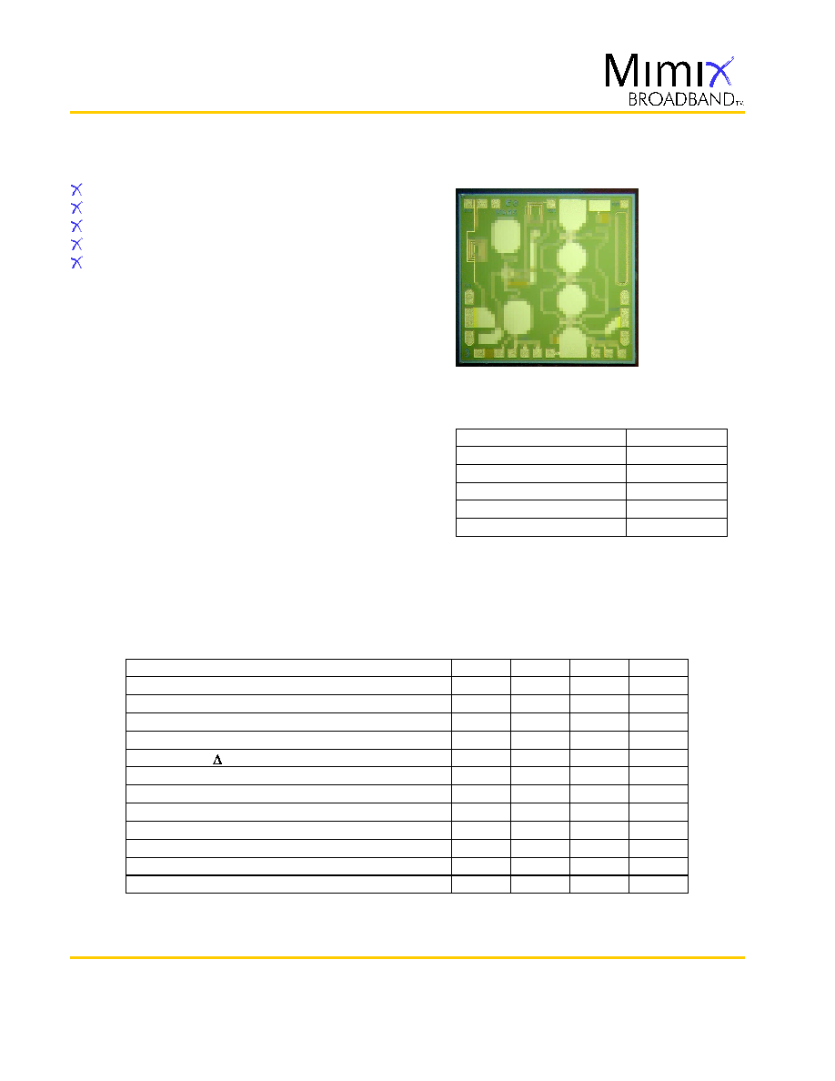
Chip Device Layout
(1) Channel temperature affects a device's MTTF. It is
recommended to keep channel temperature as low as
possible for maximum life.
1
1
Mimix Broadband, Inc., 10795 Rockley Rd., Houston, Texas 77099
Tel: 281.988.4600 Fax: 281.988.4615 mimixbroadband.com
Characteristic Data and Specifications are subject to change without notice.
©2006 Mimix Broadband, Inc.
Export of this item may require appropriate export licensing from the U.S. Government. In purchasing these parts, U.S. Domestic customers accept
their obligation to be compliant with U.S. Export Laws.
Mimix Broadband's two stage 2.0-18.0 GHz GaAs MMIC
low noise amplifier has a small signal gain of 18.0 dB
with a noise figure of 3.5 dB across the band. This MMIC
uses Mimix Broadband's 0.3 µm GaAs PHEMT device
model technology, and is based upon optical
lithography to ensure high repeatability and uniformity.
The chip has surface passivation to protect and provide
a rugged part with backside via holes and gold
metallization to allow either a conductive epoxy or
eutectic solder die attach process. This device is well
suited for fiber optic, microwave radio, military, space,
telecom infrastructure, test instrumentation and VSAT
applications.
Electrical Characteristics (Ambient Temperature T = 25
o
C)
Absolute Maximum Ratings
Frequency Range (f )
Input Return Loss (S11)
Output Return Loss (S22)
Small Signal Gain (S21)
Gain Flatness ( S21)
Reverse Isolation (S12)
Noise Figure (NF)
Output Power for 1 dB Compression (P1dB)
Output Second Order Intercept Point (OIP2)
Output Third Order Intercept Point (OIP3)
Drain Bias Voltage (Vd1,2)
Supply Current (Id) (Vd1,2=5.0V)
CMM1100
May 2006 - Rev 01-May-06
100% on-wafer DC testing and 100% RF wafer qualification. Wafer qualification includes sample testing from each quadrant
with an 80% pass rate required.
Page 2 of 6
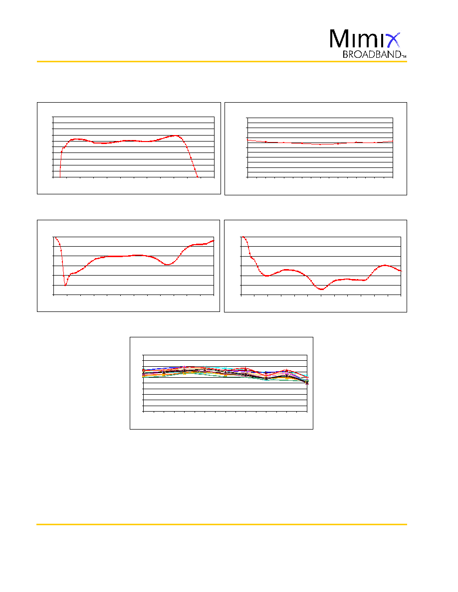
Low Noise Amplifier Measurements
2.0-18.0 GHz GaAs MMIC
Low Noise Amplifier
Mimix Broadband, Inc., 10795 Rockley Rd., Houston, Texas 77099
Tel: 281.988.4600 Fax: 281.988.4615 mimixbroadband.com
Characteristic Data and Specifications are subject to change without notice.
©2006 Mimix Broadband, Inc.
Export of this item may require appropriate export licensing from the U.S. Government. In purchasing these parts, U.S. Domestic customers accept
their obligation to be compliant with U.S. Export Laws.
CMM1100
May 2006 - Rev 01-May-06
CMM1100 Vd=5.0 V Id=110 mA
12
13
14
15
16
17
18
19
20
21
22
0.0 2.0 4.0 6.0 8.0 10.0 12.0 14.0 16.0 18.0 20.0 22.0 24.0
Frequency (GHz)
G
a
in
(
d
B
)
CMM1100 Vd=5.0 V Id=105 mA
0.0
1.0
2.0
3.0
4.0
5.0
6.0
2.0 3.0 4.0 5.0 6.0 7.0 8.0 9.0 10.0 11.0 12.0 13.0 14.0 15.0 16.0 17.0 18.0
Frequency (GHz)
No
i
s
e
F
i
g
u
r
e
(d
B
)
CMM1100 Vd=5.0 V Id=110 mA
-30
-25
-20
-15
-10
-5
0
0.0 2.0 4.0 6.0 8.0 10.0 12.0 14.0 16.0 18.0 20.0 22.0 24.0
Frequency (GHz)
I
nput
R
e
t
u
r
n
Los
s
(
d
B
)
CMM1100 Vd=5.0 V Id=110 mA
-30
-25
-20
-15
-10
-5
0
0.0 2.0 4.0 6.0 8.0 10.0 12.0 14.0 16.0 18.0 20.0 22.0 24.0
Frequency (GHz)
Ou
t
p
u
t
R
e
t
u
rn
L
o
s
s
(
d
B
)
CMM1100 Vd=5.0 V Id=115 mA
Several Devices Over Multiple Wafers
10
11
12
13
14
15
16
17
18
19
20
2.0 3.0 4.0 5.0 6.0 7.0 8.0 9.0 10.0 11.0 12.0 13.0 14.0 15.0 16.0 17.0 18.0
Frequency (GHz)
O
u
t
p
u
t
Po
w
e
r
P1
d
B
(
d
B
m
)
Page 3 of 6
S-Parameters
2.0-18.0 GHz GaAs MMIC
Low Noise Amplifier
Mimix Broadband, Inc., 10795 Rockley Rd., Houston, Texas 77099
Tel: 281.988.4600 Fax: 281.988.4615 mimixbroadband.com
Characteristic Data and Specifications are subject to change without notice.
©2006 Mimix Broadband, Inc.
Export of this item may require appropriate export licensing from the U.S. Government. In purchasing these parts, U.S. Domestic customers accept
their obligation to be compliant with U.S. Export Laws.
CMM1100
May 2006 - Rev 01-May-06
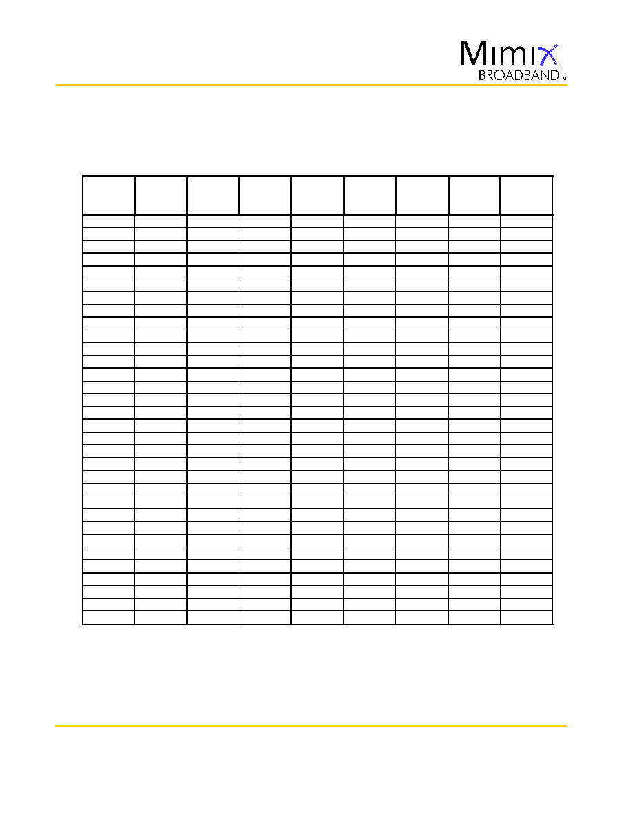
Typcial S-Parameter Data for CMM1100
V
d=5.0 V Id=110 m
A
Frequency
S11
S11
S21
S21
S12
S12
S22
S22
(GHz)
(Mag)
(Ang)
(Mag)
(Ang)
(Mag)
(Ang)
(Mag)
(Ang)
0.1
0.989
-32.89
0.002
-72.42
0.001
2.94
0.996
-14.02
0.5
0.839
-138.78
0.063
-3.31
0.002
84.86
0.936
-70.70
1.0
0.430
96.36
4.612
-156.47
0.007
-89.29
0.533
-150.27
2.0
0.079
-79.78
7.309
54.69
0.001
93.66
0.235
173.76
3.0
0.117
-123.97
7.967
-13.21
0.002
95.25
0.111
166.37
4.0
0.146
-120.27
7.957
-61.49
0.003
57.01
0.093
-178.76
5.0
0.198
-119.04
7.774
-101.59
0.004
26.90
0.110
-173.73
6.0
0.257
-127.62
7.527
-137.51
0.004
3.56
0.127
179.58
7.0
0.292
-138.75
7.397
-169.02
0.005
-21.72
0.135
162.34
8.0
0.307
-147.41
7.406
159.75
0.006
-40.36
0.125
144.68
9.0
0.308
-154.14
7.525
128.76
0.006
-62.38
0.103
122.29
10.0
0.312
-158.91
7.689
97.15
0.006
-83.34
0.070
94.80
11.0
0.318
-163.15
7.783
64.72
0.007
-104.97
0.037
42.36
12.0
0.333
-171.93
7.765
32.07
0.008
-125.80
0.037
-40.62
13.0
0.328
178.87
7.672
0.03
0.008
-149.13
0.061
-90.19
14.0
0.300
161.11
7.740
-31.97
0.009
-169.78
0.078
-114.06
15.0
0.277
142.05
7.945
-64.56
0.009
170.64
0.081
-134.69
16.0
0.184
112.04
8.293
-100.09
0.010
149.19
0.081
-148.84
17.0
0.158
55.01
8.667
-138.53
0.010
122.11
0.072
-162.15
18.0
0.191
8.33
8.929
178.72
0.011
93.61
0.054
164.21
19.0
0.341
-26.19
8.632
129.48
0.011
56.71
0.042
62.03
20.0
0.525
-54.25
7.041
76.86
0.010
15.10
0.116
-24.48
21.0
0.631
-81.75
4.883
29.71
0.009
-25.82
0.179
-69.96
22.0
0.648
-98.09
3.473
-12.54
0.008
-62.11
0.195
-99.10
23.0
0.680
-107.84
2.454
-59.85
0.008
-95.55
0.175
-122.33
24.0
0.785
-119.97
1.265
-113.21
0.006
-142.49
0.151
-130.57
25.0
0.783
-140.30
0.532
-141.73
0.005
-167.88
0.121
-132.85
26.0
0.570
-165.99
0.214
-149.82
0.003
145.82
0.113
-134.43
27.0
0.300
-94.21
0.223
-152.16
0.001
-153.86
0.105
-133.33
28.0
0.727
-114.15
0.140
170.89
0.003
176.63
0.087
-129.04
29.0
0.819
-131.21
0.074
153.50
0.004
155.26
0.078
-116.79
30.0
0.850
-142.42
0.043
147.08
0.003
151.90
0.090
-96.48

Page 4 of 6
Mechanical Drawing
Bias Arrangement
Bypass Capacitors
- See App Note [2]
(Note: Engineering designator is M425)
Units: millimeters (inches) Bond pad dimensions are shown to center of bond pad.
Thickness: 0.076 +/- 0.010 (0.003 +/- 0.0004), Backside is ground, Bond Pad/Backside Metallization: Gold
All DC Bond Pads are 0.080 x 0.080 (0.003 x 0.003). All RF Bond Pads are 0.180 x 0.080 (0.007 x 0.003).
Bond pad centers are approximately 0.109 (0.004) from the edge of the chip.
Dicing tolerance: +/- 0.005 (+/- 0.0002). Approximate weight: 1.538 mg
Bond Pad #1 (RF In)
Bond Pad #2 (Vg1a)
Bond Pad #3 (Vg1b)
Bond Pad #4 (Vd1)
Bond Pad #5 (Vd2)
Bond Pad #6 (RF Out)
2.0-18.0 GHz GaAs MMIC
Low Noise Amplifier
Mimix Broadband, Inc., 10795 Rockley Rd., Houston, Texas 77099
Tel: 281.988.4600 Fax: 281.988.4615 mimixbroadband.com
Characteristic Data and Specifications are subject to change without notice.
©2006 Mimix Broadband, Inc.
Export of this item may require appropriate export licensing from the U.S. Government. In purchasing these parts, U.S. Domestic customers accept
their obligation to be compliant with U.S. Export Laws.
CMM1100
May 2006 - Rev 01-May-06
6
1
7
1.550
(0.061)
0.418
(0.017)
2
1.460
(0.058)
0.0
0.0
1.600
(0.063)
1.480
(0.058)
8
1.360
(0.054)
9
1.245
(0.049)
10
0.714
(0.028)
11
0.599
(0.024)
12
0.484
(0.019)
3
0.215
(0.009)
4
0.843
(0.033)
5
1.508
(0.059)
0.418
(0.017)
Bond Pad #7 (Rs2-9.0 )
Bond Pad #8 (Rs2-12.5 )
Bond Pad #9 (Rs2-12.5 )
Bond Pad #10 (Rs1-29.0 )
Bond Pad #11 (Rs1-29.0 )
Bond Pad #12 (Rs1-16.6 )
6
1
7
2
8
9
10
11
12
3
4
5
Vd1,2
RF In
RF Out
Page 5 of 6
App Note [1] Biasing
- As shown in the bonding diagram, this device operates using a self-biased architecture and only requires one drain
bias. Bias is nominally Vd1=Vd2=5V, I
TOTAL
=105mA. Additionally there are six total source resistors on chip. The three resistors on the input
stage are 16.6, 29.0 and 29.0 Ohms. The three resistors on the output stage are 12.5, 12.5 and 9.0 Ohms. One of these must be bonded to
ground for each amplifier stage to achieve performance as shown. Bonding to one of the other resistors or any or all in parallel may allow
additional performance adjustment. Lastly for additional stability pad #3 can be grounded instead of bond pad #2.
App Note [2] Bias Arrangement
- Each DC pad (Vd) needs to have DC bypass capacitance (~100-200 pF) as close to the device as possible.
Additional DC bypass capacitance (~0.01 uF) is also recommended.
Device Schematic
2.0-18.0 GHz GaAs MMIC
Low Noise Amplifier
Mimix Broadband, Inc., 10795 Rockley Rd., Houston, Texas 77099
Tel: 281.988.4600 Fax: 281.988.4615 mimixbroadband.com
Characteristic Data and Specifications are subject to change without notice.
©2006 Mimix Broadband, Inc.
Export of this item may require appropriate export licensing from the U.S. Government. In purchasing these parts, U.S. Domestic customers accept
their obligation to be compliant with U.S. Export Laws.
CMM1100
May 2006 - Rev 01-May-06
Backplate
Temperature
55 deg Celsius
75 deg Celsius
95 deg Celsius
Channel
Temperature
deg Celsius
deg Celsius
deg Celsius
FITs
E+
E+
E+
MTTF Hours
E+
E+
E+
Rth
C/W
C/W
C/W
Bias Conditions: Vd1,2=5.0V, I
TOTAL
=105 mA
These numbers were calculated based on accelerated life test information and thermal model analysis received from the fabricating foundry.
MTTF Table (TBD)
(Thermal Resistance (Rth) is 60.0∫C/W)

Page 6 of 6
Handling and Assembly Information
CAUTION! - Mimix Broadband MMIC Products contain gallium arsenide (GaAs) which can be hazardous to the
human body and the environment. For safety, observe the following procedures:
Do not ingest.
Do not alter the form of this product into a gas, powder, or liquid through burning, crushing, or chemical
processing as these by-products are dangerous to the human body if inhaled, ingested, or swallowed.
Observe government laws and company regulations when discarding this product. This product must be
discarded in accordance with methods specified by applicable hazardous waste procedures.
Life Support Policy - Mimix Broadband's products are not authorized for use as critical components in life support
devices or systems without the express written approval of the President and General Counsel of Mimix Broadband. As
used herein: (1) Life support devices or systems are devices or systems which, (a) are intended for surgical implant into
the body, or (b) support or sustain life, and whose failure to perform when properly used in accordance with
instructions for use provided in the labeling, can be reasonably expected to result in a significant injury to the user.
(2) A critical component is any component of a life support device or system whose failure to perform can be
reasonably expected to cause the failure of the life support device or system, or to affect its safety or effectiveness.
ESD - Gallium Arsenide (GaAs) devices are susceptible to electrostatic and mechanical damage. Die are supplied in
antistatic containers, which should be opened in cleanroom conditions at an appropriately grounded antistatic work-
station. Devices need careful handling using correctly designed collets, vacuum pickups or, with care, sharp tweezers.
Die Attachment - GaAs Products from Mimix Broadband are 0.076 mm (0.003") thick and have vias through to the
backside to enable grounding to the circuit. Microstrip substrates should be brought as close to the die as possible. The
mounting surface should be clean and flat. If using conductive epoxy, recommended epoxy is Tanaka TS3332LD cured
in a nitrogen atmosphere per manufacturer's cure schedule. Apply epoxy sparingly to avoid getting any on to the top
surface of the die. An epoxy fillet should be visible around the total die periphery. If eutectic mounting is preferred,
then a fluxless gold-tin (AuSn) preform, approximately 0.001
2
thick, placed between the die and the attachment surface
should be used. A die bonder that utilizes a heated collet and provides scrubbing action to ensure total wetting to
prevent void formation in a nitrogen atmosphere is recommended. The gold-tin eutectic (80% Au 20% Sn) has a
melting point of approximately 280∫ C (Note: Gold Germanium should be avoided). The work station temperature
should be 310∫C +/- 10∫C. Exposure to these extreme temperatures should be kept to minimum. The collet should be
heated, and the die pre-heated to avoid excessive thermal shock. Avoidance of air bridges and force impact are critical
during placement.
Wire Bonding - Windows in the surface passivation above the bond pads are provided to allow wire bonding to the
die's gold bond pads. The recommended wire bonding procedure uses 0.076 mm x 0.013 mm (0.003" x 0.0005") 99.99%
pure gold ribbon with 0.5-2% elongation to minimize RF port bond inductance. Gold 0.025 mm (0.001") diameter
wedge or ball bonds are acceptable for DC Bias connections. Aluminum wire should be avoided. Thermo-compression
bonding is recommended though thermosonic bonding may be used providing the ultrasonic content of the bond is
minimized. Bond force, time and ultrasonics are all critical parameters. Bonds should be made from the bond pads on
the die to the package or substrate. All bonds should be as short as possible.
2.0-18.0 GHz GaAs MMIC
Low Noise Amplifier
Mimix Broadband, Inc., 10795 Rockley Rd., Houston, Texas 77099
Tel: 281.988.4600 Fax: 281.988.4615 mimixbroadband.com
Characteristic Data and Specifications are subject to change without notice.
©2006 Mimix Broadband, Inc.
Export of this item may require appropriate export licensing from the U.S. Government. In purchasing these parts, U.S. Domestic customers accept
their obligation to be compliant with U.S. Export Laws.
CMM1100
May 2006 - Rev 01-May-06
Part Number for Ordering
Description
CMM1100-BD
RoHS compliant die packed in gel paks
PB-CMM1100-BD
CMM1100-BD
evaluation
module