
mOE"OEY@b~Ј,,...,,"L@i"N@QPWYU@rЈ`'^ @rNL@hЈ>TMsЈ"L@t^Y,,TM@WWPYY
t^'Z@RXQNYXXNTVPP@@f,,YZ@RXQNYXXNTVQU@@zzzN"OE"OEY...~Ј,,...,,"NЈ"
–RPPU@mOE"OEY@b~Ј,,...,,"L@i"N
CMM3030-BD
SP@`h°@sЈ@SP@gh°@g,,aTM@mmic
o≠sOE,,'@mЈ>',,sЈ~@d~OEoe^~@a"≠'OE^~
3236 Scott Boulevard
Santa Clara, California 95054
Phone: (408) 986-5060
Fax: (408) 986-5095
CMM3030-BD
Features
Small Size
High Gain: 9 dB Typical
Output Voltage up to 7.5 V Peak-to-Peak
30 kHz to 30 GHz Bandwidth
Low Gain Ripple: 1.0 dB pp Typical
Sub 0.25 Micron PHEMT
Applications
Driver Amplifier for LiNb03 Modulator @
OC192 bit rate SONET/SHD Transmission
Systems
Medium Power Linear Gain Block for
Broadband Systems
Description
The CMM3030-BD is a precision GaAs MMIC,
medium power amplifier and is part of Celeritek's family of
WideFiberTM products.
The CMM3030-BD optical driver amplifier gives
fiber optic system designers a unique combination of wide-
band frequency coverage, along with a flat response and very
low internal jitter. It is a precision PHEMT GaAs MMIC
medium power amplifier with +23 dBm @ P1dB. It operates
from 30 kHz to 30 GHz with a 9 dB linear gain. Low internal
jitter makes it especially well suited for high speed digital
data applications. Maximum output voltage is 7.5 V peak-to-
peak.
It is an excellent choice as a driver amplifier for
Lithium Niobate (Mach-Zehnder) external optical modulators,
to achieve high extinction ratio. Targeted for OC-192/STM64
metropolitan and long-haul dense wave-division multiplexed
optical networking applications and other high speed applica-
tions. The bit rate can be as high as 15 Gb/s to provide over-
head for forward error-correction algorithms. The bias voltage
can be adjusted to reduce the output voltage as needed.
CMM3030-BD amplifiers are shipped in Gel Pack
from Celeritek's foundry.
30 kHz to 30 GHz GaAs MMIC
Optical Modulator Driver Amplifier
Advanced Product Information
February 2002
(1 of 2)
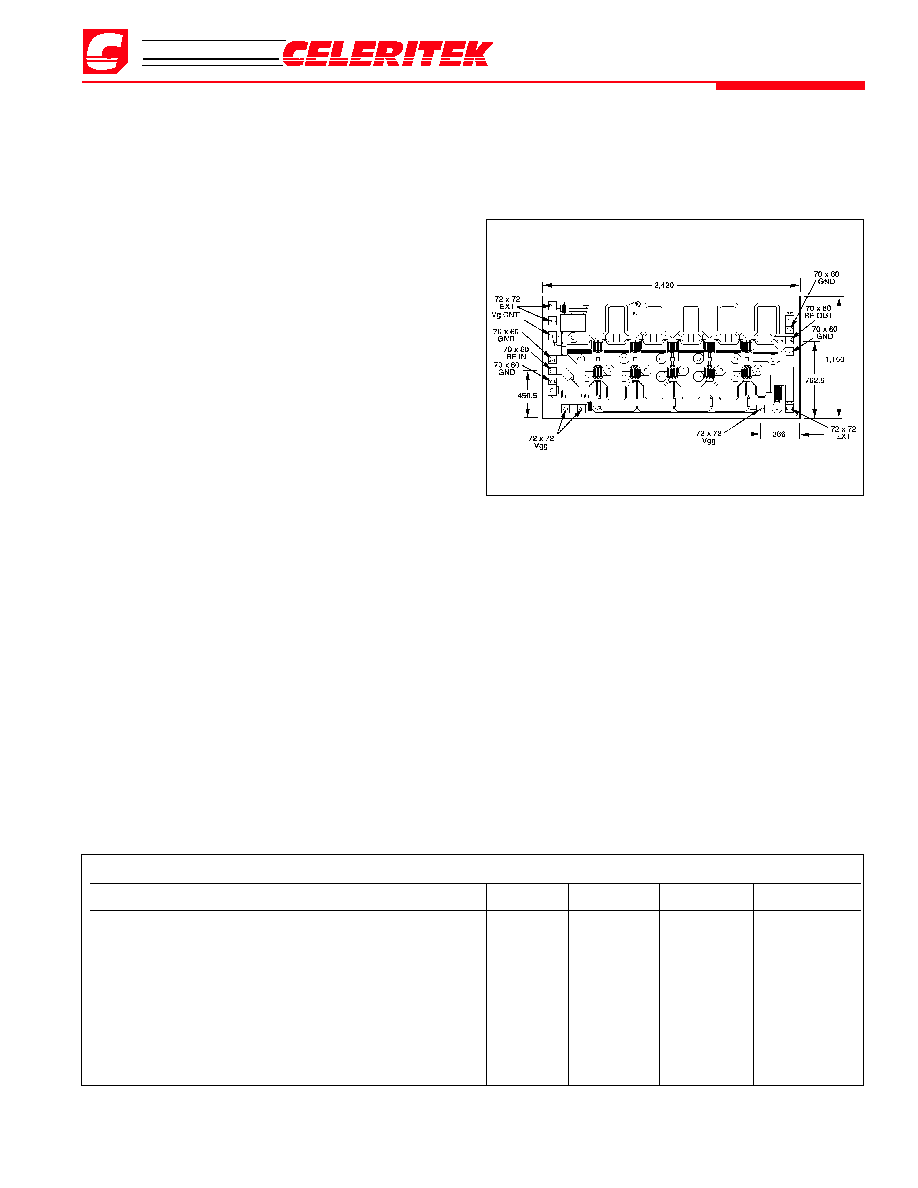
Chip Diagram
Specifications (TA = 25∞C, VDD = 8V)
(On-Wafer Probe)
Parameters
Units
Min
Typ
Max
Frequency Range
--
30 kHz
30.0 GHz
Small Signal Gain
dB
8.0
9.0
Gain Flatness
±dB
0.5
0.75
Input/Output VSWR
--
1.8:1
2.0:1
Power Output (@1 dB Gain Compression) @ 12 GHz
dBm
22.0
24.0
Second Order Intercept Point @ 12 GHz
dBm
40.0
Third Order Intercept Point @ 12 GHz
dBm
30.0
Current
mA
275
350
Units in Microns
3236 Scott Boulevard, Santa Clara, California 95054
Phone: (408) 986-5060
Fax: (408) 986-5095
CMM3030-BD
Advanced Product Information - February 2002
(2 of 4)
Absolute Maximum Ratings
Parameter
Rating
Drain Voltage
12 V
Gate Voltage
-5 V
Drain Current
375 mA
Continuous Power Dissipation
3.0 W
Channel Temperature
+175∞C
Storage Temperature
-65∞C to +175∞C
Mounting Temperature
+320∞C
Input Power
+23 dBm
Die Attach and Bonding Procedures
Die Attach: Eutectic die attach is recommended. For eutec-
tic die attach: Preform: AuSn (80% Au, 20% Sn); Stage
Temperature: 290∞C, ±5∞C; Handling Tool: Tweezers; Time: 1
min or less.
Wire Bonding: Wire Size: 0.7 to 1.0 mil in diameter (pre-
stressed); Thermocompression bonding is preferred over
thermosonic bonding. For thermocompression bonding:
Stage Temperature: 250∞C; Bond Tip Temperature: 150∞C;
Bonding Tip Pressure: 18 to 40 gms depending on size of
wire.
Performance Optimization
Using the Gain-Ctl facility of the CMM3030-BD, out-
put power may be increased by application of 1.2 to 1.8 Volts
to the Bias Control pad. If the Gain-Ctl facility is not used, a
fixed voltage at the Bias Control pad can be implemented by
connecting a off-chip parallel resistor to the pad which will
lower the output voltage accordingly.
If Bias Control voltage is decreased further than those
lowest values given in the tables, both gain and output power
will start to drop.
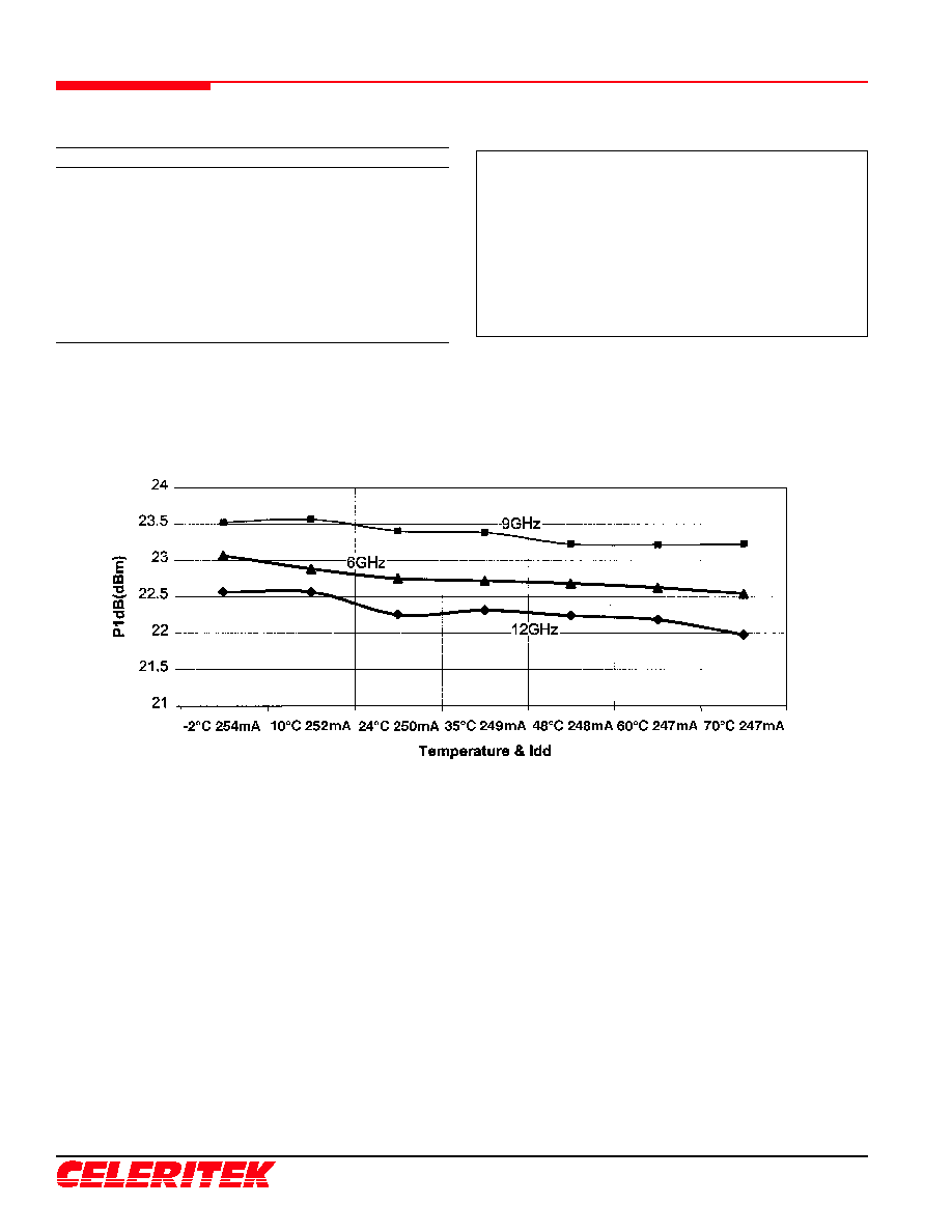
Typical Performance
P1dB vs Temperature
3236 Scott Boulevard
Santa Clara, California 95054
Phone: (408) 986-5060
Fax: (408) 986-5095
CMM3030-BD
Advanced Product Information - February 2002
(3 of 4)
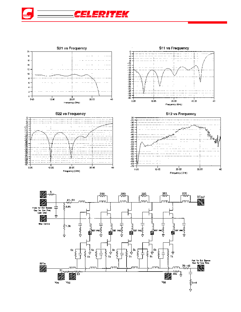
Typical Performance
Schematic Diagram
3236 Scott Boulevard, Santa Clara, California 95054
Phone: (408) 986-5060
Fax: (408) 986-5095
CMM3030-BD
Advanced Product Information - February 2002
(4 of 4)
Celeritek reserves the right to make changes without further notice to any products herein. Celeritek makes no warranty, representation or guarantee regarding the
suitability of its products for any particular purpose, nor does Celeritek assume any liability arising out of the application or use of any product or circuit, and specifically
disclaims any and all liability, including without limitation consequential or incidental damages. "Typical" parameters can and do vary in different applications. All operating
parameters, including "Typicals" must be validated for each customer application by customer's technical experts. Celeritek does not convey any license under its patent
rights nor the rights of others. Celeritek products are not designed, intended, or authorized for use as components in systems intended for surgical implant into the body, or
other applications intended to support or sustain life, or for any other application in which the failure of the Celeritek product could create a situation where personal injury
or death may occur. Should Buyer purchase or use Celeritek products for any such unintended or unauthorized application, Buyer shall indemnify and hold Celeritek and
its officers, employees, subsidiaries, affiliates, and distributors harmless against all claims, costs, damages, and expenses, and reasonable attorney fees arising out of,
directly or indirectly, any claim of personal injury or death associated with such unintended or unauthorized use, even if such claim alleges that Celeritek was negligent
regarding the design or manufacture of the part. Celeritek is a registered trademark of Celeritek, Inc. Celeritek, Inc. is an Equal Opportunity/Affirmative Action Employer.
Ordering Information
Part Number for Ordering
Description
CMM3030-BD
Optical Modulator Driver Amplifier
Bonding Sample
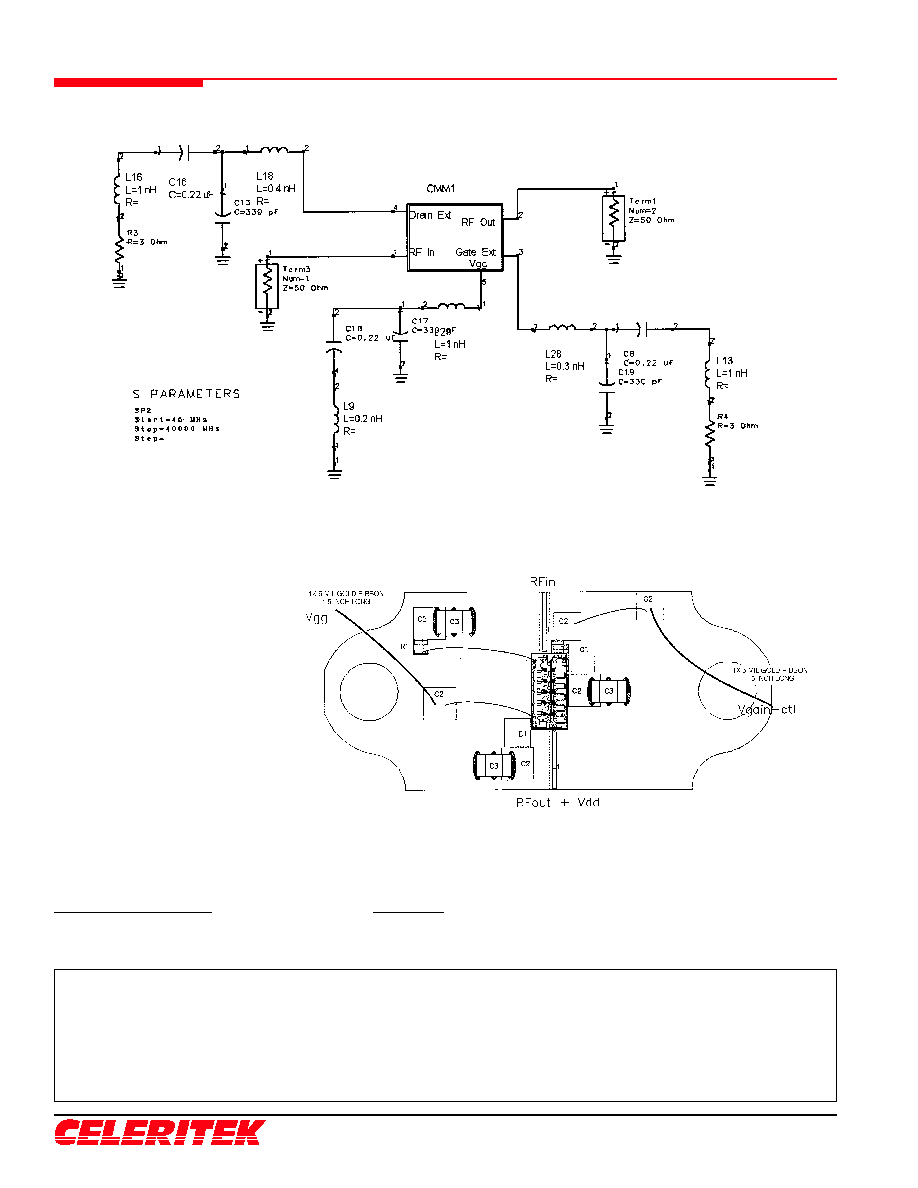
MMIC termination Circuit Design