 | ÐлекÑÑоннÑй компоненÑ: PS2513-1 | СкаÑаÑÑ:  PDF PDF  ZIP ZIP |
PS2513-1,PS2513L-1
-
NEPOC Series
-
PHOTOCOUPLER
PS2513-1,PS2513L-1
HIGH-SPEED SWITCHING/HIGH ISOLATION VOLTAGE
PHOTOCOUPLER SERIES
Document No. PN10163EJ02V0DS (2nd edition)
Date Published February 2003 CP(K)
The mark shows major revised points.
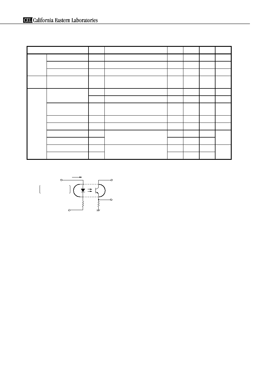
DESCRIPTION
The PS2513-1 and PS2513L-1 are optically coupled isolators containing a GaAs light emitting diode and an NPN
silicon phototransistor.
The PS2513-1 is in a plastic DIP (Dual In-line Package) and the PS2513L-1 is lead bending type (Gull-wing) for
surface mount.
FEATURES
· High isolation voltage (BV = 5 000 Vr.m.s.)
· High collector to emitter voltage (V
CEO
= 120 V)
· Guaranteed maximum switching speed (t
off
60
µ
s @ I
F
= 5 mA, V
CC
= 5 V, R
L
= 1.9 k
)
· High-speed
switching (t
on
= 5
µ
s TYP. @ I
F
= 5 mA, V
CC
= 5 V, R
L
= 1.9 k
)
(t
off
= 25
µ
s TYP. @ I
F
= 5 mA, V
CC
= 5 V, R
L
= 1.9 k
)
· Ordering number of tape product: PS2513L-1-E3, E4, F3, F4
APPLICATIONS
· Power
supply
· Air
conditioner
· FA
equipment
PS2513-1,PS2513L-1
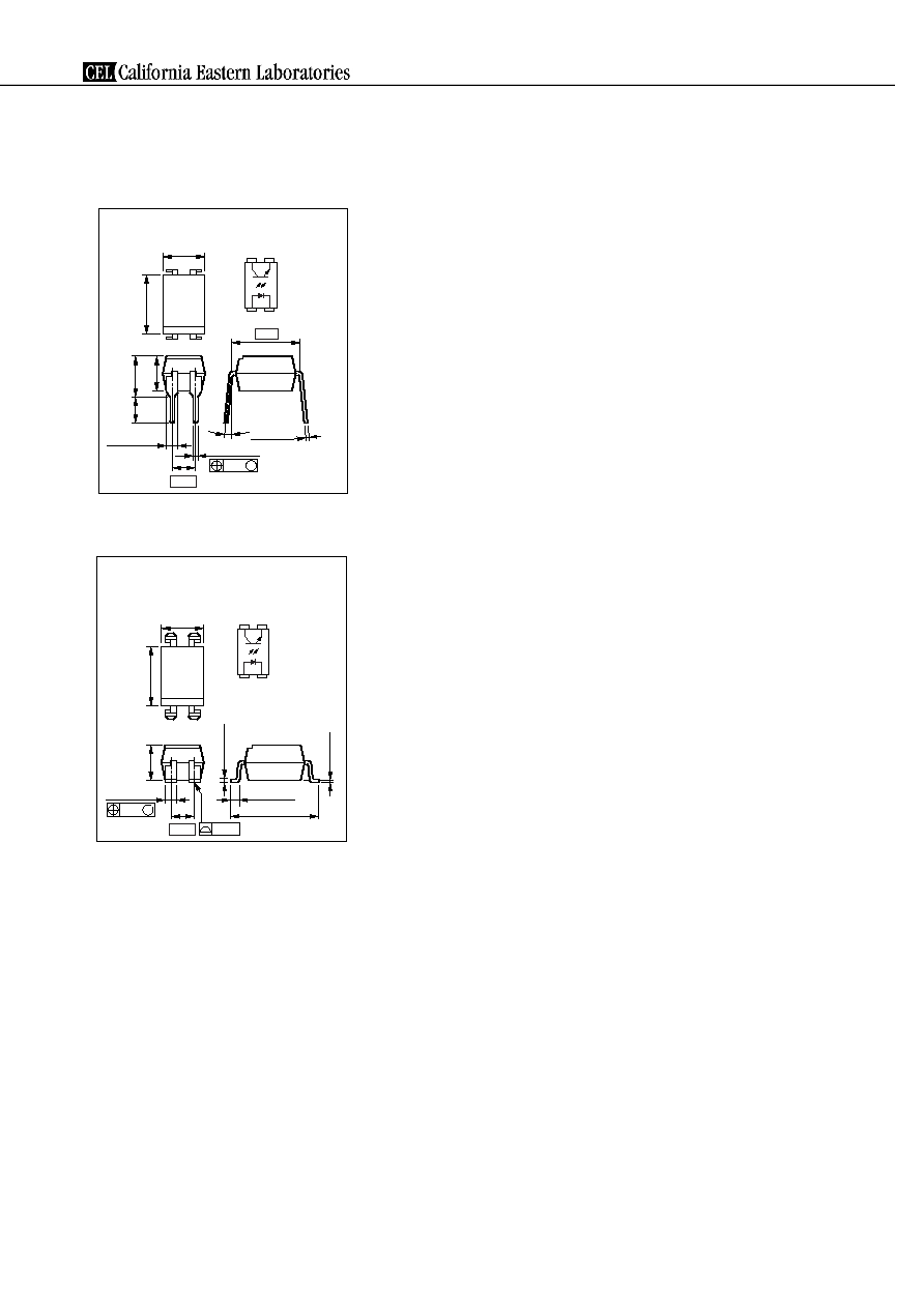
PACKAGE DIMENSIONS (UNIT: mm)
DIP Type
PS2513-1
TOP VIEW
1. Anode
2. Cathode
3. Emitter
4. Collector
3.5±0.3
4.15±0.4
3.2±0.4
2.54
1.25±0.15
0.50±0.10
0.25
M
4.6±0.35
6.5±0.5
0 to 15°
7.62
0.25
+0.1
0.05
1
2
4
3
Lead Bneding Type
PS2513L-1
TOP VIEW
0.25
M
4.6±0.35
6.5±0.5
3.5±0.3
2.54
1.25±0.15
0.15
0.9±0.25
9.60±0.4
0.25
+0.1
0.05
0.1
+0.1
0.05
1
2
4
3
1. Anode
2. Cathode
3. Emitter
4. Collector
Data Sheet PN10163EJ02V0DS
2
PS2513-1,PS2513L-1
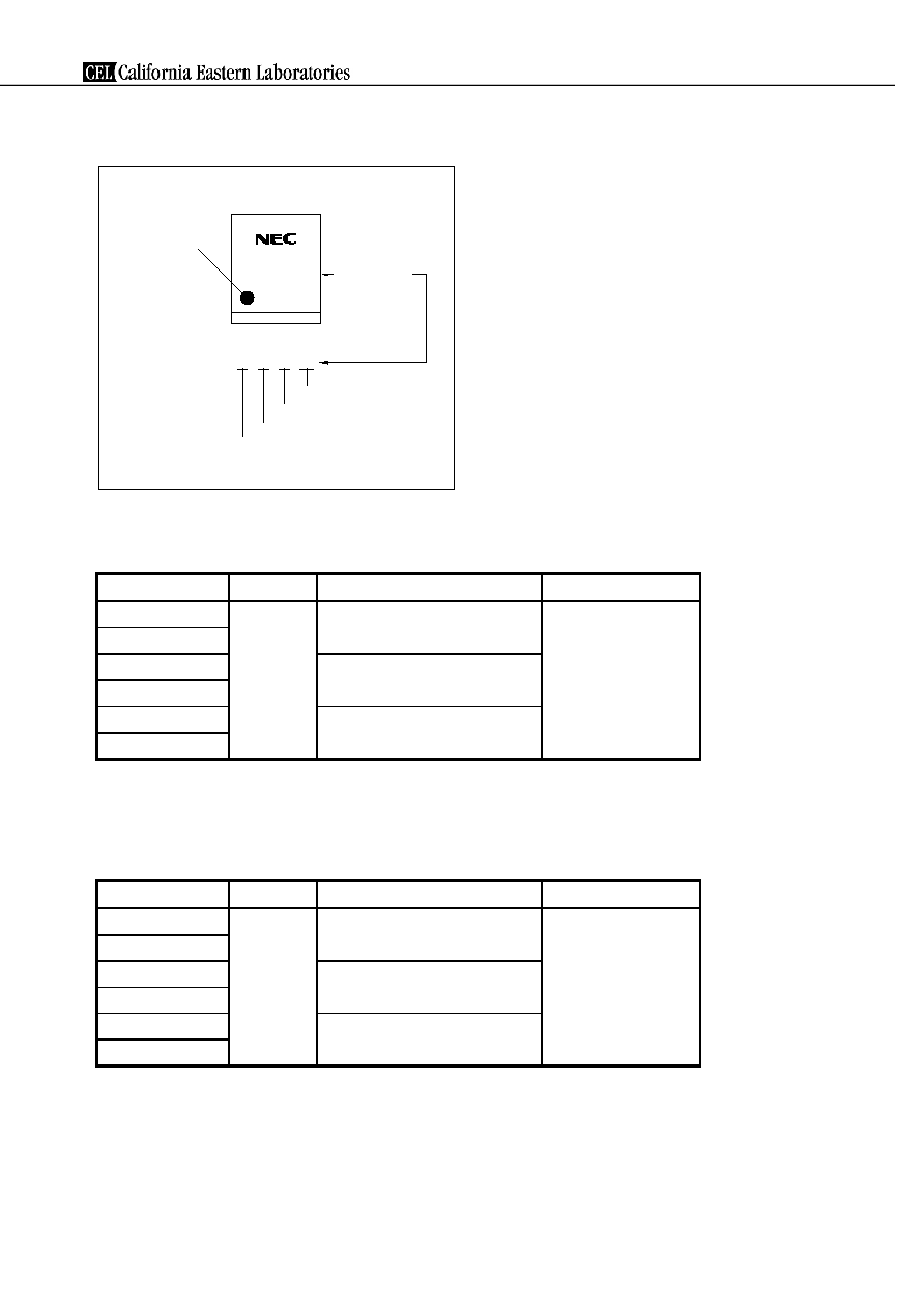
MARKING EXAMPLE
2513
NE003
Assembly Lot
Week Assembled
Year Assembled
(Last 1 Digit)
In-house Code
CTR Rank Code
No. 1 pin
Mark
N
0
03
E
ORDERING INFORMATION (Solder Contains Lead)
Part Number
Package
Packing Style
Application Part Number
*1
PS2513-1
4-pin DIP
Magazine case 100 pcs
PS2513-1
PS2513L-1
PS2513L-1-E3
Embossed Tape 1 000 pcs/reel
PS2513L-1-E4
PS2513L-1-F3
Embossed Tape 2 000 pcs/reel
PS2513L-1-F4
*1 For the application of the Safety Standard, following part number should be used.
ORDERING INFORMATION (Pb-Free)
Part Number
Package
Packing Style
Application Part Number
*1
PS2513-1-A
4-pin DIP
Magazine case 100 pcs
PS2513-1
PS2513L-1-A
PS2513L-1-E3-A
Embossed Tape 1 000 pcs/reel
PS2513L-1-E4-A
PS2513L-1-F3-A
Embossed Tape 2 000 pcs/reel
PS2513L-1-F4-A
*1 For the application of the Safety Standard, following part number should be used.
Data Sheet PN10163EJ02V0DS
3
PS2513-1,PS2513L-1
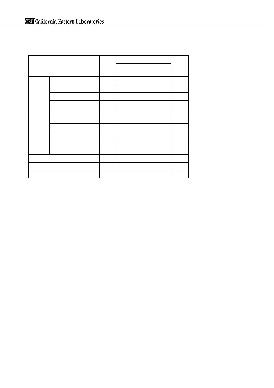
ABSOLUTE MAXIMUM RATINGS (T
A
= 25
°
C, unless otherwise specified)
Ratings
Parameter Symbol
PS2513-1,
PS2513L-1
Unit
Diode Reverse
Voltage
V
R
6 V
Forward Current (DC)
I
F
60 mA
Power Dissipation Derating
P
D
/
°
C 1.5 mW/
°
C
Power
Dissipation P
D
150 mW
Peak Forward Current
*1
I
FP
1 A
Transistor Collector to Emitter Voltage
V
CEO
120 V
Emitter to Collector Voltage
V
ECO
6 V
Collector
Current
I
C
30 mA
Power Dissipation Derating
P
C
/
°
C 1.5 mW/
°
C
Power
Dissipation P
C
150 mW
Isolation Voltage
*2
BV 5
000
Vr.m.s.
Operating Ambient Temperature
T
A
-
55 to +100
°
C
Storage Temperature
T
stg
-
55 to +150
°
C
*1 PW = 100
µ
s, Duty Cycle = 1%
*2 AC voltage for 1 minute at T
A
= 25
°
C, RH = 60% between input and output
Data Sheet PN10163EJ02V0DS
4
PS2513-1,PS2513L-1
ELECTRICAL CHARACTERISTICS (T
A
= 25
°
C)
Parameter Symbol Conditions MIN.
TYP.
MAX.
Unit
Diode Forward
Voltage
V
F
I
F
= 5 mA
1.1
1.3
V
Reverse
Current I
R
V
R
= 5 V
5
µ
A
Terminal
Capacitance
C
t
V = 0 V, f = 1.0 MHz
30
pF
Transistor Collector to Emitter Dark
Current
I
CEO
V
CE
= 120 V, I
F
= 0 mA
100
nA
Coupled
Current Transfer Ratio
CTR1
I
F
= 1 mA, V
CE
= 5 V
25
75
100
%
(I
C
/I
F
) CTR2
I
F
= 5 mA, V
CE
= 5 V
50
125
200
%
Collector
Saturation
Voltage
V
CE(sat)
I
F
= 10 mA, I
C
= 2 mA
0.3
V
Isolation
Resistance
R
I-O
V
I-O
= 1.0 kV
DC
10
11
Isolation
Capacitance
C
I-O
V = 0 V, f = 1.0 MHz
0.5
pF
Rise
Time
*1
t
r
V
CC
= 5 V, I
C
= 2 mA, R
L
= 100
3
µ
s
Fall
Time
*1
t
f
4
Turn-on
Time
*1
t
on
V
CC
= 5 V, I
F
= 5 mA, R
L
= 1.9 k
5
60
µ
s
Turn-off
Time
*1
t
off
25 60
*1 Test circuit for switching time
PW = 100 s
Duty Cycle = 1/10
µ
Pulse Input
V
CC
V
OUT
R
L
= 100
, 1.9 k
50
I
F
CAUTIONS REGARDING NOISE
Be aware that when voltage is applied suddenly between the photocoupler's input and output or between corrector-
emitters at startup, the output side may enter the on state, even if the voltage is within the absolute maximum ratings.
Data Sheet PN10163EJ02V0DS
5