 | –≠–ª–µ–∫—Ç—Ä–æ–Ω–Ω—ã–π –∫–æ–º–ø–æ–Ω–µ–Ω—Ç: PS2841-4A | –°–∫–∞—á–∞—Ç—å:  PDF PDF  ZIP ZIP |

PHOTOCOUPLER
PS2841-4A,PS2841-4B
WORLD'S SMALLEST CLASS, FOUR CHANNELS
12-PIN ULTRA SMALL SOP PHOTOCOUPLER
-
NEPOC Series
-
DESCRIPTION
The PS2841-4A and PS2841-4B are optically coupled isolators containing GaAs light emitting diodes and NPN
silicon phototransistors.
These products include four channels in a single package for high-density mounting applications.
The PS2841-4A and PS2841-4B are the world's smallest class of photocouplers and realize about 50% reduction in
mounting area compared with the PS280x and PS281x Series.
FEATURES
∑ Ultra small and thin package
(12-pin ultra small SOP, Pin pitch 0.8 mm, 4.4 (L)
◊
5.6 (W)
◊
2.5 (H))
1 2
3 4
5 6
12 11 10 9
8 7
PS2841-4A
Channel
1 ch
2 ch
3 ch
4 ch
Anode
2
3
4
5
Cathode
1, 6 common
1, 6 common
1, 6 common
1, 6 common
Emitter
11
10
9
8
Collector
7, 12 common
7, 12 common
7, 12 common
7, 12 common
PIN CONNECTIONS
(Top View)
∑ Common lead
PS2841-4A: cathode, collector common
PS2841-4B: anode, collector common
∑ High current transfer ratio (CTR = 200% TYP. @ I
F
= 1mA)
∑ High isolation voltage (BV = 1 500 Vr.m.s.)
∑ Pb-Free
product
∑ Ordering number of tape product:
PS2841-4A-F3, F4: 2 500 pcs/reel
PS2841-4B-F3, F4: 2 500 pcs/reel
∑ Safety
standards
∑ UL approved: File No. E72422
1 2
3 4
5 6
12 11 10 9
8 7
PS2841-4B
PIN CONNECTIONS
(Top View)
Channel
1 ch
2 ch
3 ch
4 ch
Anode
1, 6 common
1, 6 common
1, 6 common
1, 6 common
Cathode
2
3
4
5
Emitter
11
10
9
8
Collector
7, 12 common
7, 12 common
7, 12 common
7, 12 common
APPLICATIONS
∑ Programmable logic controllers (PLCs)
∑ Input and output for function automation
∑ Hybrid
IC
Document No. PN10202EJ03V0DS (3rd edition)
Date Published April 2005 CP(K)
The mark shows major revised points.
PS2841-4A,PS2841-4B
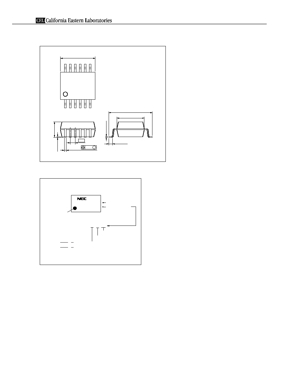
PACKAGE DIMENSIONS (UNIT: mm)
4.4
7.0±0.3
0.5±0.3
0.15
+0.10 ≠0.05
5.6±0.3
1
6
12
7
0.1±0.1
2.5
+0.3 ≠0.2
0.3±0.1
0.8
0.12
M
MARKING EXAMPLE
N 0 03
Type Number
*1
Assembly Lot
*2
No. 1 pin
Mark
2841A
N 003
Week Assembled
Year Assembled
(Last 1 Digit)
CTR Rank Code
*1 Applicable type numbers
are underlined below
PS2841-4A
PS2841-4B
*2 For the external plating Pb-Free product,
L is indicated at the second digit of the rank.
Data Sheet PN10202EJ03V0DS
2
PS2841-4A,PS2841-4B
ORDERING INFORMATION
Part Number
Order Number
Solder Plating
Specification
Packing Style
Safety Standard
Approval
Application Part
Number
*1
PS2841-4A-F3 PS2841-4A-F3
Solder
contains Embossed Tape 2 500 pcs/reel Standard products
PS2841-4A
PS2841-4A-F4 PS2841-4A-F4
lead
(UL
Approved)
PS2841-4B-F3 PS2841-4B-F3
PS2841-4B
PS2841-4B-F4 PS2841-4B-F4
PS2841-4A-F3 PS2841-4A-F3-A Pb-Free
PS2841-4A
PS2841-4A-F4 PS2841-4A-F4-A
PS2841-4B-F3 PS2841-4B-F3-A
PS2841-4B
PS2841-4B-F4 PS2841-4B-F4-A
*1 For the application of the Safety Standard, following part number should be used.
ABSOLUTE MAXIMUM RATINGS (Unless otherwise specified, T
A
= 25
∞
C)
Parameter Symbol
Ratings
Unit
Diode
Forward Current (DC)
I
F
20
mA/ch
Reverse
Voltage
V
R
6 V
Power Dissipation Derating
I
F
/
∞
C 0.2 mA
/
∞
C
Peak Forward Current
*1
I
FP
0.5 A
Transistor Collector to Emitter Voltage
V
CEO
70 V
Emitter to Collector Voltage
V
ECO
5 V
Collector
Current
I
C
20
mA/ch
Power Dissipation Derating
P
C
/
∞
C 0.4 mW/
∞
C
Power
Dissipation P
C
40
mW/ch
Isolation Voltage
*2
BV 1
500
Vr.m.s.
Operating Ambient Temperature
T
A
≠40 to +100
∞
C
Storage Temperature
T
stg
≠55 to +125
∞
C
*1 PW = 100
µ
s, Duty Cycle = 1%
*2 AC voltage for 1 minute at T
A
= 25
∞
C, RH = 60% between input and output.
Pins 1-6 shorted together, 7-12 shorted together.
Data Sheet PN10202EJ03V0DS
3

PS2841-4A,PS2841-4B
ELECTRICAL CHARACTERISTICS (T
A
= 25∞C)
Parameter Symbol
Conditions
MIN.
TYP.
MAX.
Unit
Diode Forward
Voltage
V
F
I
F
= 1 mA
0.9
1.1
1.2
V
Reverse
Current
I
R
V
R
= 5 V
10
µ
A
Terminal
Capacitance C
t
V = 0 V, f = 1 MHz
15
pF
Transistor Collector to Emitter Current
I
CEO
I
F
= 0 mA, V
CE
= 24 V
100
nA
Coupled
Current Transfer Ratio (I
C
/I
F
) CTR
I
F
= 1 mA, V
CE
= 0.4 V
100
200
400
%
Optical Leakage Current
*1
(1 to 2-ch, 2 to 3-ch, 3 to 4-ch)
I
L
I
F
= 5 mA, V
CE
= 24 V
100
nA
Collector Saturation Voltage
V
CE (sat)
I
F
= 1 mA, I
C
= 0.2 mA
0.13
0.3
V
Isolation
Resistance R
I-O
V
I-O
= 1 kV
DC
10
11
Isolation
Capacitance C
I-O
V = 0 V, f = 1 MHz
0.4
pF
Turn-on
Time
*2
t
on
V
CC
= 5 V, I
F
= 1 mA, R
L
= 5 k
20
µ
s
Turn-off
Time
*2
t
off
110
*1 The optically induced leakage current is current which can be measured at transistor if LED = "ON" and LED =
"OFF".
LED of channel 1 is switched to "ON".
At Tr-output of channel 2 a voltage is applied and one can measure a current between emitter and collector.
This is leakage current (at I
F
= 5 mA, V
CEO
= 24 V).
Measurement circuits for optical leakage current
E.g. : In the case of 1 to 2-ch (PS2841-4A)
5
3
2
4
6
1
8
10
11
9
7
12
A
I
F
I
L
*2 Test circuit for switching time
V
CC
V
OUT
I
F
Pulse Input
R
L
= 5 k
50
PW = 100 s
Duty cycle = 1/10
µ
In monitor
Data Sheet PN10202EJ03V0DS
4

PS2841-4A,PS2841-4B
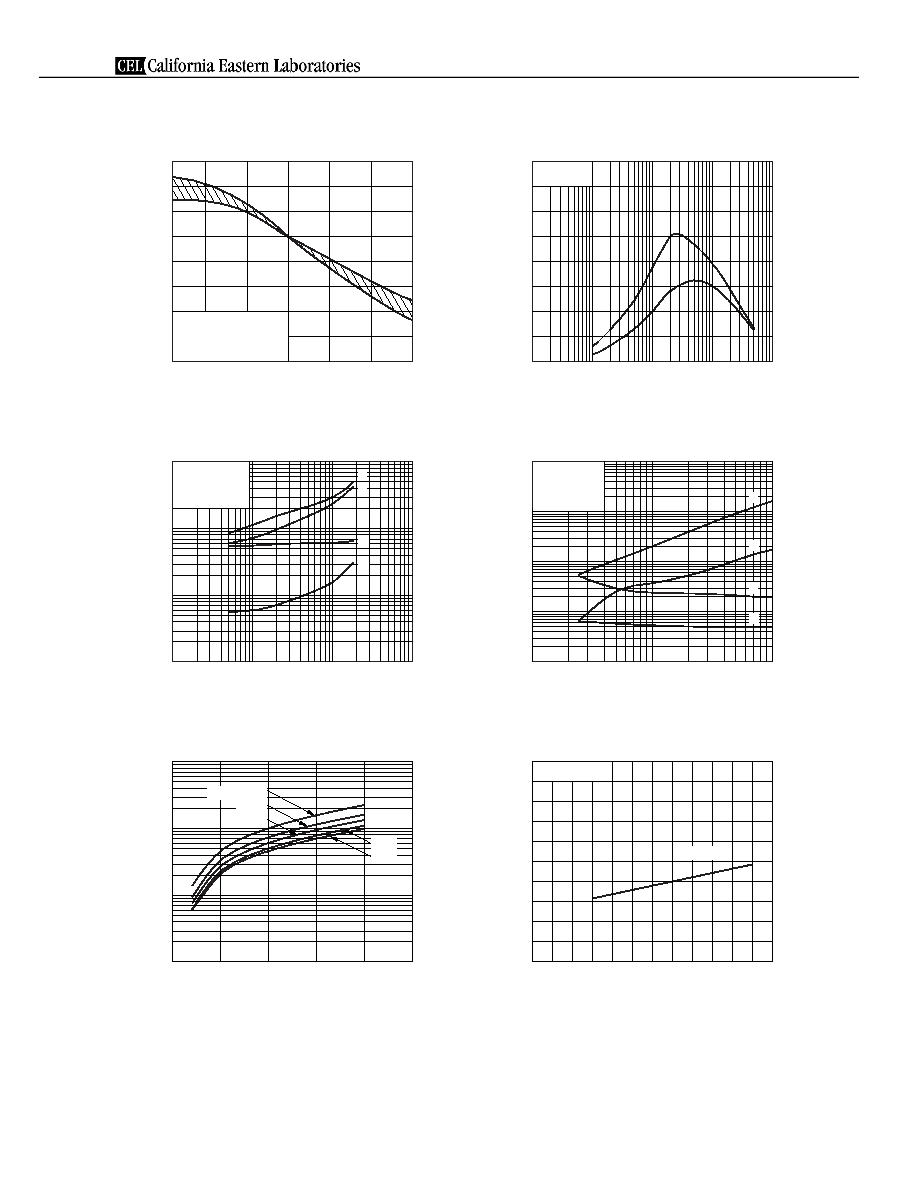
TYPICAL CHARACTERISTICS (Unless otherwise specified, T
A
= 25
∞
C)
Ambient Temperature T
A
(∞C)
Maximum Forward Current I
F
(mA)
MAXIMUM FORWARD CURRENT vs.
AMBIENT TEMPERATURE
40
20
30
10
0
25
50
75
100
0.2 mA/∞C
Ambient Temperature T
A
(∞C)
Transistor Power Dissipation P
C
(mW)
TRANSISTOR POWER DISSIPATION
vs. AMBIENT TEMPERATURE
25
50
75
100
125
70
50
60
20
30
40
10
0
0.4 mA/∞C
Forward Voltage V
F
(V)
Forward Current I
F
(mA)
FORWARD CURRENT vs.
FORWARD VOLTAGE
100
10
1
0.1
0.01
0.0
0.5
1.0
1.5
2.0
0∞C
≠25∞C
≠40∞C
T
A
= +100∞C
+60∞C
+25∞C
Ambient Temperature T
A
(∞C)
Collector to Emitter Dark Current I
CEO
(nA)
COLLECTOR TO EMITTER DARK
CURRENT vs. AMBIENT TEMPERATURE
≠25
0
25
50
75
100
1
10
100
1 000
10 000
V
CE
= 24 V
70 V
Collector to Emitter Voltage V
CE
(V)
Collector Current I
C
(mA)
COLLECTOR CURRENT vs.
COLLECTOR TO EMITTER VOLTAGE
6
8
4
5
7
9
3
2
1
10
0
20
16
12
8
4
18
14
10
6
2
5 mA
2 mA
1 mA
0.5 mA
I
F
= 10 mA
Collector Saturation Voltage V
CE(sat)
(V)
Collector Current I
C
(mA)
COLLECTOR CURRENT vs.
COLLECTOR SATURATION VOLTAGE
0.1
100
10
1
0.0
0.2
0.4
0.6
0.8
1.0
CTR = 160%
I
F
= 0.5 mA
1 mA
2 mA
10 mA
5 mA
Remark The graphs indicate nominal characteristics.
Data Sheet PN10202EJ03V0DS
5
PS2841-4A,PS2841-4B
Normalized to 1.0
at T
A
= 25∞C,
I
F
= 1 mA, V
CE
= 0.4 V
Ambient Temperature T
A
(∞C)
Normalized Current Transfer Ratio CTR
NORMALIZED CURRENT TRANSFER
RATIO vs. AMBIENT TEMPERATURE
1.6
1.0
1.2
1.4
0.8
0.6
0.4
0.2
0.0
≠40
≠25
0
25
50
75
100
Forward Current I
F
(mA)
Current Transfer Ratio CTR (%)
CURRENT TRANSFER RATIO vs.
FORWARD CURRENT
0.01
0.1
1
10
100
0
50
150
100
200
250
300
350
400
V
CE
= 0.4 V
Switching Time t ( s)
µ
Load Resistance R
L
(
)
SWITCHING TIME vs.
LOAD RESISTANCE
0.1
1
10
100
10
50 100
500 1 k
5 k 10 k
I
C
= 2 mA,
V
CC
= 5 V,
CTR = 160%
t
f
t
r
t
d
t
s
Switching Time t ( s)
µ
Load Resistance R
L
(
)
SWITCHING TIME vs.
LOAD RESISTANCE
1
1 000
100
10
10 000
1 k
5 k
10 k
50 k
100 k
I
F
= 1 mA,
V
CC
= 5 V,
CTR = 160%
t
f
t
r
t
d
t
s
vs. FORWARD CURRENT
OPTICAL LEAKAGE CURRENT
Forward Current I
F
(mA)
Optical Leakage Current I
L
(nA)
1 000
100
10
1
5
10
15
20
25
0
10 V
5 V
V
CE
= 70 V
40 V
24 V
vs. AMBIENT TEMPERATURE
OPTICAL LEAKAGE CURRENT
Ambient Temperature T
A
(∞C)
Optical Leakage Current I
L
(nA)
50
45
30
25
40
35
20
15
10
5
0
≠20 ≠10 0
10 20 30 40 50 60 70 80 90
≠30
V
CE
= 24 V
I
F
= 5 mA
Remark The graphs indicate nominal characteristics.
Data Sheet PN10202EJ03V0DS
6
PS2841-4A,PS2841-4B
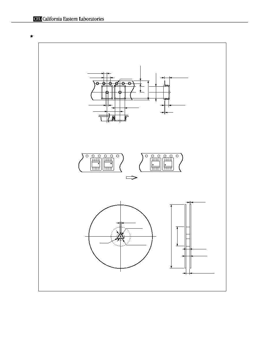
TAPING SPECIFICATIONS (UNIT: mm)
1.55±0.05
2.0±0.05
4.0±0.1
1.75±0.1
6.0±0.1
3.05 MAX.
7.4±0.1
0.3
8.0±0.1
1.5
+0.1
≠0
5.5±0.05
12.0±0.2
2.85±0.1
Tape Direction
Outline and Dimensions (Reel)
100±1.0
330±2.0
2.0±0.5
11.9 to 15.4
17.5±1.0
13.5±1.0
2.0±0.5
R 1.0
13.0±0.2
21.0±0.8
Outline and Dimensions (Tape)
Outer edge of
flange
Packing: 2 500 pcs/reel
PS2841-4A-F3
PS2841-4B-F3
PS2841-4A-F4
PS2841-4B-F4
Data Sheet PN10202EJ03V0DS
7
PS2841-4A,PS2841-4B
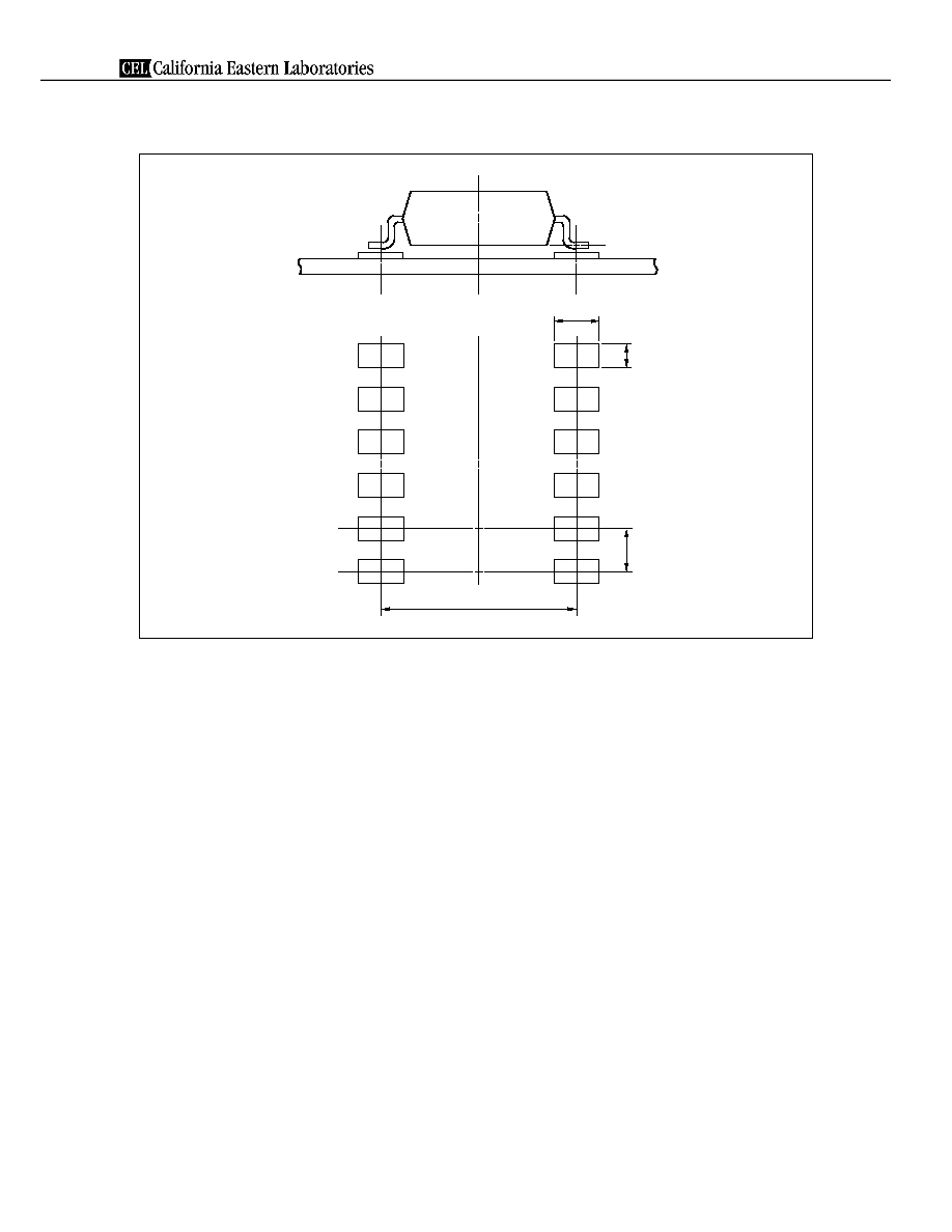
RECOMMENDED MOUNT PAD DIMENSIONS (UNIT: mm)
1.45
0.5
0.8
6.25
Data Sheet PN10202EJ03V0DS
8

PS2841-4A,PS2841-4B
NOTES ON HANDLING
1. Recommended soldering conditions
(1) Infrared reflow soldering
∑ Peak reflow temperature
260
∞
C or below (package surface temperature)
∑ Time of peak reflow temperature
10 seconds or less
∑ Time of temperature higher than 220
∞
C
60 seconds or less
∑ Time to preheat temperature from 120 to 180
∞
C 120
±
30 s
∑ Number of reflows
Three
∑ Flux
Rosin flux containing small amount of chlorine (The flux with a
maximum chlorine content of 0.2 Wt% is recommended.)
120±30 s
(preheating)
220∞C
180∞C
Package Surface Temperature T (∞C)
Time (s)
Recommended Temperature Profile of Infrared Reflow
(heating)
to 10 s
to 60 s
260∞C MAX.
120∞C
(2) Wave soldering
∑ Temperature
260
∞
C or below (molten solder temperature)
∑ Time
10 seconds or less
∑ Preheating conditions
120
∞
C or below (package surface temperature)
∑ Number of times
One (Allowed to be dipped in solder including plastic mold portion.)
∑ Flux
Rosin flux containing small amount of chlorine (The flux with a maximum chlorine
content of 0.2 Wt% is recommended.)
(3) Soldering by soldering iron
∑ Peak temperature (lead part temperature)
350
∞
C or below
∑ Time (each pins)
3 seconds or less
∑ Flux
Rosin flux containing small amount of chlorine (The flux with a
maximum chlorine content of 0.2 Wt% is recommended.)
(a) Soldering of leads should be made at the point 1.5 to 2.0 mm from the root of the lead.
(b) Please be sure that the temperature of the package would not be heated over 100
∞
C.
Data Sheet PN10202EJ03V0DS
9

PS2841-4A,PS2841-4B
(4) Cautions
∑ Fluxes
Avoid removing the residual flux with freon-based and chlorine-based cleaning solvent.
2. Cautions regarding noise
Be aware that when voltage is applied suddenly between the photocoupler's input and output or between
collector-emitters at startup, the output transistor may enter the on state, even if the voltage is within the absolute
maximum ratings.
USAGE CAUTIONS
1. Protect against static electricity when handling.
2. Avoid storage at a high temperature and high humidity.
Data Sheet PN10202EJ03V0DS
10
4590 Patrick Henry Drive
Santa Clara, CA 95054-1817
Telephone: (408) 919-2500
Facsimile: (408) 988-0279
Subject: Compliance with EU Directives
CEL certifies, to its knowledge, that semiconductor and laser products detailed below are compliant
with the requirements of European Union (EU) Directive 2002/95/EC Restriction on Use of Hazardous
Substances in electrical and electronic equipment (RoHS) and the requirements of EU Directive
2003/11/EC Restriction on Penta and Octa BDE.
CEL Pb-free products have the same base part number with a suffix added. The suffix ≠A indicates
that the device is Pb-free. The ≠AZ suffix is used to designate devices containing Pb which are
exempted from the requirement of RoHS directive (*). In all cases the devices have Pb-free terminals.
All devices with these suffixes meet the requirements of the RoHS directive.
This status is based on CEL's understanding of the EU Directives and knowledge of the materials that
go into its products as of the date of disclosure of this information.
Restricted Substance
per RoHS
Concentration Limit per RoHS
(values are not yet fixed)
Concentration contained
in CEL devices
-A -AZ
Lead (Pb)
< 1000 PPM
Not Detected
(*)
Mercury
< 1000 PPM
Not Detected
Cadmium
< 100 PPM
Not Detected
Hexavalent Chromium
< 1000 PPM
Not Detected
PBB
< 1000 PPM
Not Detected
PBDE
< 1000 PPM
Not Detected
If you should have any additional questions regarding our devices and compliance to environmental
standards, please do not hesitate to contact your local representative.
Important Information and Disclaimer: Information provided by CEL on its website or in other communications concerting the substance
content of its products represents knowledge and belief as of the date that it is provided. CEL bases its knowledge and belief on information
provided by third parties and makes no representation or warranty as to the accuracy of such information. Efforts are underway to better
integrate information from third parties. CEL has taken and continues to take reasonable steps to provide representative and accurate
information but may not have conducted destructive testing or chemical analysis on incoming materials and chemicals. CEL and CEL
suppliers consider certain information to be proprietary, and thus CAS numbers and other limited information may not be available for
release.
In no event shall CEL's liability arising out of such information exceed the total purchase price of the CEL part(s) at issue sold by CEL to
customer on an annual basis.
See CEL Terms and Conditions for additional clarification of warranties and liability.