 | –≠–ª–µ–∫—Ç—Ä–æ–Ω–Ω—ã–π –∫–æ–º–ø–æ–Ω–µ–Ω—Ç: PS9851-1 | –°–∫–∞—á–∞—Ç—å:  PDF PDF  ZIP ZIP |

PRELIMINARY DATA SHEET
The information in this document is subject to change without notice. Before using this document, please confirm that
this is the latest version.
Not all devices/types available in every country. Please check with local NEC Compound Semiconductor Devices
representative for availability and additional information.
PHOTOCOUPLER
PS9851-1,-2
Document No. PN10493EJ01V0DS (1st edition)
Date Published May 2004 CP(K)
Printed in Japan
NEC Compound Semiconductor Devices 2004
HIGH NOISE REDUCTION, 15 Mbps CMOS OUTPUT TYPE
8-PIN SSOP PHOTOCOUPLER
-NEPOC Series-
1. Anode1
2. Cathode1
3. Cathode2
4. Anode2
5. GND
6. V
O
2
7. V
O
1
8. V
DD
1. NC
2. Anode
3. Cathode
4. NC
5. GND
6. V
O
7. NC
8. V
DD
1
2
3
4
8
7
6
5
SHIELD
PIN CONNECTION
(Top View)
PS9851-2
PS9851-1
SHIELD
1
2
3
4
8
7
6
5
DESCRIPTION
The PS9851-1, -2 are optically coupled isolators containing GaAlAs LED on the input side and a CMOS output IC
on the output side.
They are high common mode transient immunity (CMR), high-speed CMOS output type photocouplers designed for
high-speed logic interface circuits.
FEATURES
∑ High-speed response (15 Mbps)
∑ Operable at high temperature (
-40 to +100∞C)
∑ High common mode transient immunity (CM
H
, CM
L
=
±15 kV/
µ
s TYP.)
∑ High isolation voltage (BV = 2 500 Vr.m.s.)
∑ Pulse width distortion (
t
PHL
-t
PLH
= 5 ns TYP.)
∑ Ordering number of tape product : PS9851-1-F3, F4: 1 500 pcs/reel
: PS9851-2-F3, F4: 1 500 pcs/reel
∑ Safety
standards
∑ UL awaiting approved
∑ DIN EN60747-5-2 (VDE0884 Part2) awaiting approved
APPLICATIONS
∑ FA
Network
∑ Measurement
equipment
∑ PDP

Preliminary Data Sheet PN10493EJ01V0DS
2
PS9851-1,-2
PACKAGE DIMENSIONS (UNIT: mm)
1.27
0.4
+0.10
≠0.05
0.25 M
0.1±0.1
3.95±0.1
6.0±0.2
0.5±0.3
0.15
+0.10 ≠0.05
3.27±0.2
0.10 S
5.08±0.15
5.21±0.25 (include burr)
MARKING EXAMPLE
PS9851-1
PS9851-2
4 51
Week Assembled
Year Assembled
(Last 1 Digit)
No. 1 pin Mark
Initial of NEC
(Engraved mark)
Assembly Lot
*1
N
9851-2
N451
N
Rank Code
*1 For the external plating Sn-Bi product,
L is indicated at the second digit of the rank.
4 51
Week Assembled
Year Assembled
(Last 1 Digit)
No. 1 pin Mark
Initial of NEC
(Engraved mark)
N
Rank Code
*1 For the external plating Sn-Bi product,
L is indicated at the second digit of the rank.
Assembly Lot
*1
N
9851-1
N451
Type Number
Type Number
Preliminary Data Sheet PN10493EJ01V0DS
3
PS9851-1,-2
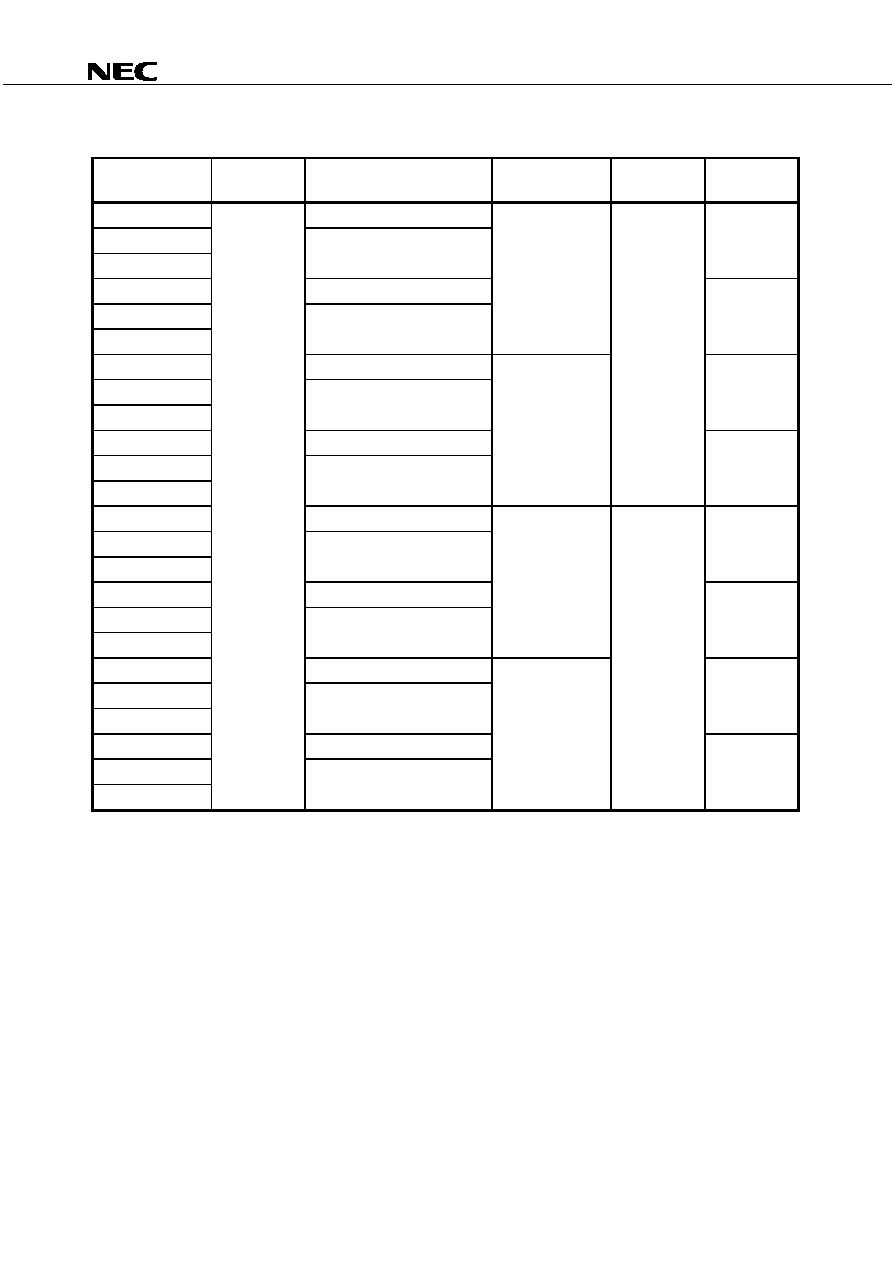
ORDERING INFORMATION
Part Number
Package
Packing Style
Safety Standards
Approval
Solder plating
specification
Application
Part Number
*1
PS9851-1
8-pin SSOP
20 pcs (Tape 20 pcs cut) Standard
products
Sn-Pb PS9851-1
PS9851-1-F3
(SO-8)
Embossed Tape 1 500 pcs/reel
(UL awaiting
PS9851-1-F4
approved)
PS9851-2
20 pcs (Tape 20 pcs cut)
PS9851-2
PS9851-2-F3
Embossed Tape 1 500 pcs/reel
PS9851-2-F4
PS9851-1-V
20 pcs (Tape 20 pcs cut)
DIN EN60747-5-2
PS9851-1
PS9851-1-V-F3
Embossed Tape 1 500 pcs/reel
(VDE0884 Part2)
PS9851-1-V-F4
awaiting approved
PS9851-2-V
20 pcs (Tape 20 pcs cut)
(Option)
PS9851-2
PS9851-2-V-F3
Embossed Tape 1 500 pcs/reel
PS9851-2-V-F4
PS9851-1-A
20 pcs (Tape 20 pcs cut) Standard
products
Sn-Bi PS9851-1
PS9851-1-F3-A
Embossed Tape 1 500 pcs/reel
(UL awaiting
PS9851-1-F4-A
approved)
PS9851-2-A
20 pcs (Tape 20 pcs cut)
PS9851-2
PS9851-2-F3-A
Embossed Tape 1 500 pcs/reel
PS9851-2-F4-A
PS9851-1-V-A
20 pcs (Tape 20 pcs cut)
DIN EN60747-5-2
PS9851-1
PS9851-1-V-F3-A
Embossed Tape 1 500 pcs/reel
(VDE0884 Part2)
PS9851-1-V-F4-A
awaiting approved
PS9851-2-V-A
20 pcs (Tape 20 pcs cut)
(Option)
PS9851-2
PS9851-2-V-F3-A
Embossed Tape 1 500 pcs/reel
PS9851-2-V-F4-A
*1 For the application of the Safety Standard, following part number should be used.

Preliminary Data Sheet PN10493EJ01V0DS
4
PS9851-1,-2
ABSOLUTE MAXIMUM RATINGS (T
A
= 25
∞C, unless otherwise specified)
Parameter Symbol
Ratings
Unit
Forward Current
I
F
20 mA
Diode
Reverse Voltage
V
R
5 V
Supply Voltage
V
DD
0 to 5.5
V
Output Voltage
V
O
-0.5 to V
DD
+0.5 V
Detector
Output Current
I
O
2 mA
Isolation Voltage
*1
BV
2
500
Vr.m.s.
Operating Ambient Temperature
T
A
-40 to +100
∞C
Storage Temperature
T
stg
-55 to +125
∞C
*1 AC voltage for 1 minute at T
A
= 25
∞C, RH = 60% between input and output.
RECOMMENDED OPERATING CONDITIONS (T
A
= 25
∞C)
Parameter Symbol
MIN.
TYP.
MAX.
Unit
Forward Current
I
F
10 16
mA
Supply Voltage
V
DD
4.5 5.0 5.5 V

Preliminary Data Sheet PN10493EJ01V0DS
5
PS9851-1,-2
ELECTRICAL CHARACTERISTICS (T
A
=
-40 to +100∞C, V
DD
= 4.5 to 5.5 V, unless otherwise
specified)
Parameter Symbol
Conditions
MIN.
TYP.
*1
MAX. Unit
Forward Voltage
V
F
I
F
= 10 mA, T
A
= 25
∞C
1.6
1.9
V
Reverse Current
I
R
V
R
= 3 V, T
A
= 25
∞C
10
µ
A
Diode
Terminal Capacitance
C
t
V = 0 V, f = 1 MHz, T
A
= 25
∞C 30 pF
High Level Supply Current
I
DDH
I
F
= 0 mA (1ch)
3
5
Low Level Supply Current
I
DDL
I
F
= 10 mA (1ch)
3
5
mA
High Level Output Voltage
V
OH
I
O
=
-20
µ
A, I
F
= 0 mA
4.0
5.0
Detector
Low Level Output Voltage
V
OL
I
O
= 20
µ
A, I
F
= 10 mA
0.01
0.1
V
Threshold Input Current
I
FHL
V
O
< 1 V
6
mA
Isolation Resistance
R
I
-
O
V
I-O
= 1 kV
DC
, RH = 40 to 60%,
T
A
= 25
∞C
10
11
Isolation Capacitance
C
I-O
V = 0 V, f = 1 MHz, T
A
= 25
∞C
0.9 pF
Propagation Delay Time
(H
L)
*2
t
PHL
35
60
Propagation Delay Time
(L
H)
*2
t
PLH
30
60
Pulse Width
PW
100
Pulse Width Distortion
(PWD)
t
PHL
-t
PLH
5
30
Propagation Delay Skew
t
PSK
40
Rise Time
t
r
3
Fall Time
t
f
I
F
= 10 mA, V
DD
= 5 V,
CL = 15 pF, CMOS Levels
3
ns
Common Mode
Transient Immunity at
High Level Output
*3
CM
H
V
DD
= 5 V, I
F
= 0 mA,
V
CM
= 1 kV, V
O
> 4 V, T
A
= 25
∞C
10 15
Coupled
Common Mode
Transient Immunity at
Low Level Output
*3
CM
L
V
DD
= 5 V, I
F
= 10 mA,
V
CM
= 1 kV, V
O
< 1 V, T
A
= 25
∞C
10 15
kV/
µ
s
*1 Typical values at T
A
= 25
∞C