 | –≠–ª–µ–∫—Ç—Ä–æ–Ω–Ω—ã–π –∫–æ–º–ø–æ–Ω–µ–Ω—Ç: XD1002 | –°–∫–∞—á–∞—Ç—å:  PDF PDF  ZIP ZIP |
Mimix Broadband
's 0.05-50.0 GHz GaAs MMIC
distributed amplifier has a small signal gain of 9.0 dB
with a noise figure of 5.0 dB across the band. The
device also includes 15.0 dB gain control and a +9.0
dBm P1dB compression point. This MMIC uses Mimix
Broadband
's 0.15 µm GaAs PHEMT device model
technology, and is based upon electron beam
lithography to ensure high repeatability and
uniformity. The chip has surface passivation to protect
and provide a rugged part with backside via holes and
gold metallization to allow either a conductive epoxy
or eutectic solder die attach process. This device is well
suited for microwave, millimeter-wave, wideband
military, and fiber optic applications.
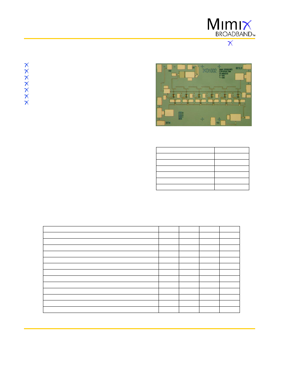
0.05-50.0 GHz GaAs MMIC
Distributed Amplifier
Absolute Maximum Ratings
Page 1 of 6
Features
Wide Band Driver Amplifier
9.0 dB Small Signal Gain
5.0 dB Noise Figure
15.0 dB Gain Control
+9.0 dBm P1dB Compression Point
100% On-Wafer RF, DC and Output Power Testing
100% Visual Inspection to MIL-STD-883
Method 2010
General Description
Supply Voltage (Vd)
Supply Current (Id)
Gate Bias Voltage (Vg)
Input Power (Pin)
Storage Temperature (Tstg)
Operating Temperature (Ta)
Channel Temperature (Tch)
+10.0 VDC
150 mA
+0.3 VDC
+18 dBm
-65 to +165
O
C
-55 to MTTF Table
MTTF Table
Chip Device Layout
(2) Channel temperature affects a device's MTTF. It is
recommended to keep channel temperature as low as
possible for maximum life.
2
Frequency Range (f )
Input Return Loss (S11)
Output Return Loss (S22)
Small Signal Gain (S21)
Gain Flatness (
S21)
Gain Control
Reverse Isolation (S12)
Noise Figure (NF)
Output Power for 1 dB Compression (P1dB)
Drain Bias Voltage (Vd)
Gain Control Bias (Vg1)
Gate Bias Voltage (Vg2)
Supply Current (Id) (Vd=8.5V, Vg1=0.0V, Vg2=1.0V Typical)
Electrical Characteristics (Ambient Temperature T = 25
o
C)
Parameter
Units
GHz
dB
dB
dB
dB
dB
dB
dB
dBm
VDC
VDC
VDC
mA
Min.
0.05
-
-
-
-
-
-
-
-
-
-2.0
-
-
Typ.
-
14.0
14.0
9.0
+/-1.5
15.0
40.0
5.0
+9.0
+8.5
0.0
+1.0
120
Max.
50.0
-
-
-
-
-
-
-
-
+9.0
0.1
-
140
(1) Measured using constant current.
1
2
Mimix Broadband, Inc., 10795 Rockley Rd., Houston, Texas 77099
Tel: 281.988.4600 Fax: 281.988.4615 mimixbroadband.com
Characteristic Data and Specifications are subject to change without notice.
©2005 Mimix Broadband, Inc.
Export of this item may require appropriate export licensing from the U.S. Government. In purchasing these parts, U.S. Domestic customers accept
their obligation to be compliant with U.S. Export Laws.
D1002
August 2005 - Rev 04-Aug-05
Page 2 of 6
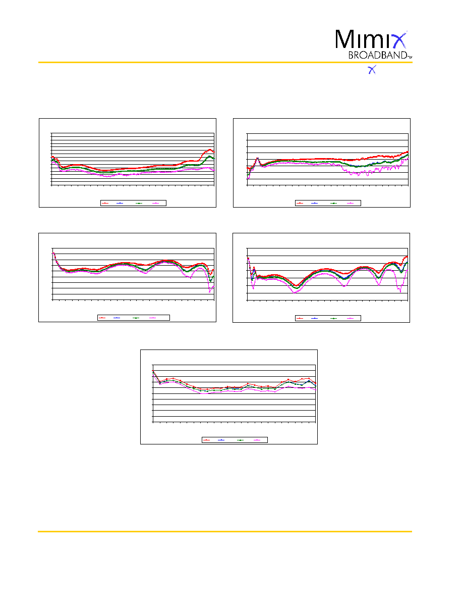
Distributed Amplifier Measurements
Mimix Broadband, Inc., 10795 Rockley Rd., Houston, Texas 77099
Tel: 281.988.4600 Fax: 281.988.4615 mimixbroadband.com
Characteristic Data and Specifications are subject to change without notice.
©2005 Mimix Broadband, Inc.
Export of this item may require appropriate export licensing from the U.S. Government. In purchasing these parts, U.S. Domestic customers accept
their obligation to be compliant with U.S. Export Laws.
0.05-50.0 GHz GaAs MMIC
Distributed Amplifier
D1002
XD1002 Vd=8.5 V Id=120 mA
~70 Devices
5
6
7
8
9
10
11
12
13
14
15
16
17
18
19
20
2
4
6
8
10
12
14
16
18
20
22
24
26
28
30
32
34
36
38
40
42
44
46
48
50
Fre que ncy (GHz )
G
a
in
(
d
B
)
Max
Median
Mean
Min
0.05
XD1002 Vd=8.5 V Id=120 mA
~70 Devices
-80
-70
-60
-50
-40
-30
-20
-10
0
2
4
6
8
10
12
14
16
18
20
22
24
26
28
30
32
34
36
38
40
42
44
46
48
50
Fre que ncy (GHz )
R
e
ve
r
s
e I
s
o
l
at
i
o
n
(
d
B
)
Max
Median
Mean
Min
0.05
XD1002 Vd=8.5 V Id=120 mA
~70 Devices
-45
-40
-35
-30
-25
-20
-15
-10
-5
0
2
4
6
8
10
12
14
16
18
20
22
24
26
28
30
32
34
36
38
40
42
44
46
48
50
Fre que ncy (GHz )
I
n
p
u
t Re
tu
r
n
L
o
ss
(d
B
)
Max
Median
Mean
-3sigma
0.05
XD1002 Vd=8.5 V Id=120 mA
~70 Devices
-35
-30
-25
-20
-15
-10
-5
0
2
4
6
8
10
12
14
16
18
20
22
24
26
28
30
32
34
36
38
40
42
44
46
48
50
Fre que ncy (GHz )
O
u
tp
u
t
Re
tu
r
n
L
o
ss
(
d
B)
Max
Median
Mean
Min
0.05
XD1002 Vd=8.5 V Id=120 mA
~30 Devices
3
4
5
6
7
8
9
10
11
12
13
2
4
6
8
10
12
14
16
18
20
22
24
26
28
30
32
34
36
38
40
42
44
46
48
50
Fre que ncy (GHz )
O
u
t
p
u
t
Po
w
e
r
P1
d
B
(
d
B
m
)
Max
Median
Mean
Min
August 2005 - Rev 04-Aug-05

Page 3 of 6
Distributed Amplifier Measurements (cont.)
Mimix Broadband, Inc., 10795 Rockley Rd., Houston, Texas 77099
Tel: 281.988.4600 Fax: 281.988.4615 mimixbroadband.com
Characteristic Data and Specifications are subject to change without notice.
©2005 Mimix Broadband, Inc.
Export of this item may require appropriate export licensing from the U.S. Government. In purchasing these parts, U.S. Domestic customers accept
their obligation to be compliant with U.S. Export Laws.
0.05-50.0 GHz GaAs MMIC
Distributed Amplifier
D1002
0
5
10
15
20
25
30
35
40
45
50
55
60
65
70
Frequency (GHz)
Sparams
-30
-28
-26
-24
-22
-20
-18
-16
-14
-12
-10
-8
-6
-4
-2
0
2
4
6
8
10
12
14
16
S11
S21
S22
Nois e Figure & Ga in from 3 sam ples; Vd=8.5V, Id=120mA, Vg1=0V, Vg2=1V
0
1
2
3
4
5
6
7
8
9
10
11
12
18
20
22
24
26
28
30
32
34
36
38
40
42
Freque ncy ( GHz)
No
i
s
e
F
i
g
u
re
& G
a
i
n
(
d
B)
August 2005 - Rev 04-Aug-05
Page 4 of 6
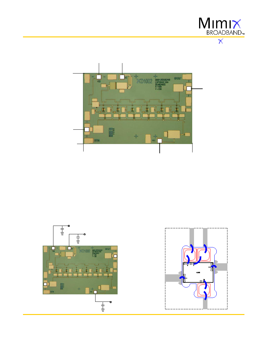
Mechanical Drawing
Bond Pad #1 (RF In)
Bond Pad #2 (Vg2)
Bond Pad #3 (Vd)
Bond Pad #4 (RF Out)
Bond Pad #5 (Vg1)
Bias Arrangement
Bypass Capacitors - See App Note [2]
Mimix Broadband, Inc., 10795 Rockley Rd., Houston, Texas 77099
Tel: 281.988.4600 Fax: 281.988.4615 mimixbroadband.com
Characteristic Data and Specifications are subject to change without notice.
©2005 Mimix Broadband, Inc.
Export of this item may require appropriate export licensing from the U.S. Government. In purchasing these parts, U.S. Domestic customers accept
their obligation to be compliant with U.S. Export Laws.
0.05-50.0 GHz GaAs MMIC
Distributed Amplifier
D1002
(Note: Engineering designator is 25LN6DA0522)
Units: millimeters (inches) Bond pad dimensions are shown to center of bond pad.
Thickness: 0.110 +/- 0.010 (0.0043 +/- 0.0004), Backside is ground, Bond Pad/Backside Metallization: Gold
All DC Bond Pads are 0.100 x 0.100 (0.004 x 0.004). All RF Bond Pads are 0.100 x 0.200 (0.004 x 0.008)
Bond pad centers are approximately 0.109 (0.004) from the edge of the chip.
Dicing tolerance: +/- 0.005 (+/- 0.0002). Approximate weight: 1.417 mg.
1
2
4
5
3
Vg2
RF In
RF Out
Vd
Vg1
1
2
4
5
1.300
(0.051)
0.295
(0.012)
1.950
(0.077)
0.0
0.0
0.295
(0.012)
3
0.695
(0.027)
1.005
(0.040)
1.360
(0.054)
RF Out
Vg1
RF In
Vd
Vg2
August 2005 - Rev 04-Aug-05
Page 5 of 6
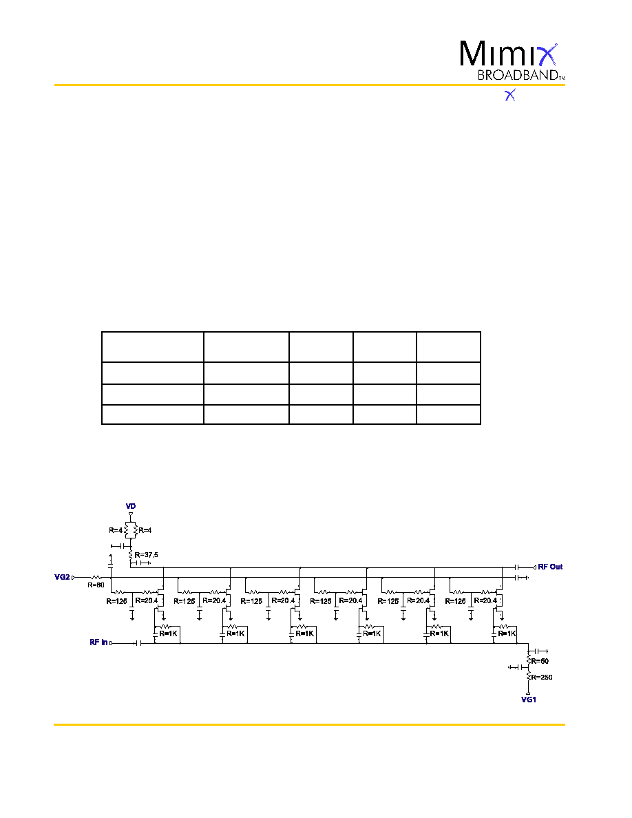
Device Schematic
App Note [1] Biasing
- As shown in the bonding diagram, this device is operated with a single drain and gate
voltage and it also includes a separate gain control voltage. Maximum gain bias is nominally Vd=8.5V, Vg1=0.0V,
Vg2=1.0V, and Id=120mA. Gain can be adjusted by changing Vg1. It is recommended to use active biasing to keep the
currents constant as the RF power and temperature vary; this gives the most reproducible results. Depending on the
supply voltage available and the power dissipation constraints, the bias circuit may be a single transistor or a low power
operational amplifier, with a low value resistor in series with the drain supply used to sense the current. The gate of the
pHEMT is controlled to maintain correct drain current and thus drain voltage. The typical gate voltage needed to do this
is 0.0V. Typically the gate is protected with Silicon diodes to limit the applied voltage. Also, make sure to sequence the
applied voltage to ensure negative gate bias is available before applying the positive drain supply.
App Note [2] Bias Arrangement
- Each DC pad (Vd and Vg1,2) need to have DC bypass capacitance (~100-200 pF) as
close to the device as possible. Additional DC bypass capacitance (~0.01 uF) is also recommended.
Mimix Broadband, Inc., 10795 Rockley Rd., Houston, Texas 77099
Tel: 281.988.4600 Fax: 281.988.4615 mimixbroadband.com
Characteristic Data and Specifications are subject to change without notice.
©2005 Mimix Broadband, Inc.
Export of this item may require appropriate export licensing from the U.S. Government. In purchasing these parts, U.S. Domestic customers accept
their obligation to be compliant with U.S. Export Laws.
0.05-50.0 GHz GaAs MMIC
Distributed Amplifier
D1002
MTTF Table (TBD)
Backplate
Temperature
55 deg Celsius
75 deg Celsius
95 deg Celsius
Channel
Temperature
deg Celsius
deg Celsius
deg Celsius
FITs
E+
E+
E+
MTTF Hours
E+
E+
E+
Rth
C/W
C/W
C/W
Bias Conditions: Vd=8.5V, Id=120 mA
These numbers were calculated based on accelerated life test information and thermal model analysis received from the fabricating foundry.
August 2005 - Rev 04-Aug-05