 | –≠–ª–µ–∫—Ç—Ä–æ–Ω–Ω—ã–π –∫–æ–º–ø–æ–Ω–µ–Ω—Ç: XP1001 | –°–∫–∞—á–∞—Ç—å:  PDF PDF  ZIP ZIP |
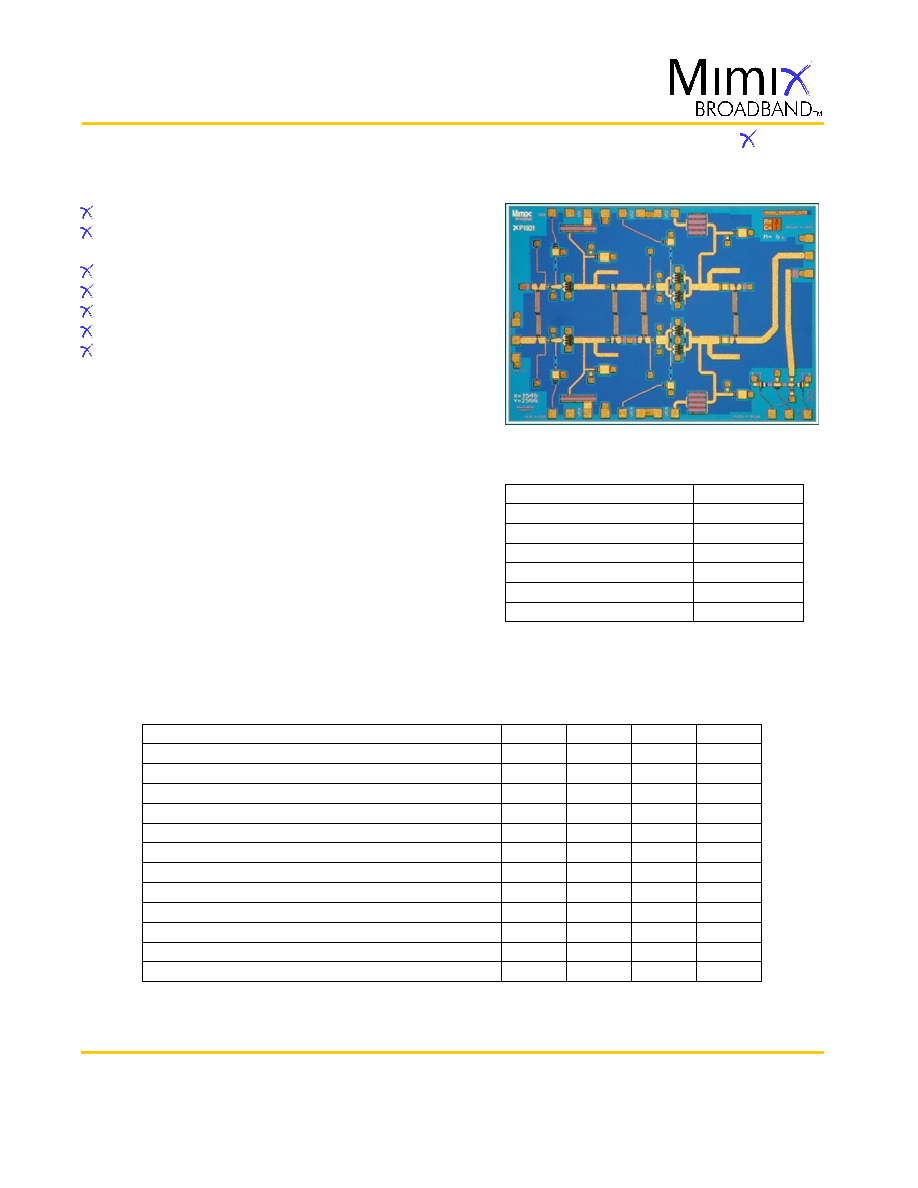
Chip Device Layout
High Linearity Wideband Amplifier
On-Chip Temperature Compensated
Output Power Detector
Balanced Design Provides Good Input/Output Match
11.0 dB Small Signal Gain
+31.0 dBm Third Order Intercept (OIP3)
100% On-Wafer RF, DC and Output Power Testing
100% Visual Inspection to MIL-STD-883
Method 2010
General Description
Mimix Broadband
's two stage 26.0-40.0 GHz GaAs MMIC
power amplifier is optimized for linear operation with a third
order intercept point of +31.0 dBm. The device also includes
Lange couplers to achieve good input/output return loss
and an on-chip temperature compensated output power
detector. This MMIC uses Mimix Broadband
's 0.15 µm GaAs
PHEMT device model technology, and is based upon
electron beam lithography to ensure high repeatability and
uniformity. The chip has surface passivation to protect and
provide a rugged part with backside via holes and gold
metallization to allow either a conductive epoxy or eutectic
solder die attach process. This device is well suited for
Millimeter-wave Point-to-Point Radio, LMDS, SATCOM and
VSAT applications.
26.0-40.0 GHz GaAs MMIC
Power Amplifier
Units
GHz
dB
dB
dB
dB
dB
dBm
dBm
Vdc
Vdc
mA
Vdc
Min.
26.0
-
-
-
-
-
-
-
-
-1.0
-
-
Typ.
-
18.0
18.0
11.0
+/-1.0
40.0
+21.0
+31.0
5.5
-0.5
430
0.28
Max.
40.0
-
-
-
-
-
-
-
5.6
0.0
650
-
Parameter
Frequency Range (f )
Input Return Loss (S11)
Output Return Loss (S22)
Small Signal Gain (S21)
Gain Flatness (
S21)
Reverse Isolation (S12)
Output Power for 1dB Compression (P1dB)
Output Third Order Intercept Point (OIP3)
Drain Bias Voltage (Vd1,2,3,4) (Vd5 [Det], Rd=3-6K )
Gate Bias Voltage (Vg1,2,3,4)
Supply Current (Id) (Vd=5.5V, Vg=-0.5V Typical)
Detector (diff ) Output at 20dBm
Electrical Characteristics (Ambient Temperature T=25
o
C)
Page 1 of 6
Features
(1) Measured at +17 dBm per tone output carrier level across the full frequency band.
(2) Measured using constant current.
(3) Measured with either Vd5=I.0V, or Vd5=5.5V and Rd=5.6K
.
+6.0 Vdc
700 mA
+0.3 Vdc
+14.0 dBm
-65 to +165
O
C
-55 to MTTF Table
MTTF Table
Supply Voltage (Vd)
Supply Current (Id)
Gate Bias Voltage (Vg)
Input Power (Pin)
Storage Temperature (Tstg)
Operating Temperature (Ta)
Channel Temperature (Tch)
Absolute Maximum Ratings
4
(4) Channel temperature affects a device's MTTF. It is
recommended to keep channel temperature as low as
possible for maximum life.
2
1,2
3
Mimix Broadband, Inc., 10795 Rockley Rd., Houston, Texas 77099
Tel: 281.988.4600 Fax: 281.988.4615 mimixbroadband.com
Characteristic Data and Specifications are subject to change without notice.
©2004 Mimix Broadband, Inc.
Export of this item may require appropriate export licensing from the U.S. Government. In purchasing these parts, U.S. Domestic customers accept
their obligation to be compliant with U.S. Export Laws.
4
May 2005 - Rev 05-May-05
P1001
26.0-40.0 GHz GaAs MMIC
Power Amplifier
Page 2 of 6
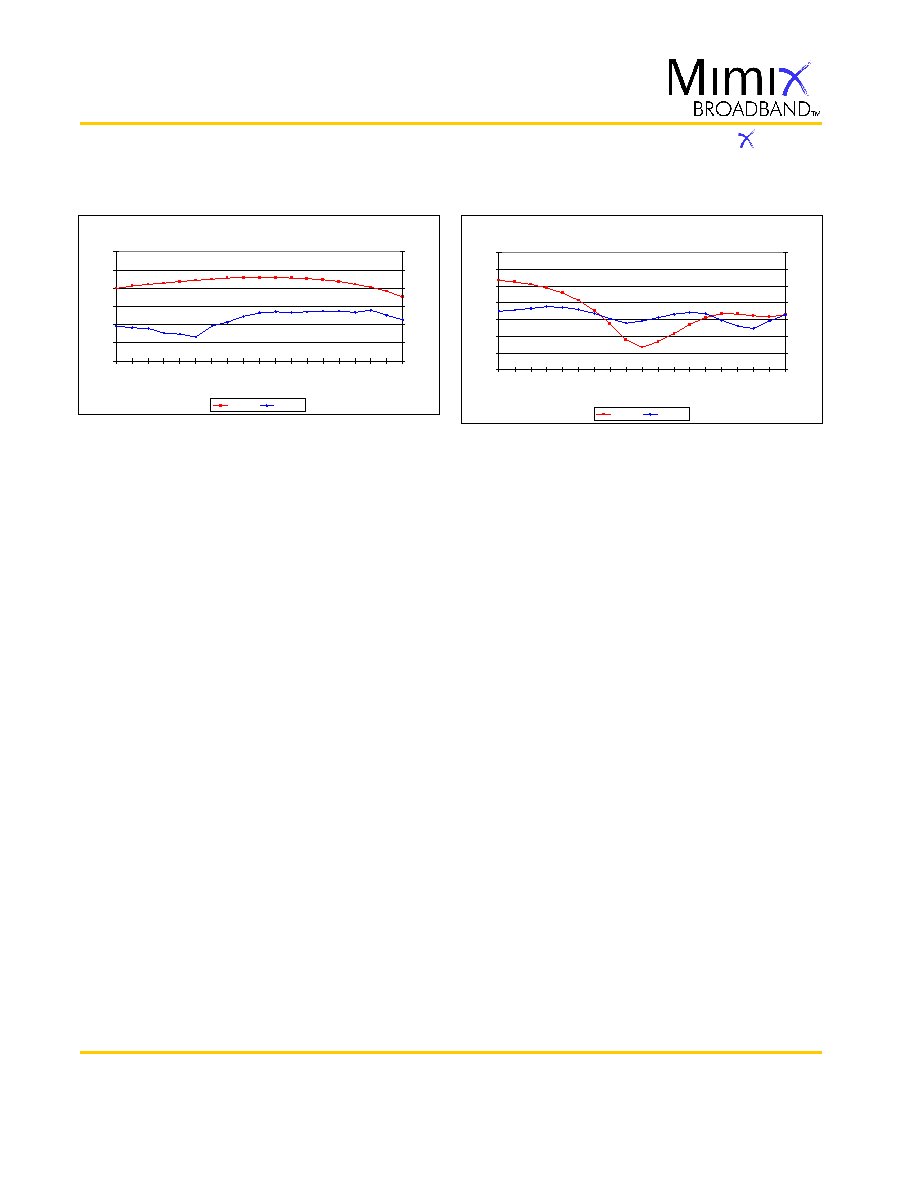
Power Amplifier Measurements
XP1001 Vd1,2,3,4=5.5 V Id1,2,3,4=430 mA
-35
-30
-25
-20
-15
-10
-5
0
24.0
26.0
28.0
30.0
32.0
34.0
36.0
38.0
40.0
42.0
Frequency (GHz)
In
p
u
t
R
e
t
u
r
n
L
o
s
s
(
d
B
)
-35
-30
-25
-20
-15
-10
-5
0
O
u
tp
u
t
R
e
tu
r
n
L
o
s
s
(d
B
)
S11 Avg
S22 Avg
XP1001 Vd1,2,3,4=5.5 V Id1,2,3,4=430 mA
-10
-5
0
5
10
15
20
24.0
26.0
28.0
30.0
32.0
34.0
36.0
38.0
40.0
42.0
Frequency (GHz)
G
a
in
(
d
B
)
-70
-60
-50
-40
-30
-20
-10
R
eve
r
s
e I
s
o
l
at
i
o
n
(
d
B
)
S21 Avg
S12 Avg
Mimix Broadband, Inc., 10795 Rockley Rd., Houston, Texas 77099
Tel: 281.988.4600 Fax: 281.988.4615 mimixbroadband.com
Characteristic Data and Specifications are subject to change without notice.
©2004 Mimix Broadband, Inc.
Export of this item may require appropriate export licensing from the U.S. Government. In purchasing these parts, U.S. Domestic customers accept
their obligation to be compliant with U.S. Export Laws.
P1001
May 2005 - Rev 05-May-05
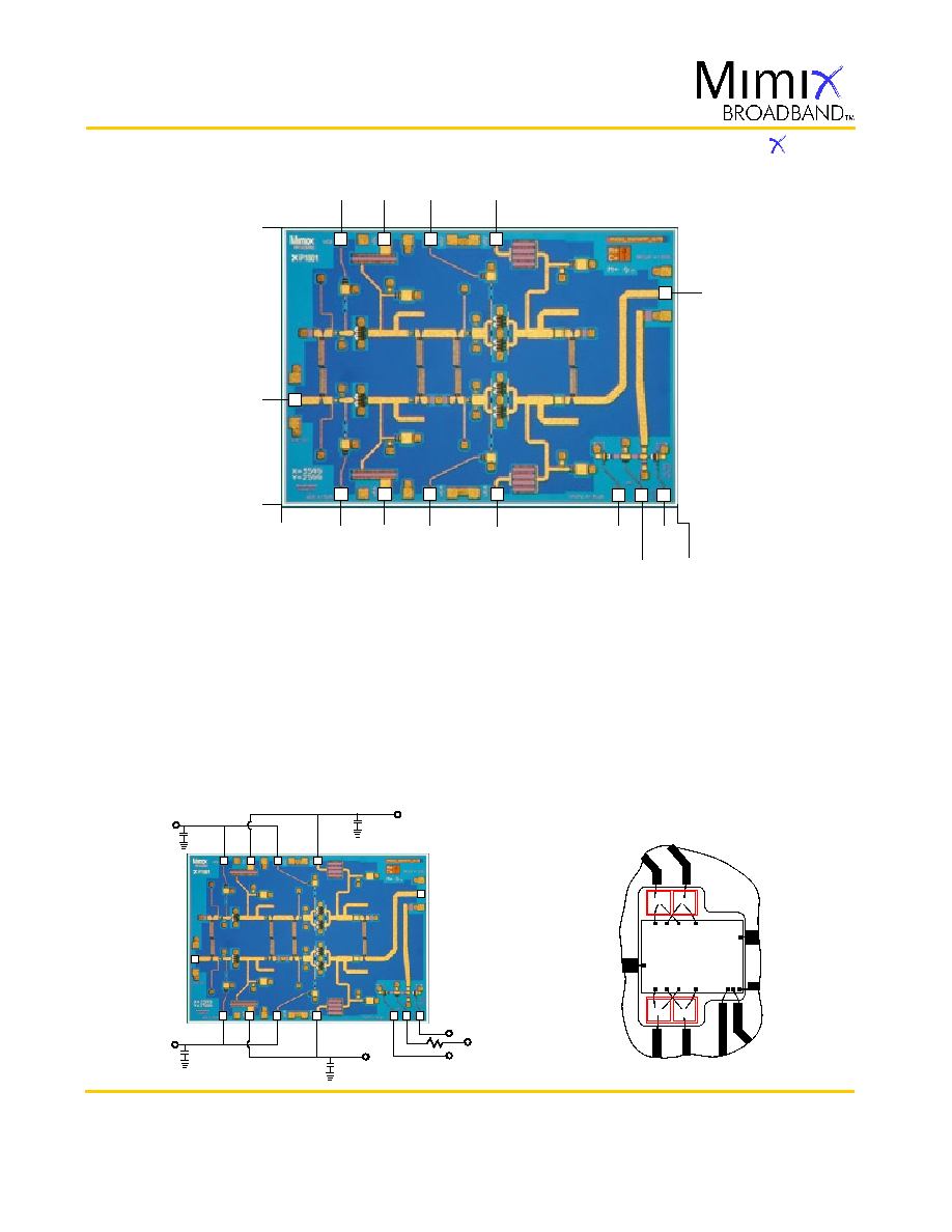
Mechanical Drawing
26.0-40.0 GHz GaAs MMIC
Power Amplifier
Bias Arrangement
(Note: Engineering designator is 38PAMP_07B)
Units: millimeters (inches) Bond pad dimensions are shown to center of bond pad.
Thickness: 0.110 +/- 0.010 (0.0043 +/- 0.0004), Backside is ground, Bond Pad/Backside Metallization: Gold
All Bond Pads are 0.100 x 0.100 (0.004 x 0.004).
Bond pad centers are approximately 0.109 (0.004) from the edge of the chip.
Dicing tolerance: +/- 0.005 (+/- 0.0002). Approximate weight: 5.482 mg.
Bond Pad #1 (RF In)
Bond Pad #2 (Vg1)
Bond Pad #3 (Vd1)
Bond Pad #4 (Vg2)
Bond Pad #5 (Vd2)
Bond Pad #6 (RF Out)
Bond Pad #7 (V2 Out)
Bond Pad #8 (Vd5)
Bond Pad #9 (V1 Out)
Bond Pad #10 (Vd4)
Bond Pad #11 (Vg4)
Bond Pad #12 (Vd3)
Bond Pad #13 (Vg3)
Page 3 of 6
Bypass Capacitors - See App Note [3]
Mimix Broadband, Inc., 10795 Rockley Rd., Houston, Texas 77099
Tel: 281.988.4600 Fax: 281.988.4615 mimixbroadband.com
Characteristic Data and Specifications are subject to change without notice.
©2004 Mimix Broadband, Inc.
Export of this item may require appropriate export licensing from the U.S. Government. In purchasing these parts, U.S. Domestic customers accept
their obligation to be compliant with U.S. Export Laws.
P1001
RF In
RF Out
Vg1,2
Vd1,2
Vg3,4 Vd3,4 V1 Out
Vd5
V2 Out
XP1001
2.500
(0.098)
1
2
3
4
5
6
7
8
9
10
11
12
13
0.516
(0.020)
0.914
(0.036)
1.313
(0.052)
1.915
(0.075)
1.910
(0.075)
3.540
(0.139)
3.414
(0.134)
3.213
(0.127)
3.012
(0.119)
1.915
(0.075)
1.313
(0.052)
0.914
(0.036)
0.516
(0.020)
0.0
0.0
0.945
(0.037)
1
2
3
4
5
6
7
8
9
10
11
12
13
Vg1,2
Vd1,2
RF Out
RF In
Vg3,4
Vd3,4
V2 Out
Rd
Vd5
V1 Out
May 2005 - Rev 05-May-05
26.0-40.0 GHz GaAs MMIC
Power Amplifier
Page 4 of 6
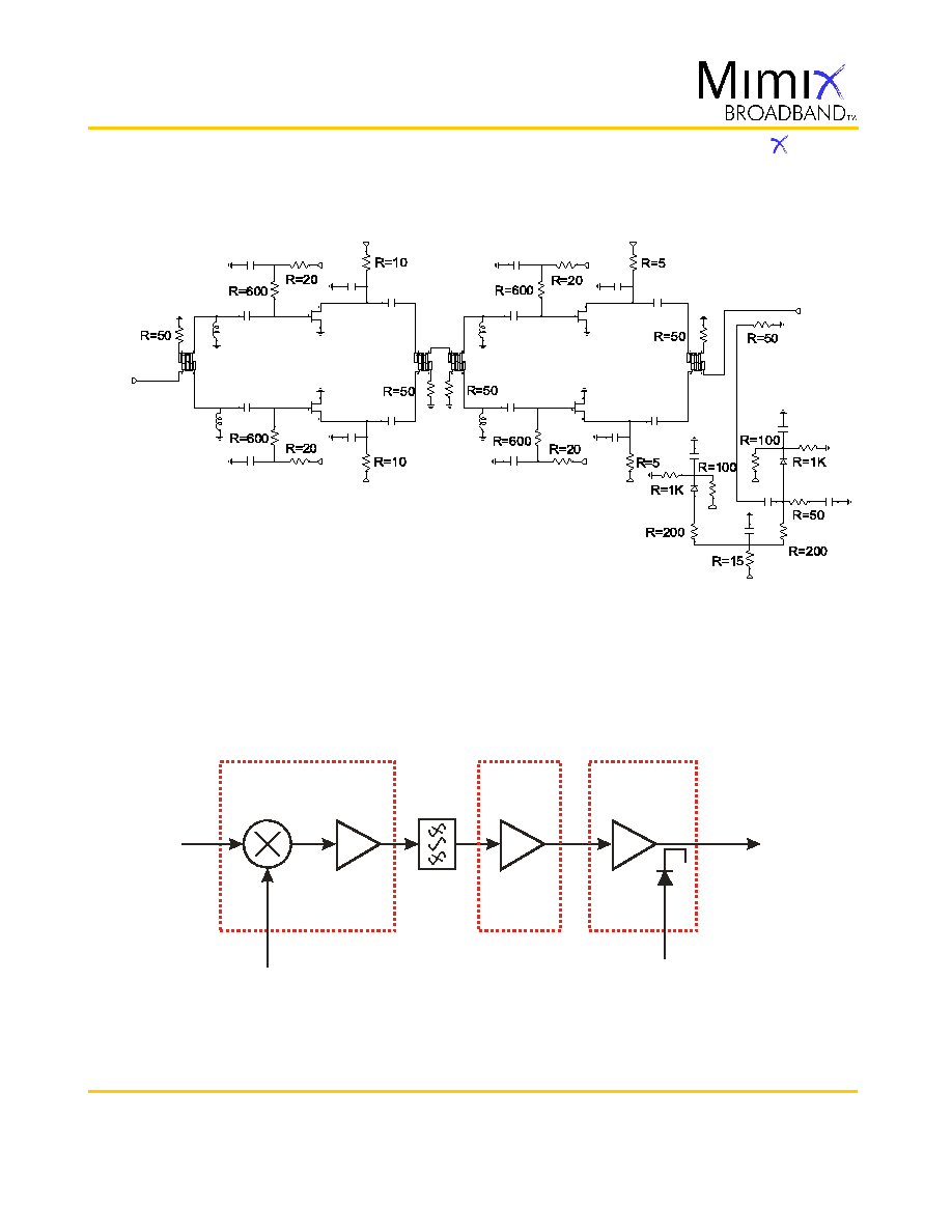
App Note [1] Biasing
-
As shown in the bonding diagram, it is recommended to separately bias the upper and lower amplifiers at
Vd(1+2)=5.5V Id(1+2)=215mA, and Vd(3+4)=5.5V Id(3+4)=215mA, although best performance will result in separately biasing Vd1
through Vd4, with Id1=Id3=71mA, Id2=Id4=144mA. It is also recommended to use active biasing to keep the currents constant as the
RF power and temperature vary; this gives the most reproducible results. Depending on the supply voltage available and the power
dissipation constraints, the bias circuit may be a single transistor or a low power operational amplifier, with a low value resistor in
series with the drain supply used to sense the current. The gate of the pHEMT is controlled to maintain correct drain current and thus
drain voltage. The typical gate voltage needed to do this is -0.5V. Typically the gate is protected with Silicon diodes to limit the
applied voltage. Also, make sure to sequence the applied voltage to ensure negative gate bias is available before applying the
positive drain supply.
App Note [2] On-board Detector
-
The output signal of the power amplifier is coupled via a 16dB directional coupler to a detector,
which comprises a diode connected to the signal path, and a second diode used to provide a temperature compensation signal. The
common bias terminal is Vd5, and is nominally set to forward bias both diodes. The bias is normally provided in 1 of 2 ways. The Vd5
port can be connected directly to a 1V bias, and given the internal series resistance, results in about 1mA of bias current. Alternatively,
Vd5 can be tied to the same voltage as Vd1-Vd4 through an external series resistor Rd in the range 3 - 6k
.
App Note [3] Bias Arrangement
-
For Parallel Stage Bias (Recommended for general applications) -- The same as Individual Stage Bias but all the drain or gate pad DC bypass
capacitors (~100-200 pF) can be combined. Additional DC bypass capacitance (~0.01 uF) is also recommended to all DC or combination (if
gate or drains are tied together) of DC bias pads.
For Individual Stage Bias -- Each DC pad (Vd1,2,3,4 and Vg1,2,3,4) needs to have DC bypass capacitance (~100-200 pF) as close to the
device as possible. Additional DC bypass capacitance (~0.01 uF) is also recommended.
MTTF Table
Backplate
Temperature
55 deg Celsius
75 deg Celsius
95 deg Celsius
Channel
Temperature
127 deg Celsius
147 deg Celsius
167 deg Celsius
FITs
1.10E+00
9.71E+00
7.04E+01
MTTF Hours
9.11E+08
1.03E+08
1.42E+07
Rth
-
30.1
∞
C/W
-
Bias Conditions: Vd1=Vd2=Vd3=5.5V, Id1=Id3=72 mA and Id2=Id4=144 mA
Mimix Broadband, Inc., 10795 Rockley Rd., Houston, Texas 77099
Tel: 281.988.4600 Fax: 281.988.4615 mimixbroadband.com
Characteristic Data and Specifications are subject to change without notice.
©2004 Mimix Broadband, Inc.
Export of this item may require appropriate export licensing from the U.S. Government. In purchasing these parts, U.S. Domestic customers accept
their obligation to be compliant with U.S. Export Laws.
These numbers were calculated based on accelerated life test information and thermal model analysis received from the fabricating foundry.
P1001
May 2005 - Rev 05-May-05
26.0-40.0 GHz GaAs MMIC
Power Amplifier
Page 5 of 6
Mimix Broadband, Inc., 10795 Rockley Rd., Houston, Texas 77099
Tel: 281.988.4600 Fax: 281.988.4615 mimixbroadband.com
Characteristic Data and Specifications are subject to change without notice.
©2004 Mimix Broadband, Inc.
Export of this item may require appropriate export licensing from the U.S. Government. In purchasing these parts, U.S. Domestic customers accept
their obligation to be compliant with U.S. Export Laws.
Typical Application
Mimix Broadband MMIC-based 36.0-40.0 GHz Transmitter Block Diagram
(Changing LO and IF frequencies as required allows design to operate as high as 40 GHz)
IF IN
2 GHz
XB1002
XP1001
XU1001
WG
Sideband
Reject
RF Out
37.0-39.5 GHz
On-Chip
Temp Comp
Detector
LO(+15dBm)
17.5-18.75 GHz (USB Operation)
19.5-20.75 GHz (LSB Operation)
Device Schematic
P1001
May 2005 - Rev 05-May-05
RF In
Vg1
Vd1
Vg3
Vd3
Vg2
Vd2
RF Out
Vout2
Vd5
Vd4
Vg4
Vout1