 | –≠–ª–µ–∫—Ç—Ä–æ–Ω–Ω—ã–π –∫–æ–º–ø–æ–Ω–µ–Ω—Ç: XP1011 | –°–∫–∞—á–∞—Ç—å:  PDF PDF  ZIP ZIP |
Velocium Products
18 - 20 GHz HPA
- APH478
36.0-40.0 GHz GaAs MMIC
Power Amplifier
Page 1 of 6
Mimix Broadband, Inc., 10795 Rockley Rd., Houston, Texas 77099
Tel: 281.988.4600 Fax: 281.988.4615 mimixbroadband.com
Characteristic Data and Specifications are subject to change without notice.
©2006 Mimix Broadband, Inc.
Export of this item may require appropriate export licensing from the U.S. Government. In purchasing these parts, U.S. Domestic customers accept
their obligation to be compliant with U.S. Export Laws.
May 2006 - Rev 10-May-06
P1011
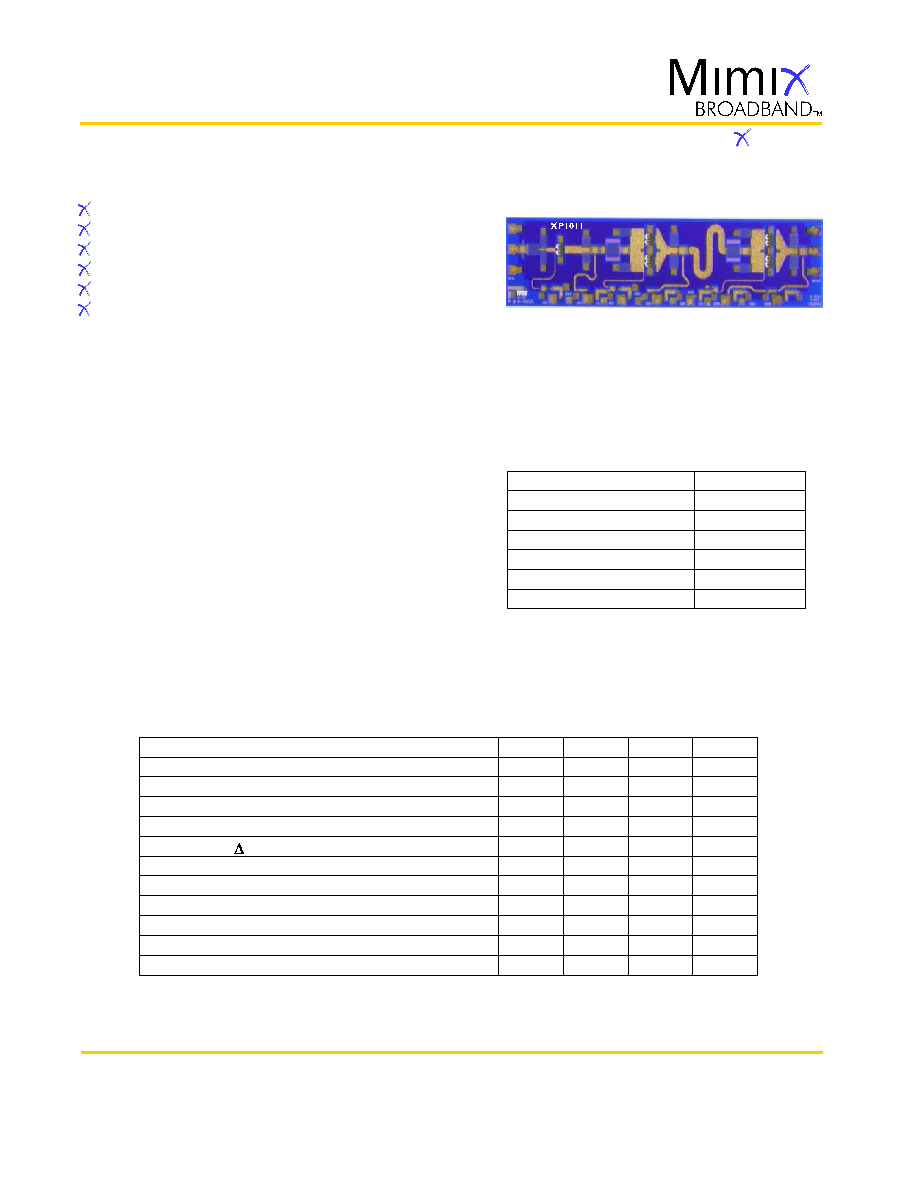
Mimix Broadband's three stage 36.0-40.0 GHz GaAs
MMIC power amplifier is optimized for linear operation
with a third order intercept point of +36.0 dBm. This
MMIC uses Mimix Broadband's 0.15 µm GaAs PHEMT
device model technology, and is based upon electron
beam lithography to ensure high repeatability and
uniformity. The chip has surface passivation to protect
and provide a rugged part with backside via holes and
gold metallization to allow either a conductive epoxy
or eutectic solder die attach process. This device is well
suited for Millimeter-wave Point-to-Point Radio, LMDS,
SATCOM and VSAT applications.
Absolute Maximum Ratings
General Description
Supply Voltage (Vd)
Supply Current (Id1,2,3)
Gate Bias Voltage
Input Power (Pin)
Storage Temperature (Tstg)
Operating Temperature (Ta)
Channel Temperature (Tch)
+5.5 VDC
155,415,715 mA
+0.3 VDC
+8 dBm
-65 to +165
O
C
-55 to MTTF TAble
MTTF Table
(3) Channel temperature affects a device's MTTF. It is
recommended to keep channel temperature as low as
possible for maximum life.
3
Features
Chip Device Layout
3
Excellent Linear Output Amplifier Stage
21.0 dB Small Signal Gain
+36.0 dBm Third Order Intercept (OIP3)
+27.0 dBm Output P1dB Compression Point
100% On-Wafer RF, DC and Output Power Testing
100% Visual Inspection to MIL-STD-883
Method 2010
Frequency Range (f )
Input Return Loss (S11)
Output Return Loss (S22)
Small Signal Gain (S21)
Gain Flatness ( S21)
Reverse Isolation (S12)
Output Power for 1 dB Compression (P1dB)
Output Third Order Intercept Point (OIP3)
Drain Bias Voltage (Vd1,2,3)
Gate Bias Voltage (Vg1,2,3)
Supply Current (Id) (Vd=5.0V, Vg=-0.5V Typical)
Electrical Characteristics (Ambient Temperature T = 25
o
C)
Parameter
Units
GHz
dB
dB
dB
dB
dB
dBm
dBm
VDC
VDC
mA
Min.
36.0
-
-
-
-
-
-
-
-
-1.0
-
Typ.
-
10.0
9.0
21.0
+/-0.5
-
+27.0
+36.0
+5.0
-0.5
640
Max.
40.0
-
-
-
-
-
-
-
-
0.0
-
(1) Measured at +18 dBm per tone output carrier level across the full frequency band.
(2) Measured using constant current.
1,2
2

Velocium Products
18 - 20 GHz HPA
- APH478
Power Amplifier Measurements
Page 2 of 6
Measured Perfor mance Characteristics (Typical Perfor mance at 25∞C)
Vd1 = Vd2 = Vd3 = 5 V, Id 1 = 100 mA, Id2 = Id3 = 270 mA
15
20
25
30
35
40
45
36
37
38
39
40
41
Fr e q u e n cy ( GHz )
Pout (dBm)
P1dB
IP3
14
16
18
20
22
24
26
28
36
37
38
39
40
41
Fr e q u e n cy ( GHz )
Ga
in (dB)
-24
-22
-20
-18
-16
-14
-12
-10
-8
-6
-4
-2
0
36
37
38
39
40
41
Fr e q u e n cy ( GHz )
Input Return Loss (dB)
-40
-36
-32
-28
-24
-20
-16
-12
-8
-4
0
36
37
38
39
40
41
Fr e q u e n cy ( GHz )
Output Return Loss (dB)
36.0-40.0 GHz GaAs MMIC
Power Amplifier
Mimix Broadband, Inc., 10795 Rockley Rd., Houston, Texas 77099
Tel: 281.988.4600 Fax: 281.988.4615 mimixbroadband.com
Characteristic Data and Specifications are subject to change without notice.
©2006 Mimix Broadband, Inc.
Export of this item may require appropriate export licensing from the U.S. Government. In purchasing these parts, U.S. Domestic customers accept
their obligation to be compliant with U.S. Export Laws.
May 2006 - Rev 10-May-06
P1011
Velocium Products
18 - 20 GHz HPA
- APH478
Page 3 of 6
S-Parameters
Measured Perfor mance Characteristics (Typical Perfor mance at 25∞C)
Vd1 = Vd2 = Vd3 = 5 V, Id 1 = 100 mA, Id2 = Id3 = 270 mA
Freq GHz S11 Mag
S11 A ng
S21 Mag
S21 Ang
S12 Mag
S12 Ang
S22 Mag
S22 A ng
36
0.257
169.682
9.752
17.572
0
88.316
0.7
154.857
36.5
0.219
157.254
10.085
-6.541
0.001
137.979
0.672
149.661
37
0.189
139.742
10.462
-30.842
0.001
149.628
0.634
144.58
37.5
0.163
113.77
10.644
-55.166
0.001
141.639
0.585
139.033
38
0.152
80.829
10.783
-79.904
0.002
138.863
0.528
134.176
38.5
0.178
53.538
10.781
-104.619
0.002
128.236
0.468
130.614
39
0.241
32.765
10.87
-129.024
0.002
119.139
0.409
128.032
39.5
0.304
16.271
10.802
-154.302
0.002
132.162
0.362
126.503
40
0.376
2.791
10.806
179.147
0.002
114.772
0.322
124.381
40.5
0.455
-8.622
10.596
151.874
0.003
127.58
0.28
121.51
41
0.539
-19.504
10.206
123.1
0.004
105.152
0.248
118.15
41.5
0.606
-29.153
9.615
93.208
0.004
86.51
0.217
110.228
42
0.662
-38.825
8.547
62.374
0.004
59.679
0.175
94.873
36.0-40.0 GHz GaAs MMIC
Power Amplifier
Mimix Broadband, Inc., 10795 Rockley Rd., Houston, Texas 77099
Tel: 281.988.4600 Fax: 281.988.4615 mimixbroadband.com
Characteristic Data and Specifications are subject to change without notice.
©2006 Mimix Broadband, Inc.
Export of this item may require appropriate export licensing from the U.S. Government. In purchasing these parts, U.S. Domestic customers accept
their obligation to be compliant with U.S. Export Laws.
May 2006 - Rev 10-May-06
P1011

Page 4 of 6
36.0-40.0 GHz GaAs MMIC
Power Amplifier
1
5
0.920
(0.036)
0.582
(0.023)
0.0
0.0
0.582
(0.023)
2.179
(0.086)
3.760
(0.148)
6
7
8
1.780
(0.070)
3
3.179
(0.125)
4
2.579
(0.102)
1.379
(0.054)
0.980
(0.039)
9
0.580
(0.023)
2
Mechanical Drawing
Units: millimeters (inches) Bond pad dimensions are shown to center of bond pad.
Thickness: 0.110 +/- 0.010 (0.0043 +/- 0.0004), Backside is ground, Bond Pad/Backside Metallization: Gold
All Bond Pads are 0.100 x 0.100 (0.004 x 0.004).
Bond pad centers are approximately 0.109 (0.004) from the edge of the chip.
Dicing tolerance: +/- 0.005 (+/- 0.0002). Approximate weight: 2.145 mg.
Bias Arrangement
Bond Pad #1 (RF In)
Bond Pad #2 (RF Out)
Bond Pad #3 (Vd3b)
Bond Pad #4 (Vd3a)
Bond Pad #5 (Vg3)
Bond Pad #6 (Vd2)
Bond Pad #7 (Vg2)
Bond Pad #8 (Vd1)
Bond Pad #9 (Vg1)
Bypass Capacitors - See App Note [2]
1
5
6
7
8
3
4
9
2
RF Out
RF In
Vd1
Vg1
10
Vg2
10
Vd2
Vg3
10
Vd3a
Vd3b
Mimix Broadband, Inc., 10795 Rockley Rd., Houston, Texas 77099
Tel: 281.988.4600 Fax: 281.988.4615 mimixbroadband.com
Characteristic Data and Specifications are subject to change without notice.
©2006 Mimix Broadband, Inc.
Export of this item may require appropriate export licensing from the U.S. Government. In purchasing these parts, U.S. Domestic customers accept
their obligation to be compliant with U.S. Export Laws.
May 2006 - Rev 10-May-06
P1011

Page 5 of 6
App Note [1] Biasing
-
It is recommended to separately bias each stage at Vd(1,2,3)=5.0V, Id1=100mA, Id2=270mA, and Id3=270mA. It
is also recommended to use active biasing to keep the currents constant as the RF power and temperature vary; this gives the most
reproducible results. Depending on the supply voltage available and the power dissipation constraints, the bias circuit may be a
single transistor or a low power operational amplifier, with a low value resistor in series with the drain supply used to sense the
current. The gate of the pHEMT is controlled to maintain correct drain current and thus drain voltage. The typical gate voltage needed
to do this is -0.5V. Typically the gate is protected with Silicon diodes to limit the applied voltage. Also, make sure to sequence the
applied voltage to ensure negative gate bias is available before applying the positive drain supply.
App Note [2] Bias Arrangement
-
For Parallel Stage Bias (Recommended for general applications) -- The same as Individual Stage Bias but all the drain or gate pad DC
bypass capacitors (~100-200 pF) can be combined. Additional DC bypass capacitance (~0.01 uF) is also recommended to all DC or
combination (if gate or drains are tied together) of DC bias pads.
For Individual Stage Bias (Recommended for Saturated Applications) -- Each DC pad (Vd1,2,3 and Vg1,2,3) needs to have DC bypass
capacitance (~100-200 pF) as close to the device as possible. Additional DC bypass capacitance (~0.01 uF) is also recommended.
MTTF Table (TBD)
Backplate
Temperature
55 deg Celsius
75 deg Celsius
95 deg Celsius
Channel
Temperature
deg Celsius
deg Celsius
deg Celsius
FITs
E+
E+
E+
MTTF Hours
E+
E+
E+
Rth
C/W
C/W
C/W
Bias Conditions: Vd1=Vd2=Vd3=5.0V, Id1=100 mA, Id2=270 mA, Id3=270 mA
These numbers were calculated based on accelerated life test information and thermal model analysis received from the fabricating foundry.
36.0-40.0 GHz GaAs MMIC
Power Amplifier
Mimix Broadband, Inc., 10795 Rockley Rd., Houston, Texas 77099
Tel: 281.988.4600 Fax: 281.988.4615 mimixbroadband.com
Characteristic Data and Specifications are subject to change without notice.
©2006 Mimix Broadband, Inc.
Export of this item may require appropriate export licensing from the U.S. Government. In purchasing these parts, U.S. Domestic customers accept
their obligation to be compliant with U.S. Export Laws.
May 2006 - Rev 10-May-06
P1011