 | –≠–ª–µ–∫—Ç—Ä–æ–Ω–Ω—ã–π –∫–æ–º–ø–æ–Ω–µ–Ω—Ç: XP1013 | –°–∫–∞—á–∞—Ç—å:  PDF PDF  ZIP ZIP |

Mimix Broadband, Inc., 10795 Rockley Rd., Houston, Texas 77099
Tel: 281.988.4600 Fax: 281.988.4615 mimixbroadband.com
Characteristic Data and Specifications are subject to change without notice.
©2005 Mimix Broadband, Inc.
Export of this item may require appropriate export licensing from the U.S. Government. In purchasing these parts, U.S. Domestic customers accept
their obligation to be compliant with U.S. Export Laws.
May 2005 - Rev 05-May-05
Mimix Broadband
's three stage 17.0-26.0 GHz GaAs
MMIC power amplifier has a small signal gain of 20.0
dB with a +24.0 dBm saturated output power. This
MMIC uses Mimix Broadband
's 0.15 µm GaAs PHEMT
device model technology, and is based upon electron
beam lithography to ensure high repeatability and
uniformity. The chip has surface passivation to protect
and provide a rugged part with backside via holes
and gold metallization to allow either a conductive
epoxy or eutectic solder die attach process. This
device is well suited for Millimeter-wave Point-to-
Point Radio, LMDS, SATCOM and VSAT applications.
17.0-26.0 GHz GaAs MMIC
Power Amplifier
Excellent Saturated Output Stage
Competitive RF/DC Bias Pin for Pin Replacement
20.0 dB Small Signal Gain
+24.0 dBm Saturated Output Power
100% On-Wafer RF, DC and Output Power Testing
100% Visual Inspection to MIL-STD-883
Method 2010
Features
General Description
Electrical Characteristics (Ambient Temperature T = 25
o
C)
Parameter
Frequency Range (f )
Input Return Loss (S11)
Output Return Loss (S22)
Small Signal Gain (S21)
Gain Flatness (
S21)
Reverse Isolation (S12)
Saturated Output Power (Psat)
Drain Bias Voltage (Vd1,2,3)
Gate Bias Voltage (Vg1,2,3)
Supply Current (Id) (Vd=6.0V, Vg=-0.7V Typical)
Units
GHz
dB
dB
dB
dB
dB
dBm
VDC
VDC
mA
Min.
17.0
-
-
-
-
-
-
-
-1.0
-
Typ.
-
10.0
10.0
20.0
+/-2.0
50.0
+24.0
+6.0
-0.7
320
Max.
26.0
-
-
-
-
-
-
+8.0
0.0
480
Absolute Maximum Ratings
Supply Voltage (Vd)
Supply Current (Id)
Gate Bias Voltage (Vg)
Input Power (Pin)
Storage Temperature (Tstg)
Operating Temperature (Ta)
Channel Temperature (Tch)
+9.0 VDC
650 mA
+0.3 VDC
+5.0 dBm
-65 to +165
O
C
-55 to MTTF Table
MTTF Table
Chip Device Layout
Page 1 of 7
1
(1) Channel temperature affects a device's MTTF. It is
recommended to keep channel temperature as low as
possible for maximum life.
1
P1013

Mimix Broadband, Inc., 10795 Rockley Rd., Houston, Texas 77099
Tel: 281.988.4600 Fax: 281.988.4615 mimixbroadband.com
Characteristic Data and Specifications are subject to change without notice.
©2005 Mimix Broadband, Inc.
Export of this item may require appropriate export licensing from the U.S. Government. In purchasing these parts, U.S. Domestic customers accept
their obligation to be compliant with U.S. Export Laws.
0.045
10
20
30
40
50
Frequency (GHz)
S12
-120
-100
-80
-60
-40
DB(|S[1,2]|)
All Sources
17.0-26.0 GHz GaAs MMIC
Power Amplifier
Power Amplifier Measurements
Page 2 of 7
0.045
10
20
30
40
50
Frequency (GHz)
S21
-40
-20
0
20
30
DB(|S[2,1]|)
All Sources
0.045
10
20
30
40
50
Frequency (GHz)
S11
-25
-20
-15
-10
-5
0
DB(|S[1,1]|)
All Sources
0.045
10
20
30
40
50
Frequency (GHz)
S22
-25
-20
-15
-10
-5
0
DB(|S[2,2]|)
All Sources
May 2005 - Rev 05-May-05
P1013
Mimix Broadband, Inc., 10795 Rockley Rd., Houston, Texas 77099
Tel: 281.988.4600 Fax: 281.988.4615 mimixbroadband.com
Characteristic Data and Specifications are subject to change without notice.
©2005 Mimix Broadband, Inc.
Export of this item may require appropriate export licensing from the U.S. Government. In purchasing these parts, U.S. Domestic customers accept
their obligation to be compliant with U.S. Export Laws.
17.0-26.0 GHz GaAs MMIC
Power Amplifier
Power Amplifier Measurements (cont.)
Page 3 of 7
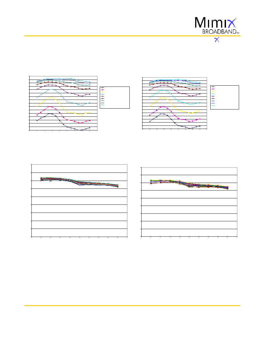
0289: Pout vs. freq, Pin = 0dBm
10
12
14
16
18
20
22
24
26
28
17
18
19
20
21
22
23
24
25
26
27
freq (GHz)
Pou
t (dB
m
)
0289: Pout vs. freq
Pin = 0dBm
10
12
14
16
18
20
22
24
26
28
17
18
19
20
21
22
23
24
25
26
27
freq (GHz)
Po
u
t
(d
B
m
)
0289_R4C2 (Vd1 = 6.0V, Id1 = 50mA, Vd2 = 6.0V, Id2 = 90mA, Vd3 = 6.0V, Id3 =
180mA): Pout vs. freq
10
11
12
13
14
15
16
17
18
19
20
21
22
23
24
25
26
16
17
18
19
20
21
22
23
24
25
freq (GHz)
P
out
(
d
Bm
)
, MeasFile=4_0289_R4C2_22082003_1726_-12dBm.pin
, MeasFile=4_0289_R4C2_22082003_1728_-10dBm.pin
, MeasFile=4_0289_R4C2_22082003_1730_-8dBm.pin
, MeasFile=4_0289_R4C2_22082003_1732_-6dBm.pin
, MeasFile=4_0289_R4C2_22082003_1733_-4dBm.pin
, MeasFile=4_0289_R4C2_22082003_1735_-2dBm.pin
, MeasFile=4_0289_R4C2_22082003_1736_0dBm.pin
, MeasFile=4_0289_R4C2_22082003_1738_2dBm.pin
, MeasFile=4_0289_R4C2_22082003_1739_4dBm.pin
, MeasFile=4_0289_R4C2_22082003_1740_6dBm.pin
0289_R3C4 (Vd1 = 6.0V, Id1 = 50mA, Vd2 = 6.0V, Id2 = 90mA, Vd3 = 6.0V, Id3 =
180mA): Pout vs. freq
10
11
12
13
14
15
16
17
18
19
20
21
22
23
24
25
26
16
17
18
19
20
21
22
23
24
25
freq (GHz)
Po
u
t
(d
B
m
)
, MeasFile=4_0289_R3C4_25082003_0952_-12dBm.pin
, MeasFile=4_0289_R3C4_25082003_0954_-10dBm.pin
, MeasFile=4_0289_R3C4_25082003_0957_-8dBm.pin
, MeasFile=4_0289_R3C4_25082003_1000_-6dBm.pin
, MeasFile=4_0289_R3C4_25082003_1001_-4dBm.pin
, MeasFile=4_0289_R3C4_25082003_1003_-2dBm.pin
, MeasFile=4_0289_R3C4_25082003_1005_0dBm.pin
, MeasFile=4_0289_R3C4_25082003_1030_2dBm.pin
, MeasFile=4_0289_R3C4_25082003_1032_4dBm.pin
, MeasFile=4_0289_R3C4_25082003_1034_6dBm.pin
May 2005 - Rev 05-May-05
P1013

1
2
3
4
5
6
7
8
Vd1,2,3
RF In
RF Out
Vg1,2,3
1.145
(0.045)
1
2
3
4
5
6
7
8
1.207
(0.048)
1.539
(0.061)
2.405
(0.095)
1.478
(0.058)
2.550
(0.100)
0.808
(0.032)
0.431
(0.017)
0.0
0.0
0.549
(0.022)
0.490
(0.019)
Mimix Broadband, Inc., 10795 Rockley Rd., Houston, Texas 77099
Tel: 281.988.4600 Fax: 281.988.4615 mimixbroadband.com
Characteristic Data and Specifications are subject to change without notice.
©2005 Mimix Broadband, Inc.
Export of this item may require appropriate export licensing from the U.S. Government. In purchasing these parts, U.S. Domestic customers accept
their obligation to be compliant with U.S. Export Laws.
17.0-26.0 GHz GaAs MMIC
Power Amplifier
Page 4 of 7
Mechanical Drawing
Bias Arrangement
Bypass Capacitors - See App Note [2]
(Note: Engineering designator is 20MPA0289)
Units: millimeters (inches) Bond pad dimensions are shown to center of bond pad.
Thickness: 0.110 +/- 0.010 (0.0043 +/- 0.0004), Backside is ground, Bond Pad/Backside Metallization: Gold
All DC Bond Pads are 0.100 x 0.100 (0.004 x 0.004). All RF Bond Pads are 0.100 x 0.200 (0.004 x 0.008)
Bond pad centers are approximately 0.109 (0.004) from the edge of the chip.
Dicing tolerance: +/- 0.005 (+/- 0.0002). Approximate weight: 1.807 mg.
Bond Pad #1 (RF In)
Bond Pad #2 (Vd1)
Bond Pad #3 (Vd2)
Bond Pad #4 (Vd3)
Bond Pad #5 (RF Out)
Bond Pad #6 (Vg3)
Bond Pad #7 (Vg2)
Bond Pad #8 (Vg1)
May 2005 - Rev 05-May-05
P1013
Vd1,2,3
RF In
Vg1,2,3
RF Out

Mimix Broadband, Inc., 10795 Rockley Rd., Houston, Texas 77099
Tel: 281.988.4600 Fax: 281.988.4615 mimixbroadband.com
Characteristic Data and Specifications are subject to change without notice.
©2005 Mimix Broadband, Inc.
Export of this item may require appropriate export licensing from the U.S. Government. In purchasing these parts, U.S. Domestic customers accept
their obligation to be compliant with U.S. Export Laws.
17.0-26.0 GHz GaAs MMIC
Power Amplifier
Page 5 of 7
App Note [1] Biasing
-
It is recommended to separately bias each amplifier stage Vd1 through Vd3 at Vd(1,2,3)=6.0V with Id1=47mA,
Id2=90mA and Id3=180mA. Separate biasing is recommended if the amplifier is to be used at high levels of saturation, where gate
rectification will alter the effective gate control voltage. For non-critical applications it is possible to parallel all stages and adjust the
common gate voltage for a total drain current Id(total)=320 mA. It is also recommended to use active biasing to keep the currents
constant as the RF power and temperature vary; this gives the most reproducible results. Depending on the supply voltage available
and the power dissipation constraints, the bias circuit may be a single transistor or a low power operational amplifier, with a low
value resistor in series with the drain supply used to sense the current. The gate of the pHEMT is controlled to maintain correct drain
current and thus drain voltage. The typical gate voltage needed to do this is -0.7V. Typically the gate is protected with Silicon diodes
to limit the applied voltage. Also, make sure to sequence the applied voltage to ensure negative gate bias is available before
applying the positive drain supply.
App Note [2] Bias Arrangement
-
For Parallel Stage Bias (Recommended for general applications) -- The same as Individual Stage Bias but all the drain or gate pad DC
bypass capacitors (~1000-2200 pF) can be combined. Additional DC bypass capacitance (~0.01 uF) is also recommended to all DC or
combination (if gate or drains are tied together) of DC bias pads.
For Individual Stage Bias (Recommended for saturated applications) -- Each DC pad (Vd1, 2, 3 and Vg1, 2, 3) needs to have DC bypass
capacitance (~1000-2200 pF) as close to the device as possible. Additional DC bypass capacitance (~0.01 uF) is also recommended.
MTTF Tables
Backplate
Temperature
55 deg Celsius
75 deg Celsius
95 deg Celsius
Channel
Temperature
176.3 deg Celsius
204.0 deg Celsius
231.1 deg Celsius
FITs
1.02E+02
1.07E+03
8.30E+03
MTTF Hours
9.79E+06
9.32E+05
1.21E+05
Rth
63.8
∞
C/W
67.8
∞
C/W
71.6
∞
C/W
Bias Conditions:
Vd1=Vd2=Vd3=6.0V, Id1=47 mA, Id2=90 mA, Id3=180 mA
These numbers were calculated based on accelerated life test information and thermal model analysis received from the fabricating foundry.
May 2005 - Rev 05-May-05
P1013