 | –≠–ª–µ–∫—Ç—Ä–æ–Ω–Ω—ã–π –∫–æ–º–ø–æ–Ω–µ–Ω—Ç: XU1004 | –°–∫–∞—á–∞—Ç—å:  PDF PDF  ZIP ZIP |
Mimix Broadband, Inc., 10795 Rockley Rd., Houston, Texas 77099
Tel: 281.988.4600 Fax: 281.988.4615 mimixbroadband.com
Characteristic Data and Specifications are subject to change without notice.
©2005 Mimix Broadband, Inc.
Export of this item may require appropriate export licensing from the U.S. Government. In purchasing these parts, U.S. Domestic customers accept
their obligation to be compliant with U.S. Export Laws.
May 2005 - Rev 20-May-05
Mimix Broadband
's 32.0-45.0 GHz GaAs MMIC transmitter has a
+14.0 dBm output third order intercept across the band. This
device is a balanced, resistive pHEMT mixer followed by a
distributed output amplifier and includes an integrated LO
doubler and LO buffer amplifier. The use of integrated LO
doubler and LO buffer amplifier makes the provision of the LO
easier than for fundamental mixers at these frequencies. IF and
IF mixer inputs are provided and an external 180 degree hybrid
is required to select the desired sideband. This MMIC uses
Mimix Broadband
's 0.15 µm GaAs PHEMT device model
technology, and is based upon electron beam lithography to
ensure high repeatability and uniformity. The chip has surface
passivation to protect and provide a rugged part with backside
via holes and gold metallization to allow either a conductive
epoxy or eutectic solder die attach process. This device is well
suited for Millimeter-wave Point-to-Point Radio, LMDS, SATCOM
and VSAT applications.
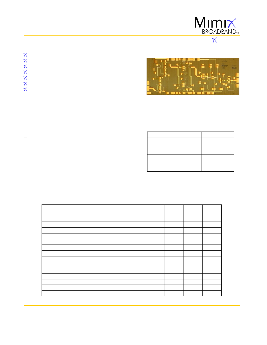
32.0-45.0 GHz GaAs MMIC
Transmitter
Electrical Characteristics (Ambient Temperature T = 25
o
C)
Page 1 of 7
Sub-harmonic Transmitter
Integrated Mixer, LO Doubler/Buffer & Output Amplifier
+14.0 dBm Output Third Order Intercept (OIP3)
+4.0 dBm LO Drive Level
5.0 dB Conversion Gain
100% On-Wafer RF and DC Testing
100% Visual Inspection to MIL-STD-883 Method 2010
Features
General Description
Absolute Maximum Ratings
Supply Voltage (Vd)
Supply Current (Id1,Id2)
Gate Bias Voltage (Vg)
Input Power (IF Pin)
Storage Temperature (Tstg)
Operating Temperature (Ta)
Channel Temperature (Tch)
+6.0 VDC
200, 180 mA
+0.3 VDC
0.0 dBm
-65 to +165
O
C
-55 to MTTF Table
MTTF Table
Chip Device Layout
Units
GHz
GHz
GHz
GHz
dB
dB
dBm
dB
dB
dBm
VDC
VDC
VDC
mA
mA
Min.
35.0
32.0
16.0
DC
-
-
-
-
-
-
-
-1.2
-1.2
-
-
Typ.
-
-
-
-
10.0
5.0
+4.0
TBD
TBD
+14.0
+4.0
-0.3
-0.5
160
145
Max.
45.0
42.0
25.0
4.0
-
-
-
-
-
-
+5.5
+0.1
+0.1
180
165
Parameter
Frequency Range (RF) Upper Side Band
Frequency Range (RF) Lower Side Band
Frequency Range (LO)
Frequency Range (IF)
Output Return Loss RF (S22)
Small Signal Conversion Gain IF/RF (S21)
LO Input Drive (P
LO
)
Isolation LO/RF @ LOx1
Isolation LO/RF @ LOx2
Output Third Order Intercept (OIP3)
Drain Bias Voltage (Vd1,2)
Gate Bias Voltage (Vg1,2)
Gate Bias Voltage (Vg3,4) Mixer, Doubler
Supply Current (Id1) (Vd1=4.0V, Vg=-0.3V Typical)
Supply Current (Id2) (Vd2=4.0V, Vg=-0.3V Typical)
(1) Measured using constant current.
(2) Measured using LO Input drive level of 0.0 dBm.
(3) Channel temperature affects a device's MTTF. It is
recommended to keep channel temperature as low as
possible for maximum life.
3
1,2
3
2
U1004

Mimix Broadband, Inc., 10795 Rockley Rd., Houston, Texas 77099
Tel: 281.988.4600 Fax: 281.988.4615 mimixbroadband.com
Characteristic Data and Specifications are subject to change without notice.
©2005 Mimix Broadband, Inc.
Export of this item may require appropriate export licensing from the U.S. Government. In purchasing these parts, U.S. Domestic customers accept
their obligation to be compliant with U.S. Export Laws.
Page 2 of 7
Transmitter Measurements
May 2005 - Rev 20-May-05
32.0-45.0 GHz GaAs MMIC
Transmitter
U1004
XU1004 Vd1,2=4.0 V, Id1=160 mA, Id2=145 mA, USB
LO=+0.0 dBm, IF=2.0 GHz @ -15.0 dBm, ~1310 Devices
-5
-4
-3
-2
-1
0
1
2
3
4
5
6
7
8
9
10
30.0
31.0
32.0
33.0
34.0
35.0
36.0
37.0
38.0
39.0
40.0
41.0
42.0
43.0
44.0
45.0
RF Fre que ncy (GHz )
C
onv
e
r
s
i
on G
a
i
n
(
d
B
)
Max
Median
Mean
-3sigma
XU1004 Vd1,2=4.0 V, Id1=160 mA, Id2=145 mA, LSB
LO=+0.0 dBm, IF=2.0 GHz @ -15.0 dBm, ~1310 Devices
-5
-4
-3
-2
-1
0
1
2
3
4
5
6
7
8
9
10
30.0
31.0
32.0
33.0
34.0
35.0
36.0
37.0
38.0
39.0
40.0
41.0
42.0
43.0
44.0
45.0
RF Fre que ncy (GHz )
C
o
n
v
e
r
s
i
o
n
G
a
in
(
d
B
)
Max
Median
Mean
-3sigma
XU1004 Vd1,2=4.0 V, Id1=160 mA, Id2=145 mA, USB/LSB
LO=+0.0 dBm, IF=2.0 GHz @ -15.0 dBm, ~1680 Devices
-30
-25
-20
-15
-10
-5
0
30.0
31.0
32.0
33.0
34.0
35.0
36.0
37.0
38.0
39.0
40.0
41.0
42.0
43.0
44.0
45.0
RF Fre que ncy (GHz )
R
F
Retu
r
n
L
o
ss
(d
B
)
Max
Median
Mean
-3sigma

Mimix Broadband, Inc., 10795 Rockley Rd., Houston, Texas 77099
Tel: 281.988.4600 Fax: 281.988.4615 mimixbroadband.com
Characteristic Data and Specifications are subject to change without notice.
©2005 Mimix Broadband, Inc.
Export of this item may require appropriate export licensing from the U.S. Government. In purchasing these parts, U.S. Domestic customers accept
their obligation to be compliant with U.S. Export Laws.
Page 3 of 7
Mechanical Drawing
Bias Arrangement
Bypass Capacitors
- See App Note [2]
(Note: Engineering designator is 40TX0531)
Units: millimeters (inches) Bond pad dimensions are shown to center of bond pad.
Thickness: 0.110 +/- 0.013 (0.0043 +/- 0.0004), Backside is ground, Bond Pad/Backside Metallization: Gold
All DC/IF Bond Pads are 0.100 x 0.100 (0.004 x 0.004). All RF Bond Pads are 0.100 x 0.200 (0.004 x 0.008)
Bond pad centers are approximately 0.109 (0.004) from the edge of the chip.
Dicing tolerance: +/- 0.005 (+/- 0.0002). Approximate weight: 3.987 mg.
Bond Pad #1 (RF Out)
Bond Pad #2 (Vd1)
Bond Pad #3 (IF1)
Bond Pad #4 (Vd2)
Bond Pad #5 (LO)
Bond Pad #6 (Vg4)
Bond Pad #7 (Vg2)
Bond Pad #8 (Vg3)
Bond Pad #7 (IF2)
Bond Pad #8 (Vg1)
May 2005 - Rev 20-May-05
32.0-45.0 GHz GaAs MMIC
Transmitter
U1004
1
2
3
4
5
6
7
8
0.295
(0.080)
1.620
(0.041)
0.921
(0.234)
1.621
(0.041)
2.220
(0.056)
3.970
(0.101)
0.646
(0.016)
2.821
(0.072)
2.421
(0.062)
2.021
(0.051)
9
10
1.621
(0.041)
0.921
(0.023)
0.0
0.0
1
2
3
4
5
6
7
8
9
10
Vg1
Vg3
Vg4
Vg2
IF2
LO
Vd2
IF1
Vd1
RF
Vd1
Vd2
IF1
Vg4
LO
IF2
Vg2
Vg3
Vg1
RF
Mimix Broadband, Inc., 10795 Rockley Rd., Houston, Texas 77099
Tel: 281.988.4600 Fax: 281.988.4615 mimixbroadband.com
Characteristic Data and Specifications are subject to change without notice.
©2005 Mimix Broadband, Inc.
Export of this item may require appropriate export licensing from the U.S. Government. In purchasing these parts, U.S. Domestic customers accept
their obligation to be compliant with U.S. Export Laws.
Page 4 of 7
MTTF Tables (TBD)
Backplate
Temperature
55 deg Celsius
75 deg Celsius
95 deg Celsius
Channel
Temperature
deg Celsius
deg Celsius
deg Celsius
FITs
E+
E+
E+
MTTF Hours
E+
E+
E+
Rth
C/W
C/W
C/W
Bias Conditions:
Vd1=Vd2=4.0V, Id1=160 mA, Id2=145 mA
These numbers were calculated based on accelerated life test information and thermal model analysis received from the fabricating foundry.
App Note [1] Biasing
- As shown in the bonding diagram, this device is operated by separately biasing Vd1 and Vd2 with Vd(1,2)=4.0V,
Id1=160mA and Id2=145mA. Additionally, a mixer and doubler bias are also required with Vg3=Vg4=-0.5V. Adjusting Vg3 and Vg4 above or
below this value can adversely affect conversion gain, LO/RF isolation and intercept point performance. It is also recommended to use active
biasing to keep the currents constant as the RF power and temperature vary; this gives the most reproducible results. Depending on the
supply voltage available and the power dissipation constraints, the bias circuit may be a single transistor or a low power operational
amplifier, with a low value resistor in series with the drain supply used to sense the current. The gate of the pHEMT is controlled to maintain
correct drain current and thus drain voltage. The typical gate voltage needed to do this is -0.3V. Typically the gate is protected with Silicon
diodes to limit the applied voltage. Also, make sure to sequence the applied voltage to ensure negative gate bias is available before applying
the positive drain supply.
App Note [2] Bias Arrangement
-
For Parallel Stage Bias (Recommended for general applications) -- The same as Individual Stage Bias but all the drain or gate pad DC bypass
capacitors (~100-200 pF) can be combined. Additional DC bypass capacitance (~0.01 uF) is also recommended to all DC or combination (if
gate or drains are tied together) of DC bias pads.
For Individual Stage Bias -- Each DC pad (Vd1,2 and Vg1,2,3,4) needs to have DC bypass capacitance (~100-200 pF) as close to the device as
possible. Additional DC bypass capacitance (~0.01 uF) is also recommended.
May 2005 - Rev 20-May-05
32.0-45.0 GHz GaAs MMIC
Transmitter
U1004
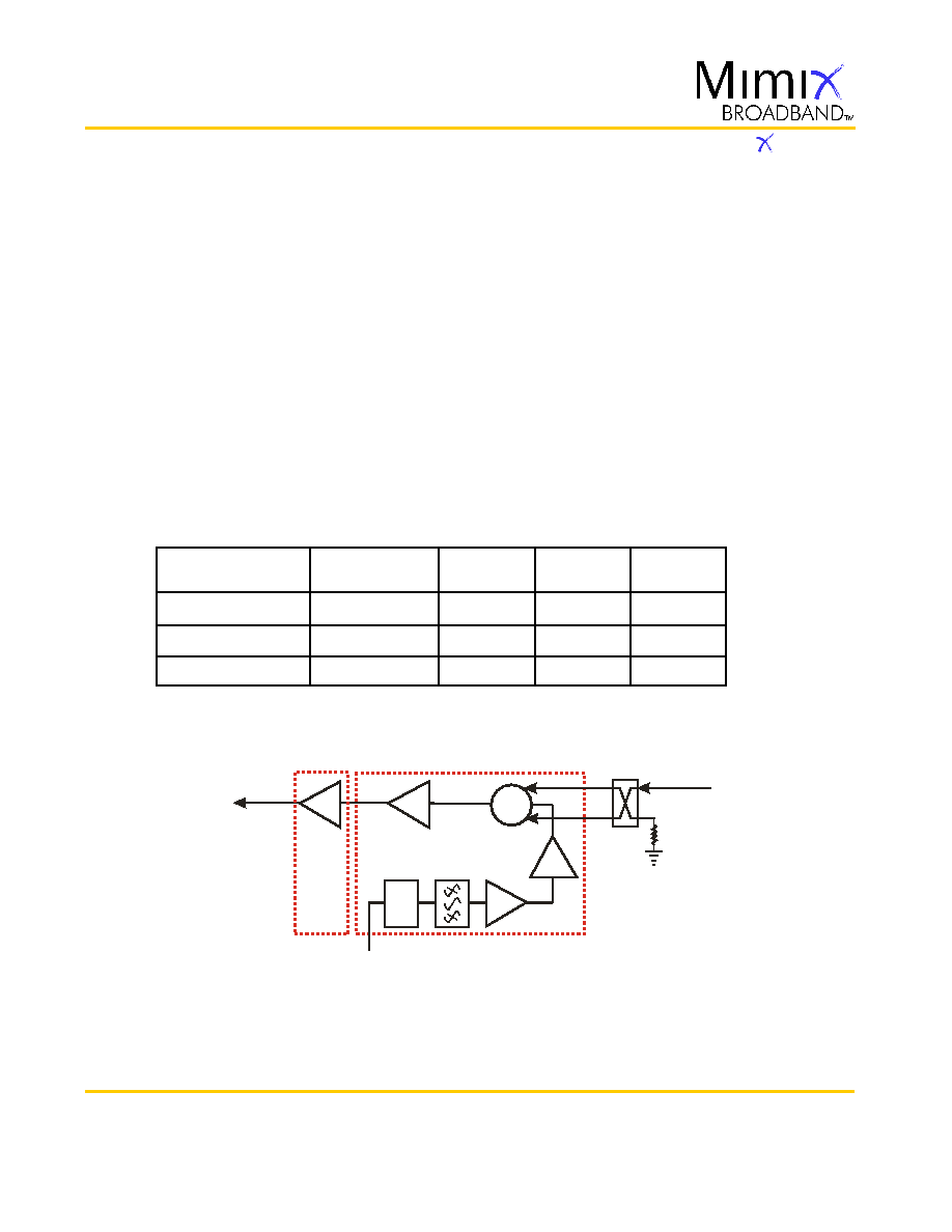
Typical Application
Mimix Broadband's 32.0-45.0 GHz XU1004 GaAs MMIC Transmitter can be used in saturated radio applications and linear modulation
schemes up to 128 QAM. The receiver can be used in upper and lower sideband applications from 32.0-45.0 GHz.
Mixer
Mimix
Broadband MMIC-based 32.0-45.0 GHz Receiver Block Diagram
(Changing LO and IF frequencies as required allows design to operate as high as 45 GHz)
RF OUT
37.0-39.5 GHz
XU1004
XP1005
Coupler
IF In
2 GHz
LO(+2.0dBm)
17.5-18.75 GHz (USB Operation)
19.5-20.75 GHz (LSB Operation)
Buffer
X2
X

Mimix Broadband, Inc., 10795 Rockley Rd., Houston, Texas 77099
Tel: 281.988.4600 Fax: 281.988.4615 mimixbroadband.com
Characteristic Data and Specifications are subject to change without notice.
©2005 Mimix Broadband, Inc.
Export of this item may require appropriate export licensing from the U.S. Government. In purchasing these parts, U.S. Domestic customers accept
their obligation to be compliant with U.S. Export Laws.
Page 5 of 7
May 2005 - Rev 20-May-05
32.0-45.0 GHz GaAs MMIC
Transmitter
U1004
App Note [3] USB/LSB Selection
-
USB
LSB
IF1
IF2
An alternate method of Selection of USB or LSB:
For Lower Side Band operation (LSB):
With IF1 and IF2 connected to the
direct port (0∫) and coupled port (180∫)
respectively as shown in the diagram,
the LSB signal will reside on the input
port. The isolated port must be loaded
with 50 ohms.
With IF1 and IF2 connected to the
direct port (0∫) and coupled port (180∫)
respectively as shown in the diagram,
the USB signal will reside on the
isolated port. The input port must be
loaded with 50 ohms.
For Upper Side Band operation (USB):
-180∫
In Phase Combiner
USB
In Phase Combiner
LSB
-180∫
IF2
IF1
IF2
IF1
Mimix Broadband, Inc., 10795 Rockley Rd., Houston, Texas 77099
Tel: 281.988.4600 Fax: 281.988.4615 mimixbroadband.com
Characteristic Data and Specifications are subject to change without notice.
©2005 Mimix Broadband, Inc.
Export of this item may require appropriate export licensing from the U.S. Government. In purchasing these parts, U.S. Domestic customers accept
their obligation to be compliant with U.S. Export Laws.
Page 6 of 7
May 2005 - Rev 20-May-05
32.0-45.0 GHz GaAs MMIC
Transmitter
U1004
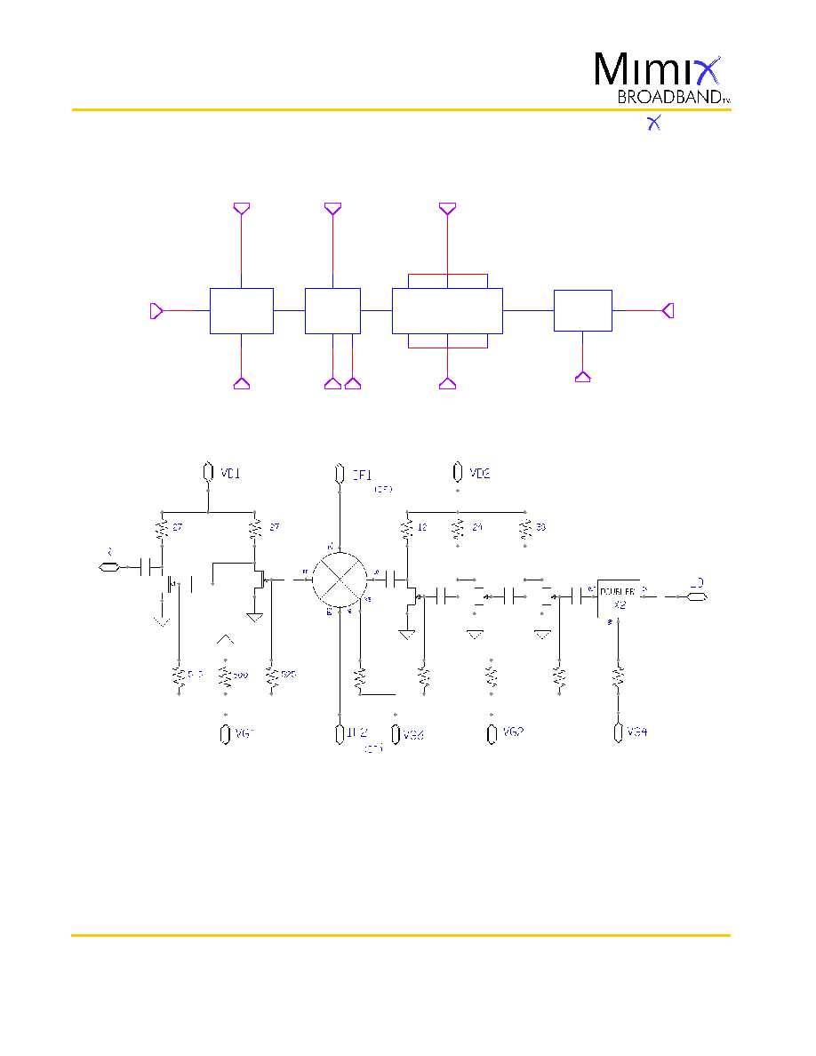
Device Schematic
Block Diagram
RF Out
Vg1
IF1
Vd2
Vg2
IF2
Vg3
LO In
LO Out
LO
RF
RF Out
RF In
Vd1
LO Buffer
Mixer
Output Amp
LO
Vg5
LO In
LO Out
Doubler

Mimix Broadband, Inc., 10795 Rockley Rd., Houston, Texas 77099
Tel: 281.988.4600 Fax: 281.988.4615 mimixbroadband.com
Characteristic Data and Specifications are subject to change without notice.
©2005 Mimix Broadband, Inc.
Export of this item may require appropriate export licensing from the U.S. Government. In purchasing these parts, U.S. Domestic customers accept
their obligation to be compliant with U.S. Export Laws.
Page 7 of 7
Handling and Assembly Information
CAUTION! - Mimix Broadband MMIC Products contain gallium arsenide (GaAs) which can be hazardous to the
human body and the environment. For safety, observe the following procedures:
Do not ingest.
Do not alter the form of this product into a gas, powder, or liquid through burning, crushing, or chemical
processing as these by-products are dangerous to the human body if inhaled, ingested, or swallowed.
Observe government laws and company regulations when discarding this product. This product must be
discarded in accordance with methods specified by applicable hazardous waste procedures.
Life Support Policy - Mimix Broadband's products are not authorized for use as critical components in life support
devices or systems without the express written approval of the President and General Counsel of Mimix
Broadband. As used herein: (1) Life support devices or systems are devices or systems which, (a) are intended for
surgical implant into the body, or (b) support or sustain life, and whose failure to perform when properly used in
accordance with instructions for use provided in the labeling, can be reasonably expected to result in a
significant injury to the user. (2) A critical component is any component of a life support device or system whose
failure to perform can be reasonably expected to cause the failure of the life support device or system, or to
affect its safety or effectiveness.
ESD - Gallium Arsenide (GaAs) devices are susceptible to electrostatic and mechanical damage. Die are supplied
in antistatic containers, which should be opened in cleanroom conditions at an appropriately grounded anti-
static workstation. Devices need careful handling using correctly designed collets, vacuum pickups or, with care,
sharp tweezers.
Die Attachment - GaAs Products from Mimix Broadband are 0.100 mm (0.004") thick and have vias through to the
backside to enable grounding to the circuit. Microstrip substrates should be brought as close to the die as
possible. The mounting surface should be clean and flat. If using conductive epoxy, recommended epoxies are
Ablestick 84-1LMI or 84-1LMIT cured in a nitrogen atmosphere per manufacturer's cure schedule. Apply epoxy
sparingly to avoid getting any on to the top surface of the die. An epoxy fillet should be visible around the total
die periphery. If eutectic mounting is preferred, then a fluxless gold-tin (AuSn) preform, approximately 0.001
thick, placed between the die and the attachment surface should be used. A die bonder that utilizes a heated
collet and provides scrubbing action to ensure total wetting to prevent void formation in a nitrogen atmosphere
is recommended. The gold-tin eutectic (80% Au 20% Sn) has a melting point of approximately 280 C (Note: Gold
Germanium should be avoided). The work station temperature should be 310 C 10 C. Exposure to these
extreme temperatures should be kept to minimum. The collet should be heated, and the die pre-heated to avoid
excessive thermal shock. Avoidance of air bridges and force impact are critical during placement.
Wire Bonding - Windows in the surface passivation above the bond pads are provided to allow wire bonding to
the die's gold bond pads. The recommended wire bonding procedure uses 0.076 mm x 0.013 mm (0.003" x
0.0005") 99.99% pure gold ribbon with 0.5-2% elongation to minimize RF port bond inductance. Gold 0.025 mm
(0.001") diameter wedge or ball bonds are acceptable for DC Bias connections. Aluminum wire should be
avoided. Thermo-compression bonding is recommended though thermosonic bonding may be used providing
the ultrasonic content of the bond is minimized. Bond force, time and ultrasonics are all critical parameters.
Bonds should be made from the bond pads on the die to the package or substrate. All bonds should be as short
as possible.
2
+
-
May 2005 - Rev 20-May-05
32.0-45.0 GHz GaAs MMIC
Transmitter
U1004