500030B
Mindspeed TechnologiesTM
Data Sheet
July 2002
Bt8370/75/76
Fully Integrated T1/E1 Framer and Line Interface
The Bt8370/75/76 is a family of single-chip transceivers for T1/E1 and Integrated
Service Digital Network (ISDN) primary rate interfaces, operating at 1.544 Mbps or
2.048 Mbps. These devices combine a sophisticated framer, transmit and receive slip
buffers, and an on-chip physical line interface to provide a complete T1/E1
transceiver.
The fully featured Bt8370 and short haul Bt8375 and Bt8376 devices provide a
programmable clock rate adapter for simplifying system bus interfacing. The adapter
synthesizes standard clock signals from the receive or transmit line rate clocks or
from an external reference.
Operations are controlled through memory-mapped registers accessible via a parallel
microprocessor port. Current ANSI, ETSI, ITU-T, and Telcordia standards are
supported for alarm and error monitoring, signaling supervision (e.g., LAPD/SS7),
per-channel trunk conditioning, and Facility Data Link (FDL) maintenance. A serial
Time Division Multiplexed (TDM) system bus interface allows the backplane Pulse
Code Modulation (PCM) data highway to operate at rates from 1.536≠8.192 Mbps.
Extensive test and diagnostic functions include a full set of digital and analog
loopbacks, PRBS test pattern generation, BER meter, and forced error insertion.
The physical line interface circuit recovers clock and data from analog signals with
+3 to ≠43 dB cable attenuation, appropriate for both short (≠18 dB) and long haul
T1/E1 applications. Receive line equalization (EQ) and transmit Line Build Out (LBO)
filters are implemented using Digital Signal Processor (DSP) circuits for reliable
performance. Data and/or clock jitter attenuation can be inserted on either the receive
or transmit path. The transmit section includes precision pulse shaping and amplitude
pre-emphasis for cross connect applications, as well as a set of LBO filters for long
haul Channel Service Unit (CSU) applications. A complementary driver output is
provided to couple 75/100/120
lines via an external transformer.
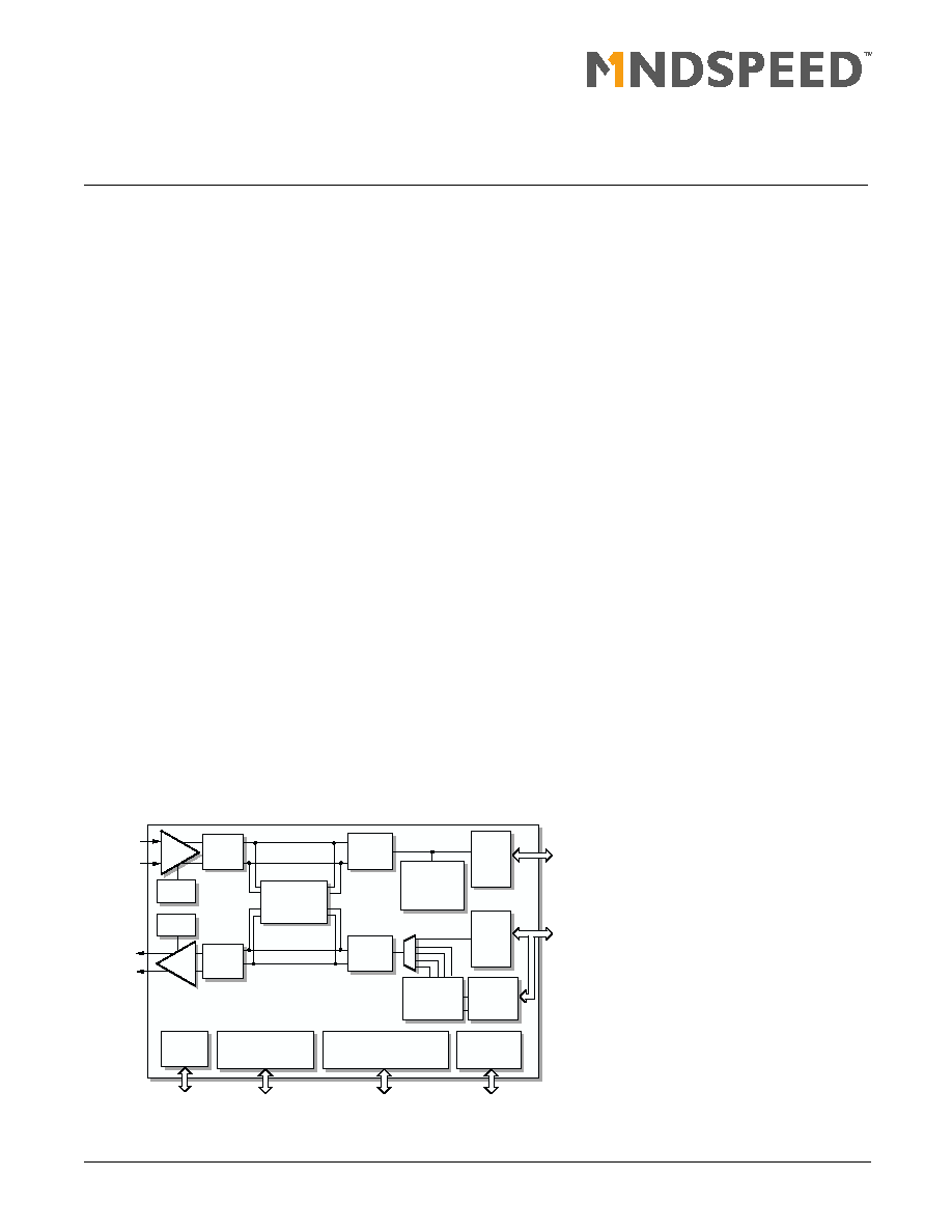
Functional Block Diagram
Distinguishing Features
!
Single-chip T1/E1 framer with short/long
haul physical line interface
!
Frames to popular T1/E1 standards:
"
T1--SF, ESF, SLC
96, T1DM
"
E1--PCM
-
30, G.704, G.706, G.732
ISDN primary rate
!
On-chip physical line interface
compatible with:
"
DSX-1/E1 short haul signals
"
DS-1 (T1.403) and ETSI long haul
signals
!
Two-frame transmit and receive PCM slip
buffers
!
Clock rate adapter synthesizes jitter
attenuated system clocks from an internal
or external reference
!
Parallel 8-bit microprocessor port
supports Intel or Motorola buses
!
Automated Facility Data Link (FDL)
management
!
BERT generation and counting
!
Two full-duplex HDLC controllers for data
link and LAPD/SS7 signaling
!
B8ZS/HDB3/Bit 7 zero suppression
!
80-pin MQFP surface-mount package
!
Operates from a single +5 Vdc ±5% power
supply
!
Low-power CMOS technology
Applications
!
T1/E1 Channel Service Unit/Data Service
Unit (CSU/DSU)
!
Digital Access Cross-Connect Systems
(DACS)
!
T1/E1 Multiplexer (MUX)
!
PBXs and PCM channel bank
!
T1/E1 HDSL terminal unit
!
ISDN Primary Rate Access (PRA)
Receive
System
Bus
Transmit
System
Bus
CLAD I/O
Dual-Rail/NRZ/
Externak DL3
Motorola/Intel
Processor Bus
Test Port
Receive
Analog
Transmit
Analog
T1/E1
Transmit
Framer
TX
Slip
Buffer
RX
Slip
Buffer
T1/E1
Receive
Framer
Overhead
Insertion
Clock Rate
Adaptor
Control/Status
Registers
JTAG
Data Link Controllers
DL1 and DL2
EQ
RPLL
Pulse
LBO
TPLL
TX or RX
Jitter
Attenuator
ZCS
Decode
ZCS
Encode
RX
TX

© 2001, 2002
Mindspeed TechnologiesTM, A Conexant Business
All Rights Reserved.
Information in this document is provided in connection with Mindspeed Technologies ("Mindspeed") products. These materials are provided by
Mindspeed as a service to its customers and may be used for informational purposes only. Mindspeed assumes no responsibility for errors or
omissions in these materials. Mindspeed may make changes to specifications and product descriptions at any time, without notice. Mindspeed
makes no commitment to update the information and shall have no responsibility whatsoever for conflicts or incompatibilities arising from future
changes to its specifications and product descriptions.
No license, express or implied, by estoppel or otherwise, to any intellectual property rights is granted by this document. Except as provided in
Mindspeed's Terms and Conditions of Sale for such products, Mindspeed assumes no liability whatsoever.
THESE MATERIALS ARE PROVIDED "AS IS" WITHOUT WARRANTY OF ANY KIND, EITHER EXPRESS OR IMPLIED, RELATING TO SALE
AND/OR USE OF MINDSPEED PRODUCTS INCLUDING LIABILITY OR WARRANTIES RELATING TO FITNESS FOR A PARTICULAR
PURPOSE, CONSEQUENTIAL OR INCIDENTAL DAMAGES, MERCHANTABILITY, OR INFRINGEMENT OF ANY PATENT, COPYRIGHT OR
OTHER INTELLECTUAL PROPERTY RIGHT. MINDSPEED FURTHER DOES NOT WARRANT THE ACCURACY OR COMPLETENESS OF
THE INFORMATION, TEXT, GRAPHICS OR OTHER ITEMS CONTAINED WITHIN THESE MATERIALS. MINDSPEED SHALL NOT BE
LIABLE FOR ANY SPECIAL, INDIRECT, INCIDENTAL, OR CONSEQUENTIAL DAMAGES, INCLUDING WITHOUT LIMITATION, LOST R
Mindspeed products are not intended for use in medical, lifesaving or life sustaining applications. Mindspeed customers using or selling
Mindspeed products for use in such applications do so at their own risk and agree to fully indemnify Mindspeed for any damages resulting from
such improper use or sale.
The following are trademarks of Conexant Systems, Inc.: Mindspeed TechnologiesTM, the MindspeedTM logo, and "Build It First"TM. Product
names or services listed in this publication are for identification purposes only, and may be trademarks of third parties. Third-party brands and
names are the property of their respective owners.
For additional disclaimer information, please consult Mindspeed Technologies Legal Information posted at
www.mindspeed.com
which is
incorporated by reference.
ii
Mindspeed TechnologiesTM
500030B
Ordering Information
Revision History
Model Number
Package
Operating Temperature
Reduced Features
(1)
Bt8370EPF
80-Pin MQFP
≠40 to 85 ∞C
none
Bt8370KPF
80-Pin MQFP
0 to 70 ∞C
none
Bt8375EPF
80-Pin MQFP
≠40 to 85 ∞C
Short haul
Bt8375KPF
80-Pin MQFP
0 to 70 ∞C
Short haul
Bt8376EPF
80-Pin MQFP
≠40 to 85 ∞C
Short haul; no CLAD output
Bt8376KPF
80-Pin MQFP
0 to 70 ∞C
Short haul; no CLAD output
FOOTNOTE:
(1)
Cost reduced Bt8375 and Bt8376 are pin- and register-compatible versions of Bt8370 with reduced features. Contact the local sales
representative for ordering information and pricing.
Rev
Description
A
Initial release.
B
Technical corrections.
C
Technical corrections.
D
Technical corrections (added changes for Bt8375 and Bt8376).
E
Technical corrections and additions.
A
New document #500030A; formerly document #100051E. Incorporated errata document #500184A in Appendix D
and product bulletin #100679C in the Application chapter. Modified Intel synchronous read and write timing, added
basic configurations in Appendix E, enhanced description of SEF for T1 and E1. Added detailed feature summary.
B
Deleted transmit chip side secondary surge protection blocks in Figures 4-2 and 4-4. Revised part numbers from
Bt28370/75/76 to Bt8370/75/76.

500030B
Mindspeed TechnologiesTM
iii
Bt8370/75/76 Data Sheet
Bt8370EVM--Bt8370 Evaluation Module, Quad T1/E1 ISDN PRI Board
Detailed Feature Summary
Frame Alignment
!
Framed Formats:
"
Independent transmit and receive framing modes
"
T1: FT/SF/ESF/SLC
"
T1DM
"
E1: FAS/MFAS/FAS+CAS/MFAS+CAS
!
Maximum Average Reframe Time (MART) <50 ms
!
Transmitter alignment modes:
"
Align to system bus data
"
Align to system bus sync
"
Align to buffer data (embedded framing)
!
Unframed mode
Signaling
!
T1: 2-,4-, or 16-state, robbed-bit ABCD signaling
!
E1: Channel Associated Signaling (CAS) in any time slot
!
Per-channel receive signaling stack
!
Signaling state change interrupt
!
Automatic and manual signaling freeze
!
Debounce signaling (2-bit integration)
!
Unicode detection
!
Signaling reinsertion on PCM system bus
!
Separate I/O for system bus signaling
!
Per-channel transparent
Clock Rate Adapter
!
Outputs jitter attenuated system bus clock (CLADO) (not available
on Bt8376)
!
Outputs jitter attenuated line rate clock (JCLK)
!
Supports all output clock combinations:
"
JCLK = 1544 k (T1) or 2048 k (E1)
"
CLADO = JCLK x 2
N
, N = 0 to 3
"
CLADO = 1536 k or 2560 k
!
Programmable input timing reference:
"
RXCLK = Recovered Clock
"
TXCLK = Transmit Clock
"
REFCKI = Internal Clock
"
CLADI = Clock Rate Adapter Input
!
Subrate CLADI timing reference:
"
Line rate x (1/2
N
), N = 0 to 8
"
References as low as 8 kHz
Line Interface Unit
!
Short haul interfaces:
"
T1.102-1993
"
G.703 at 1.544 or 2.048 Mbps
"
ITU-T recommendation 1.430
!
ITU-T Recommendation 1.431
!
Long haul interfaces (Bt8370 only):
"
ANSI T1.403-1995 customer-to-network metallic interface
"
Telcordia TR-303 integrated digital loop carrier
An evaluation module is available and provides a convenient platform to test and evaluate Bt8370 performance and features. The Bt8370EVM
provides up to four T1/E1 transceivers, all necessary line interface circuitry for T1 and E1 connections, and a simple RS232 serial user inter-
face for setting device parameters and displaying status information on any VT100-compatible terminal.
Contact the local sales representative for ordering information and pricing.
Bt8370
Local PCM Highway (128 Channel, 8 MHz)
Address
Data Bus
9
8
MC68302
Microprocessor
Bt8370
Bus
T1 or E1 connection at DSX or CSU levels
Bt8370
Bt8370
Bt8370
RS232 User
Interface

iv
Mindspeed TechnologiesTM
500030B
Bt8370/75/76 Data Sheet
!
Analog receive line interface:
"
100/120
load impedance for 19-26 #AWG (0.4≠0.9 mm)
UTP cables
"
75
load impedance for coaxial cable
"
Equalizer compensation for ≠20 or ≠30 dB bridged monitor
levels
"
Analog signal level meter
!
Analog transmit line interface:
"
Pulse shapes for 0≠655 ft., in 133 ft. steps (T1 DSX-1)
"
LBO filters for 0≠22.5 dB, in 7.5 dB steps per FCC Part 68
"
External termination for improved return loss
"
Line driver enable/disable for protection switching
"
Output short circuit protection (for BABT applications)
"
Analog drive level monitor
!
Jitter Attenuator (JAT) elastic store:
"
Receive or transmit direction
"
8-, 16-, 32-, 64-, or 128-bit depth
"
Automatic and manual centering
!
Bipolar Alternate Mark Inversion (AMI) line coding
!
Optional Zero Code Suppression (ZCS):
"
Independent transmit and receive
"
T1: Binary with 8 Zero Substitution (B8ZS)
"
E1: High Density Bipolar of Order 3 (HDB3)
"
T1DM: Unassigned MUX Code (UMC)
"
Per-channel B7ZS
"
Receive ZCS signature detector
"
Pulse density violation monitor/enforcer
!
Analog bypass mode for framer-only or LIU-only applications
Loopbacks
!
Remote loopback towards line
"
With or without JAT
"
Retains BPV transparency
!
Payload loopback
!
Per-channel DSO remote loopback
!
Local loopback towards system
"
Analog line loopback
"
Framer digital loopback
"
Per-channel DSO local loopback
!
Inband loopback code detection/generation
!
Simultaneous local and remote line loopbacks
Processor Interface
!
Parallel 8-bit bus
!
Data strobes (Motorola) or address latch enable (Intel)
!
Multiplexed or non-multiplexed address/data bus
!
Synchronous or asynchronous data transfers
!
36 MHz synchronous without wait states (50 ns access)
!
Open drain interrupt output with maskable sources
Out-of-Service Testing and Maintenance
!
Pseudorandom Bit Sequence (PRBS):
"
Independent transmit and receive
"
2
11
, 2
15
, 2
20
, 2
23
patterns
"
Framed or unframed mode
"
Optional 7/14 zero limit
"
Bit Error Counter (BERR)
!
Single error insertion:
"
PRBS error
"
Framing error
"
CRC error
"
BPV/LCV error
"
COFA error
In-Service Performance Monitoring
!
One-second timer I/O to synchronize reporting
!
Receive error detectors with accumulators:
"
Bipolar/Line Code Violations (LCV)
"
Excessive Zeros (EXZ)
"
Loss of Frame (RLOF)
"
Framing Errors (FERR)
"
CRC Errors (CERR)
"
Far End Block Errors (FEBE)
"
Severely Errored Frames (SEF)
"
Change of Frame Alignment (COFA)
!
Transmit Error Detectors:
"
Loss of Frame (TLOF)
"
Framing errors (TFERR)
"
Multiframe Errors (TMERR)
CRC Errors (TCERR)
"
Loss of Transmit Clock (TLOC)
"
Transmit Short Circuit (TSHORT)
!
Receive alarm detectors:
"
Alarm Indication Signal (AIS)
"
Loss of Signal (RLOS)
"
Loss of Analog Input (RALOS)
"
RAI/Yellow Alarm (YEL)
"
Multiframe Yellow (MYEL)
"
Lost Frame Alignment (FRED)
"
Lost Multiframe Alignment (MRED)
!
Controlled Frame Slip (RFSLIP) Uncontrolled Frame Slip
(RUSLIP)
!
Automatic and on-demand transmit alarms:
"
AIS following RLOS and/or TLOC
"
Automatic AIS clock switching
"
YEL following FRED
"
MYEL following MRED
"
FEBE following CERR

500030B
Mindspeed TechnologiesTM
v
Bt8370/75/76 Data Sheet
System Bus Interface (SBI)
!
System bus data rates:
"
1536 k (T1 without F-bits)
"
1544 k (T1)
"
2048 k (E1)
"
4096 k (2E1)
"
8192 k (4E1)
!
Clock operation at 1x or 2x data rate
!
Selectable I/O clock edges
!
Master, slave, or mixed bus timing
!
Bit and time slot frame sync offsets
!
Bus shares up to four Bt8370/75/76 devices without external
MUX
!
DSO drop/insert indicators for external MUX
!
Embedded T1 framing transport per G.802
!
Receive and transmit slip buffers:
"
Bypass, 2-frame, or 64-bit depth
"
Slip detection with directional status
"
Slip buffer phase status
"
Per-channel idle code insertion
"
Processor-accessible data buffers
!
Direct connection to upper layer devices:
"
Link layer: Bt8071A, Bt8474
"
SMDS layer: Bt8210
"
ATM layer: Bt8215, Bt8222
!
Supported system bus formats:
"
AT&T Concentration Highway Interface (CHI)
"
Multi-Vendor Integration Protocol (MVIP)
"
Mitel S/T
"
H.100
Device Differences Summary
Data Links
!
Two full-featured data link controllers (DL1 and DL2) (Bt8370,
Bt8375) or one data link controller (DL1) (Bt8376):
"
64-octet transmit and receive FIFOs
"
HDLC Message Oriented Protocol (MOP)
"
Unformatted data transfer
"
Unformatted circular buffer
"
End of message/buffer interrupt
"
Near full/empty interrupts at selected depth
!
Access any bit combination in any time slot:
"
ISDN D-channels at 16, 32, or 64 Kbps
"
National/spare bits (SA-bits) in 4 Kbps increments
"
CCS/SS7
"
T1DM R-bits
!
Access T1 F-bits in even, odd, or all frames:
"
Automatic Performance Report Message (PRM) generator
"
ESF Facility Data Link (FDL)
"
Unformatted SLC-96 overhead
"
Bit-Oriented Protocol (BOP) priority code word generation and
detection
!
Separate I/O for external data link (DL3)
Device Differences Summary
Device
Line Interface
Unit
Data Link
Controllers
Clock Rate
Adapter
Bt8370
(Full Featured)
Short haul/
long haul
Two
Controllers
Full Featured
Bt8375
Short haul only Two
Controllers
Full Featured
Bt8376
Short haul only One Controller
No CLAD
Output