Data Sheet
Mindspeed Technologies
TM
28250-DSH-002-A
December
2002
CX28250
ATM Physical Interface (PHY) Devices
The CX28250 is an ATM-SONET Physical Layer (PHY) device with an integrated, PLL
clock and data recovery (CDR) circuit. This device has optimized SONET framer
functions for mapping ATM cells to SONET payloads for edge switch applications, and
optional enhanced feature sets for ATM-WAN access applications. It provides ATM
Forum-compliant service termination, and maps the 53-byte cells from an ATM switch
fabric or an adaptation layer processor (SAR) into the SONET payload. The CX28250
device is tailored to meet a wide variety of ATM OC-3 applications. These include WAN
terminals, ATM LAN and WAN switches, ATM OC-3 NICs, and Ethernet-ATM uplink
cards.
The CX28250 uses an ATM Forum UTOPIA Level 2-compliant host interface designed
for a multi-PHY environment. The ATM framer provides G.804 cell processing, with HEC
generation, checking, and alignment operations. It provides a 155 Mbps SONET
termination with all of the counters needed for capturing both SONET and ATM error
events as specified by the ATM Forum. A proprietary protection scheme allows for
near-instantaneous switching between active and stand-by PHYs.
The CX28250 uses a Pseudo-Emitter Coupled Logic (PECL) line interface compliant
with the ATM Forum's WIRE definition. Thus, designers can connect directly to either
fiber optic or Cat 5 Physical Media Dependant (PMD) devices. For diagnostics, three
loopback modes are provided: source loopback, line loopback before the ATM
processor, and line loopback at the UTOPIA block. In addition, the CX28250 can
generate BIP-8 errors and insert invalid HECs.
The CX28250 supports the following:
�
Compliance with the jitter requirements of Bellcore's GR-253-CORE.
�
Automatic Protection Switching (APS) using the K1/K2 overhead octets and a Bit Error Rate
(BER) integrator.
�
Compatible with Mindspeed CX28297 software driver.
�
Access to the S1 octet for system timing.
�
Data transmission/reception over the Data Link message channels, D1-D3 and D4-D12.
�
Two new input pins have been added: InsPthAIS and InsLnAIS. When asserted high, these
pins cause the CX28250 to generate an AIS in the appropriate overhead.
�
Two new output pins have also been added: LPOut and PFOut. These indicate that an AIS alarm
has been received.
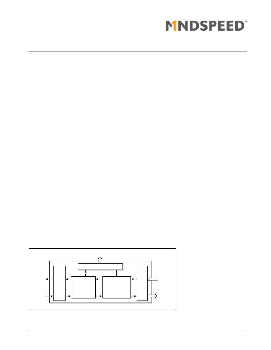
Functional Block Diagram
ATM WIRE
Interface
CX28250
UTOPIA
Level 2
UTOPIA
Level 2
Interface
Microprocessor Interface
SONET Framer and
Overhead Processor
STS-3c/STM-1
(GR-253-CORE)
ATM Formatter
(G.804 Cell Processing)
PMD
Interface
8/16 Bits
8/16 Bits
8 Bits
Clock
Recovery
Tx
4-cell
FIFO
Rx
4-cell
FIFO
Microprocessor Bus
Line
Interface
Host
Interface
500035_001
Distinguishing Features
�
Tested APS software driver available
from Mindspeed
�
Synthesizes a 155.52 MHz clock
from an 19.44 MHz input
�
UTOPIA Level 2 interface
�
Meets ITU, ANSI, and ATM Forum
standards
�
ATM Forum WIRE interface for PMDs
using PECL
�
D1-D3, D4-D12 external data link
�
Supports APS (K1/K2 bytes)
�
Line Fail and Path Fail outputs
�
SRAM-style microprocessor
interface for all control and
configuration registers
�
Glueless interface to the CN823x
segmentation and reassembly
devices
�
JTAG (IEEE 1149.1a-1993) compliant
�
8 kHz and 19.44 MHz selectable sync
outputs
�
SONET overhead processing
�
Automatic collection of one-second
statistics
�
Low power consumption-500 mW
�
3.3 V, (
�
40
�
C to 85
�
C)
�
Package: 156-pin BGA
Applications
�
Switches, Hubs, Routers
�
LAN NIC cards
�
DSLAM uplinks
Line Interface
�
ATM Forum WIRE interface
specification compliant
�
PECL I/O, compatible with PMD
optical and UTP interface devices
�
Clock recovery from NRZ input data
�
Recovery of receive-octet alignment
and octet clock from F6/28 framing
pattern
�
Select transmit clock from input or
recovered receive clock

28250-DSH-002-A
Mindspeed Technologies
TM
� 2002, 2003
Mindspeed Technologies Inc., a Delaware Corporation ("Mindspeed TM")
All Rights Reserved.
Information in this document is provided in connection with products of Mindspeed Technologies ("Mindspeed"). These materials are
provided by Mindspeed as a service to its customers and may be used for informational purposes only. Mindspeed assumes no
responsibility for errors or omissions in these materials. Mindspeed may make changes to specifications and product descriptions at
any time, without notice. Mindspeed makes no commitment to update the information and shall have no responsibility whatsoever for
conflicts or incompatibilities arising from future changes to its specifications and product descriptions.
No license, express or implied, by estoppel or otherwise, to any intellectual property rights is granted by this document. In the event of
a conflict between the terms contained herein and those of any applicable agreement ("Agreement") governing the sale of
Mindspeed's products (including without limitation Mindspeed's Terms and Conditions of Sale) the terms of such Agreement shall
control.
THESE MATERIALS ARE PROVIDED "AS IS" WITHOUT WARRANTY OF ANY KIND, EITHER EXPRESS OR IMPLIED, RELATING
TO SALE AND/OR USE OF MINDSPEED PRODUCTS INCLUDING LIABILITY OR WARRANTIES RELATING TO FITNESS FOR A
PARTICULAR PURPOSE, CONSEQUENTIAL OR INCIDENTAL DAMAGES, MERCHANTABILITY, OR INFRINGEMENT OF ANY
PATENT, COPYRIGHT OR OTHER INTELLECTUAL PROPERTY RIGHT. MINDSPEED FURTHER DOES NOT WARRANT THE
ACCURACY OR COMPLETENESS OF THE INFORMATION, TEXT, GRAPHICS OR OTHER ITEMS CONTAINED WITHIN THESE
MATERIALS. MINDSPEED SHALL NOT BE LIABLE FOR ANY DAMAGES WHICH MAY RESULT FROM THE USE OF THESE
MATERIALS.
Mindspeed products are not intended for use in medical, lifesaving or life sustaining applications. Mindspeed customers using or
selling Mindspeed products for use in such applications do so at their own risk and agree to fully indemnify Mindspeed for any
damages resulting from such improper use or sale.
The following are trademarks of Mindspeed TechnologiesTM, the MindspeedTM logo, and "Build It First"TM. Product names or services
listed in this publication are for identification purposes only, and may be trademarks of third parties. Third-party brands and names are
the property of their respective owners.
Mindspeed Product Definitions
A "Chip" is an integrated circuit, a piece of silicon or other semiconductor on which is etched or imprinted a network of electronic
components such as transistors, diodes, resistors, etc. and their interconnections, which is fully assembled with packaging providing
pins for connection to other circuits or systems.
A "Die" is an unassembled integrated circuit manufactured from a semiconductor material without packaging or pins for connections
to other circuits or systems. Dies may be shipped on a wafer separated from each other by scribe lines, or they may be cut,
separated and placed into appropriate packaging for shipping.
"Board-level Products" are larger electrical circuits that are set out on a board containing one or more Chips and circuitry to perform
a specialized function.
"Software Products" shall mean all software, in executable code, that is embedded, bundled or included with Chips or Die.
A "Prototype" Product is a Chip or Die that has just begun the qualification process. It is marked with a capital "P" at the end of its
unique part number.
"Pre-production" Products are Chips or Die that have not completed the qualification process but have results from some of the
qualification tests. Such Products are marked with a capital "R" at the end of their unique part number.
A "Production" Product is a Chip or Die that is fully qualified and has no letter marked at the end of its unique part number.
A "Sample" Product is any Product that a Buyer may sample, in any stage of qualification, in small numbers. All such sample
Products shall be noted as such on an acknowledgment, invoice, shipping document or other writing issued by Seller.
Ordering Information

28250-DSH-002-A
Mindspeed Technologies
TM
SONET Framer Functions
�
Recovers frame location using F6/28 framing pattern
�
Processes pointer to locate payload envelope
�
Provides Out-of-Frame (OOF), Loss-of-Pointer (LOP), and
Alarm Indication Status (AIS) status
�
Provides frame and payload position information to other
blocks
�
Generates clocks and frame counters
�
Maps cell data into payload envelope
�
Generates all section, line, and path overhead and alarms
�
Performs cell and frame scrambling before transmission
�
Detects and integrates alarms for reporting in status
registers
�
Detects BIP and Remote Error Indication (REI) errors for
error counters
�
Recovers D1-D3 and D4-D12 data link
Cell Alignment Framing Section
�
Recovers cell alignment from HEC
�
Performs HEC error correction
�
Strobes and cell sync for UTOPIA interface
�
Generates cell status bits, cell counts, and error counts
�
Reads cell data from the UTOPIA FIFO
�
Inserts headers and generates HEC
�
Inserts idle cells when no traffic is ready
Microprocessor Interface
�
SRAM-like interface mode with high-performance or
low-power access selection
�
Glueless CN823x SAR interface mode
�
8-bit data bus
�
Open-drain interrupt output
Support for Automatic Protection Switching (APS)
�
APS driver source code available from Mindspeed.
�
Register control allows for support of APS
�
Software support:
� CX28297 Device Driver
� CX28299 APS Driver
�
K1/K2 Transmit control register allows transmission of any
value
�
Separate control bits for AIS, line REI
�
K1/K2 receive status register allows observation of incoming
octet values
�
Maskable interrupt on any change in received value
�
Software interrupt routine can easily implement APS
protocol
�
Signal Fail/Signal Detect BER threshold monitoring
�
Line Fail and Path Fail hardware outputs
�
Line AIS and Path AIS can be generated by hardware input
pins
Counters/Status and Interrupt Registers
�
Summary interrupt indications
�
Configuration of interrupt enables
�
One-second status latching
�
One-second counter latching
�
Eight general purpose outputs, configurable as status
indicator pins
The following diagram is a Network Interface Card (NIC) application of the CX28250
500035_002
CX28250
CN8234/CN8236
SRAM
Fiber
or
Cat 5
PCI
Bus
PMD
Interface
UTOPIA Bus
Interface
Local Bus
Interface
PCI
Interface
UTOPIA
Interface
Microprocessor
Interface
UTOPIA Bus
Local Bus
Note(s):
1. The CN8234 SAR has an 8 bit UTOPIA level 1 interface.
2. The CN8236 SAR has a 8/16 bit UTOPIA level 1/2 interface and supports multi-PHY operation.

28250-DSH-002-A
Mindspeed Technologies
TM
Line Interface (continued)
�
PMD (line) and Framer (source) loopbacks for diagnostic
testing
�
Loss of Signal (LOS) detection
�
19.44 MHz reference clock
UTOPIA Level 2 Interface
�
PHY cell to UTOPIA interface
�
50 MHz maximum data rate
�
8/16-bit data path interface
�
Multi-PHY support
�
Mode-compatible with UTOPIA level 1
�
Configurable cell buffer depth
SONET STS-3c/STM-1 Framer
Section Overhead Octets Supported
Line Overhead Octets Supported
Path Overhead Octets Supported
Transmit
Receive
A1/A2
F6/28 hex or disable 00
Monitor out of frame state machine
J0
01 hex or 64-byte trace buffer
Monitor Rx trace buffer, interrupt on change
Z0
1
, Z0
2
02, 03 hex/user defined
Not checked
B1
Calculated, error insertion
Checked, errors counted
D1, D2, D3
00 hex or external data link
External data link
Transmit
Receive
H1/H2
620A/93FF hex pointer
Full GR.253 pointer processor
H3
Set to 00
Used in pointer processor
B2
Calculated, error insertion
Checked, errors counted
K1/K2
Insertable via register
Checked, interrupt on change
D4-D12
00 hex or external data link
External data link
S1
Insertable via register
Checked, interrupt on change
M1
Line
REI
inserted
Checked, errors counted
Transmit
Receive
J1
00 hex or 64-byte trace buffer
Monitor Rx trace buffer, interrupt on change
B3
Calculated, error insertion
Checked, errors counted
C2
13 hex for ATM mapping
Checked for 01 or 13 hex
G1
Path
REI
, RDI inserted
Checked, errors counted, status
Z2
Monitored