
Features - 4
Terminal Descriptions - 5
Specification Tables - 7
Functional Description - 17
Register Information - 21
Package Information - 29
World Wide Sales Companies - 38
M21120
34 x 34 3.2 Gbps Crosspoint Switch with Input Equalization
Data Sheet
21120-DSH-001-B, 3/27/03
Mindspeed TechnologiesTM

M21120
34 x 34 3.2 Gbps Crosspoint Switch with Input Equalization
21120-DSH-001-B, 3/27/03
Page 2 of 38
Mindspeed TechnologiesTM
Contents
Features . . . . . . . . . . . . . . . . . . . . . . . . . . . . . . . . . . . . . . . . . . . . . . . . . . . . . . . . . . . . . . . . . . . . . . . . . . . . . 4
General Description. . . . . . . . . . . . . . . . . . . . . . . . . . . . . . . . . . . . . . . . . . . . . . . . . . . . . . . . . . . . . . . . . . . . . 4
Applications . . . . . . . . . . . . . . . . . . . . . . . . . . . . . . . . . . . . . . . . . . . . . . . . . . . . . . . . . . . . . . . . . . . . . . . . . . . 4
Ordering Information . . . . . . . . . . . . . . . . . . . . . . . . . . . . . . . . . . . . . . . . . . . . . . . . . . . . . . . . . . . . . . . . . . . . 4
Figure 1. Jitter Removal by Input Equalization . . . . . . . . . . . . . . . . . . . . . . . . . . . . . . . . . . . . . . . . . . . . . . . 4
Figure 2. M21120 Crosspoint Switch Functional Block Diagram . . . . . . . . . . . . . . . . . . . . . . . . . . . . . . . . . 5
Table 1. Terminal Functional Descriptions(4) . . . . . . . . . . . . . . . . . . . . . . . . . . . . . . . . . . . . . . . . . . . . . . . . 5
Table 2. High-speed PCML RF Electrical Specifications (1) . . . . . . . . . . . . . . . . . . . . . . . . . . . . . . . . . . . . . 7
Table 3. +3.3V CMOS DC Electrical Specifications (1) (2) (3) . . . . . . . . . . . . . . . . . . . . . . . . . . . . . . . . . . . 8
Table 4. +2.5V CMOS DC Electrical Specifications (1)(2) . . . . . . . . . . . . . . . . . . . . . . . . . . . . . . . . . . . . . . 8
Table 5. +3.3V PCML DC Electrical Specifications (1) . . . . . . . . . . . . . . . . . . . . . . . . . . . . . . . . . . . . . . . . . 8
Table 6. +2.5 V PCML DC Electrical Specifications (1). . . . . . . . . . . . . . . . . . . . . . . . . . . . . . . . . . . . . . . . . 9
Table 7. Recommended Operating Conditions . . . . . . . . . . . . . . . . . . . . . . . . . . . . . . . . . . . . . . . . . . . . . . 10
Table 8. Power DC Electrical Specifications (1)(2) . . . . . . . . . . . . . . . . . . . . . . . . . . . . . . . . . . . . . . . . . . . 10
Table 9. Absolute Maximum Ratings (1) . . . . . . . . . . . . . . . . . . . . . . . . . . . . . . . . . . . . . . . . . . . . . . . . . . . 11
Serial Interface and Switch Programming . . . . . . . . . . . . . . . . . . . . . . . . . . . . . . . . . . . . . . . . . . . . . . . . . . . 12
Introduction . . . . . . . . . . . . . . . . . . . . . . . . . . . . . . . . . . . . . . . . . . . . . . . . . . . . . . . . . . . . . . . . . . . . . . . . . . 12
Register Concept . . . . . . . . . . . . . . . . . . . . . . . . . . . . . . . . . . . . . . . . . . . . . . . . . . . . . . . . . . . . . . . . . . . . . 12
Switch State Register Concept. . . . . . . . . . . . . . . . . . . . . . . . . . . . . . . . . . . . . . . . . . . . . . . . . . . . . . . . . . . 12
Figure 3. Parallel Write Timing Diagram . . . . . . . . . . . . . . . . . . . . . . . . . . . . . . . . . . . . . . . . . . . . . . . . . . . 13
Figure 4. Parallel Read Timing Diagram . . . . . . . . . . . . . . . . . . . . . . . . . . . . . . . . . . . . . . . . . . . . . . . . . . . 13
Table 10. Parallel Timing Specifications For Write Operations . . . . . . . . . . . . . . . . . . . . . . . . . . . . . . . . . . 14
Table 11. Parallel TIming Specifications For Read Operations . . . . . . . . . . . . . . . . . . . . . . . . . . . . . . . . . . 14
Parallel I/O Overview. . . . . . . . . . . . . . . . . . . . . . . . . . . . . . . . . . . . . . . . . . . . . . . . . . . . . . . . . . . . . . . . . . . 15
Serial I/O Overview . . . . . . . . . . . . . . . . . . . . . . . . . . . . . . . . . . . . . . . . . . . . . . . . . . . . . . . . . . . . . . . . . . . 15
Figure 5. Serial Word Format . . . . . . . . . . . . . . . . . . . . . . . . . . . . . . . . . . . . . . . . . . . . . . . . . . . . . . . . . . . 15
Figure 6. Serial Write Mode. . . . . . . . . . . . . . . . . . . . . . . . . . . . . . . . . . . . . . . . . . . . . . . . . . . . . . . . . . . . . 15
Figure 7. Serial Read Mode . . . . . . . . . . . . . . . . . . . . . . . . . . . . . . . . . . . . . . . . . . . . . . . . . . . . . . . . . . . . 16
Table 12. Serial Interface Timing � Specified at Recommended Operating Conditions . . . . . . . . . . . . . . . 16
Switch Function Details . . . . . . . . . . . . . . . . . . . . . . . . . . . . . . . . . . . . . . . . . . . . . . . . . . . . . . . . . . . . . . . . . 17

M21120
34 x 34 3.2 Gbps Crosspoint Switch with Input Equalization
21120-DSH-001-B, 3/27/03
Page 3 of 38
Mindspeed TechnologiesTM
Introduction . . . . . . . . . . . . . . . . . . . . . . . . . . . . . . . . . . . . . . . . . . . . . . . . . . . . . . . . . . . . . . . . . . . . . . . . . . 17
Input Equalization . . . . . . . . . . . . . . . . . . . . . . . . . . . . . . . . . . . . . . . . . . . . . . . . . . . . . . . . . . . . . . . . . . . . . 17
Switch Setting . . . . . . . . . . . . . . . . . . . . . . . . . . . . . . . . . . . . . . . . . . . . . . . . . . . . . . . . . . . . . . . . . . . . . . . . 17
Input/Output Enable . . . . . . . . . . . . . . . . . . . . . . . . . . . . . . . . . . . . . . . . . . . . . . . . . . . . . . . . . . . . . . . . . . . 17
xRST/xTEST . . . . . . . . . . . . . . . . . . . . . . . . . . . . . . . . . . . . . . . . . . . . . . . . . . . . . . . . . . . . . . . . . . . . . . . . . 17
Initialization Sequence . . . . . . . . . . . . . . . . . . . . . . . . . . . . . . . . . . . . . . . . . . . . . . . . . . . . . . . . . . . . . . . . . 18
Table 13. Bit Function for Individual Channel Enable Registers (1) . . . . . . . . . . . . . . . . . . . . . . . . . . . . . . 18
Revision Code . . . . . . . . . . . . . . . . . . . . . . . . . . . . . . . . . . . . . . . . . . . . . . . . . . . . . . . . . . . . . . . . . . . . . . . . 20
PRBS TX and RX . . . . . . . . . . . . . . . . . . . . . . . . . . . . . . . . . . . . . . . . . . . . . . . . . . . . . . . . . . . . . . . . . . . . . 20
Figure 8. PRBS Receiver Timing . . . . . . . . . . . . . . . . . . . . . . . . . . . . . . . . . . . . . . . . . . . . . . . . . . . . . . . . 20
Table 14. PRBS Receiver Timing . . . . . . . . . . . . . . . . . . . . . . . . . . . . . . . . . . . . . . . . . . . . . . . . . . . . . . . . 20
Core Power Saving . . . . . . . . . . . . . . . . . . . . . . . . . . . . . . . . . . . . . . . . . . . . . . . . . . . . . . . . . . . . . . . . . . . . 21
Digital Slope Control . . . . . . . . . . . . . . . . . . . . . . . . . . . . . . . . . . . . . . . . . . . . . . . . . . . . . . . . . . . . . . . . . . . 21
Registers . . . . . . . . . . . . . . . . . . . . . . . . . . . . . . . . . . . . . . . . . . . . . . . . . . . . . . . . . . . . . . . . . . . . . . . . . . . . 21
Table 15. Input Channel Number Offsets for Programming Input Channel Selection Registers (00�21h) . 22
Table 16. Register Summary (1) (2) . . . . . . . . . . . . . . . . . . . . . . . . . . . . . . . . . . . . . . . . . . . . . . . . . . . . . 23
Table 17. Register Description . . . . . . . . . . . . . . . . . . . . . . . . . . . . . . . . . . . . . . . . . . . . . . . . . . . . . . . . . . 25
Package Information . . . . . . . . . . . . . . . . . . . . . . . . . . . . . . . . . . . . . . . . . . . . . . . . . . . . . . . . . . . . . . . . . . . 29
Figure 9. Package Dimensions . . . . . . . . . . . . . . . . . . . . . . . . . . . . . . . . . . . . . . . . . . . . . . . . . . . . . . . . . . 29
Figure 10. Package Cross Section . . . . . . . . . . . . . . . . . . . . . . . . . . . . . . . . . . . . . . . . . . . . . . . . . . . . . . . 29
Figure 11. Package Bottom View with Ball Assignments . . . . . . . . . . . . . . . . . . . . . . . . . . . . . . . . . . . . . . 30
Table 18. Ball List Sorted by Ball Location . . . . . . . . . . . . . . . . . . . . . . . . . . . . . . . . . . . . . . . . . . . . . . . . . 31
Table 19. Ball List Sorted by Ball Name . . . . . . . . . . . . . . . . . . . . . . . . . . . . . . . . . . . . . . . . . . . . . . . . . . . 34
Revision History . . . . . . . . . . . . . . . . . . . . . . . . . . . . . . . . . . . . . . . . . . . . . . . . . . . . . . . . . . . . . . . . . . . . . . 39
M21120
34 x 34 3.2 Gbps Crosspoint Switch with Input Equalization
21120-DSH-001-B, 3/27/03
Page 4 of 38
Mindspeed TechnologiesTM
Features
Low power consumption of 4 Watts at 2.5 V
Input equalizer on each channel to reduce deterministic
jitter (ISI), caused by board traces and cables (see
Figure 1
)
Supports any data rate from DC to 3.2 Gbps
Built-in PRBS Tx/Rx for system diagnostics
PowerScaler
TM
for further power reduction based on sys-
tem needs
High-isolation design for low crosstalk jitter
Differential/single-ended high-speed data input/output
Non-blocking and broadcastable
General Description
The M21120, designed for today's demanding telecom and
datacom applications, is a low-power BiCMOS, high-speed
34 x 34 crosspoint switch with input equalization and built-in
system test features.
The device consumes as low as 4 Watts of power (typical at
2.5 V) with all channels operational. In addition, the PowerSca-
ler
TM
features offer dynamically scalable switch settings to fur-
ther reduce power consumption. Unused portions of the core
can be automatically (SmartPower
TM
) turned off, without affect-
ing the operation of the remaining channels.
To improve signal quality, each input buffer is preceded by an
input equalizer (IE), which removes ISI jitter that is usually
caused by PCB skin effect losses. The IE circuit opens the input
data eye in applications where long PCB traces and cables are
used. The input equalizer can be enabled on a per channel ba-
sis.
The device supports data rates from 0 to 3.2 Gbps on each
channel, allowing any combination of SONET, Fibre Channel
(1x, 2x, 10x), InfiniBand, Gigabit Ethernet, and 10 Gbps Ether-
net traffic.
Built-in system test features simplify design, verification, and
production testing of the system. The switch includes an on-
board 2
n
�1 pseudo-random bit sequence transmitter (PRBS
TX) and receiver (PRBS RX).
The M21120 is a non-blocking switch, with multi-cast and
broadcast abilities.
All inputs and outputs are differential PCML (positive current
mode logic) with 2.5 V or 3.3 V supply.
Applications
DWDM Switches
Fiber-optic Telecom Systems (OC-48/OC-48 FEC)
Telecom & Datacom Switches
Storage Area Network (SAN) Switches (Fibre Channel,
2x Fibre Channel, and 10x Fibre Channel)
10 GbE parallel, GbE, and Infiniband networks
Packet Switching
High-speed Automated Test Equipment
The M21120 is available in a 580-terminal, 35 mm, CDBGA
(Cavity Down Ball Grid Array) package, with a case tempera-
ture range of 0 �C to 85 �C, as shown in
Figure 9
and
Figure 10
.
Terminal functional descriptions are listed in
Table 1
. Electrical
specifications are listed in
Table 2
through
Table 12
.
Figure 1
shows jitter removal using input equalization. The
M21120 functional block diagram is illustrated in
Figure 2
.
Ordering Information
Part Number
Package Type
M21120
580-terminal, 35 mm, CDBGA
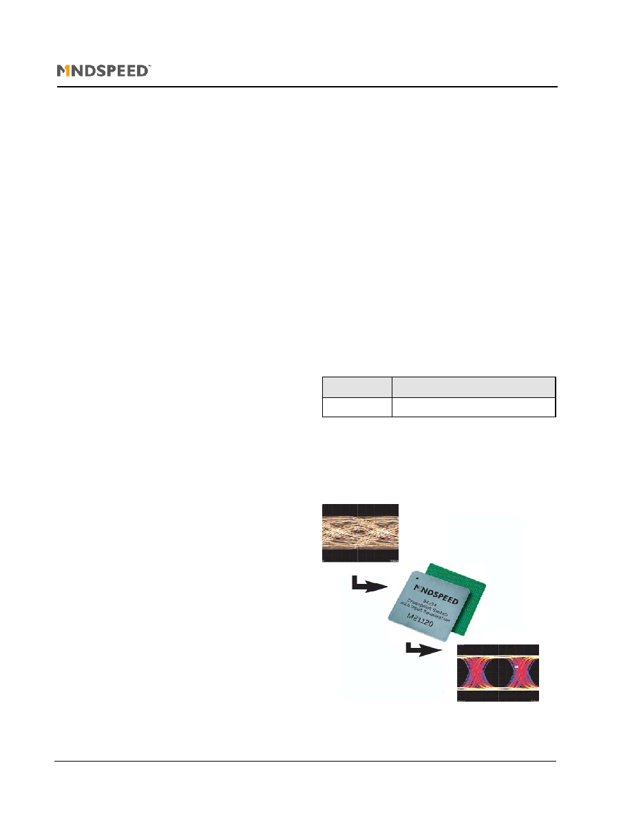
Figure 1. Jitter Removal by Input Equalization
Figure 1a, left, illustrates the
effect of 70" of stripline on a
clean 2.5 Gbps signal.
Figure 1b, below,
illustrates input
equalizer
reduction of ISI
jitter.

M21120
34 x 34 3.2 Gbps Crosspoint Switch with Input Equalization
21120-DSH-001-B, 3/27/03
Page 5 of 38
Mindspeed TechnologiesTM
Figure 2. M21120 Crosspoint Switch Functional Block Diagram
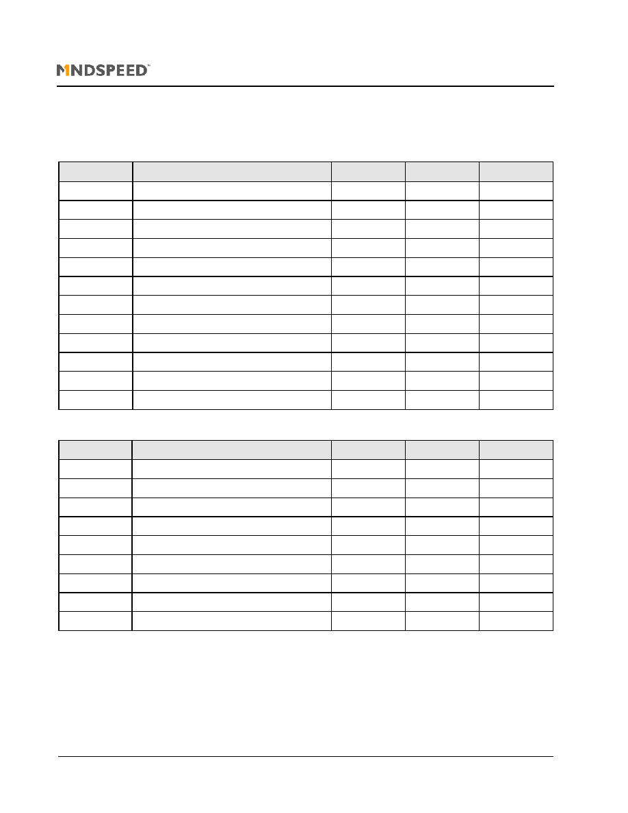
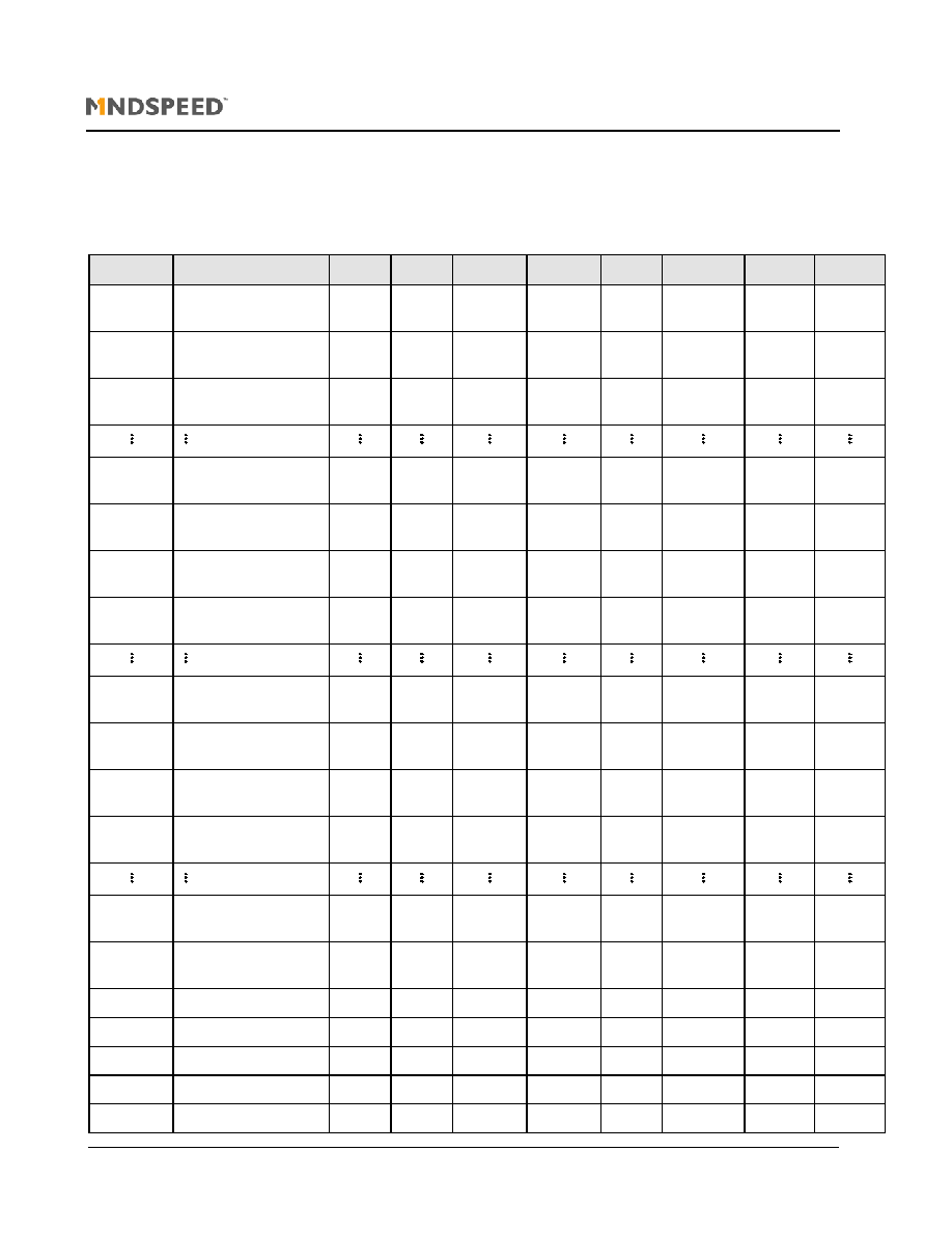
Table 1. Terminal Functional Descriptions
(4)
(Sheet 1 of 2)
Name
Function
Notes
Type
Signal
Input/Output Signals
inp[0:33]
Positive differential high-speed input data
1
I
PCML
inn[0:33]
Negative differential high-speed input data
1
I
PCML
outp[0:33]
Positive differential high-speed output data
�
O
PCML
outn[0:33]
Negative differential high-speed output data
�
O
PCML
xindis
Hardware disable of all Inputs (active low, with internal pulldowns)
�
I
CMOS
xoutdis
Hardware disable of all outputs (active low, with internal pulldowns)
�
I
CMOS
a[7:0]
8 Bit parallel address (bit-7: MSB, bit-0: LSB)
�
I
CMOS
d[5:0]
6 low bits of 8-bit parallel data (bit-0: LSB)
�
I/O
CMOS
d[6]/di
7th bit of parallel data / serial data input
�
I/O
CMOS
d[7]/do
8th bit of parallel data (MSB) / serial data output
�
I/O
CMOS
Hardware Control
r/xw
Parallel I/0: H = read, L = write
�
I
CMOS
xds/sclk
Parallel I/0: data latch, serial I/0: serial clock (hysteresis)
�
I
CMOS
inp/n[33]
Active Configuration
Latch
(slave FF bank)
Input Configuration
Latch
(master FF bank)
Parallel
Serial I/0
and
General
Registers
xset
Data Decode
Data
Write
Data
Read
a[7:0]
d[5:0]
r/xw
d[6]/di
d[7]/do
xds/sclk
ser/xpar
xcs
xrst
xtest
clktxp/n
PRBS
TX
2
n
-1
xentx
dotxp/n
trig
PRBS
RX
2
n
-1
perror
xrstrx
xenrx
clkrxp/n
dirxp/n
Counter
FF
xindis
34 x 34
Differential
Crosspoint
68
Output
Buffer
(PCML)
inp/n[0]
inp/n[1]
outp/n[0]
outp/n[1]
68
Input
Buffer
(PCML)
outp/n[33]
xoutdis
Differential I/O
Single-ended I/O
Legend
Equalization

M21120
34 x 34 3.2 Gbps Crosspoint Switch with Input Equalization
21120-DSH-001-B, 3/27/03
Page 6 of 38
Mindspeed TechnologiesTM
xcs
Serial/parallel: active low I/O enable
�
I
CMOS
ser/xpar
Serial/parallel I/O select: H = serial, L = parallel
�
I
CMOS
xrst
Hardware reset (active low)
�
I
CMOS
xtest
Mindspeed Technologies test pin (active low)
�
I
CMOS
xset
xSET pin (active low) to switch more then one channel at once
�
I
CMOS
dotxp
Positive differential data for 2n-1 pseudorandom signal generator
�
O
PCML
dotxn
Negative differential data for 2n-1 pseudorandom signal generator
�
O
PCML
clktxp
Positive differential clock for 2n-1 pseudorandom signal generator
1
I
PCML
clktxn
Negative differential clock for 2n-1 pseudorandom signal generator
1
I
PCML
xentx
Enable 2n-1 pseudorandom signal generator clock
�
I
CMOS
trig
CLKTX/16 for use as a scope trigger
3
O
PCML
dirxp
Positive differential data for 2n-1 pseudorandom signal receiver
1
I
PCML
dirxn
Negative differential data for 2n-1 pseudorandom signal receiver
1
I
PCML
clkrxp
Positive differential clock for 2n-1 pseudorandom signal receiver
1
I
PCML
clkrxn
Negative differential clock for 2n-1 pseudorandom signal receiver
1
I
PCML
xenrx
Enable 2n-1 pseudorandom RX clock/data (active low)
�
I
CMOS
xrstrx
PRBS Rx reset (active low)
�
O
CMOS
perror
Receiver bit error flag: latches H on first error
�
I
CMOS
Analog and Digital Power
aoutv
DD
Positive supply for crosspoint output drivers
2
P
PWR
aoutv
SS
Negative supply for crosspoint output drivers
2
P
PWR
ainv
DD
Positive supply for crosspoint core, input, and PRBS
2
P
PWR
ainv
SS
Negative supply for crosspoint core, input, and PRBS
2
P
PWR
dv
DD
Positive supply for digital control
2
P
PWR
dv
SS
Negative supply for digital control
2
P
PWR
Notes:
1. Higher input sensitivity and common-mode range over standard PECL.
2. Analog supplies on separate plane in packages; digital supplies do not use package planes.
3. Trig output has a voltage swing of 150 mV peak-to-peak.
4. Internal pull-up resistors on all CMOS inputs unless otherwise noted.
Table 1. Terminal Functional Descriptions
(4)
(Sheet 2 of 2)
Name
Function
Notes
Type
Signal

M21120
34 x 34 3.2 Gbps Crosspoint Switch with Input Equalization
21120-DSH-001-B, 3/27/03
Page 7 of 38
Mindspeed TechnologiesTM
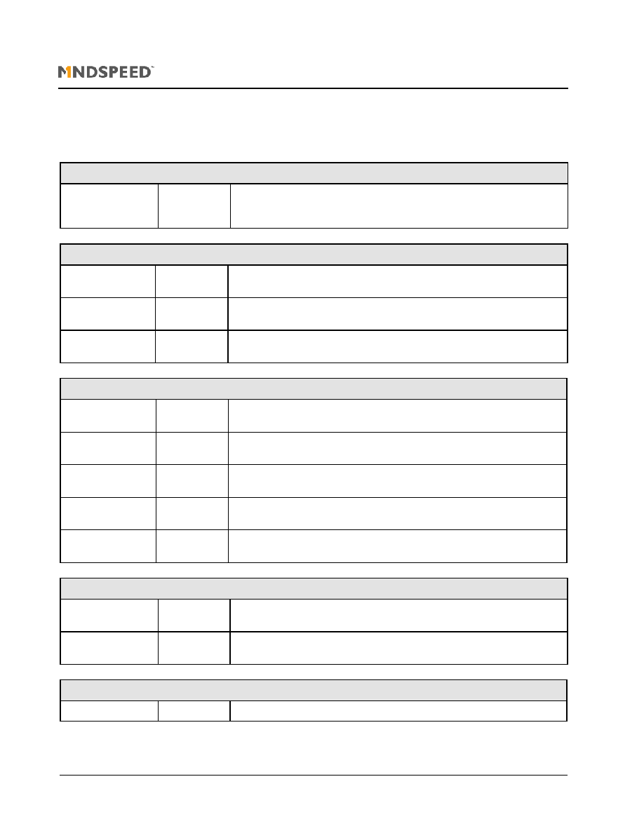
Table 2. High-speed PCML RF Electrical Specifications
(1)
Parameter
Notes
Minimum
Typical
Maximum
Units
Input bit rate (NRZ data)
0
--
3.2
Gbps
Total (random + deterministic) Output jitter (single channel
input only) (RMS)
--
--
7.2
ps
Total (random + deterministic) Output jitter (single channel
input only) (peak-to-peak)
--
--
43
ps
Total (random+ deterministic) Output jitter with 33 interfer-
ing channels (RMS)
--
--
7.7
ps
Total (random + deterministic) Output jitter with 33 interfer-
ing channels (peak-to-peak)
--
--
46
ps
Rise time/fall time (20 to 80 %)
--
75
120
ps
Output return loss (40 MHz to 2.5 GHz)
2, 3
--
�15
--
dB
Output return loss (2.5 GHz to 5 GHz)
2, 3
--
�5
--
dB
Input return loss (40 MHz to 2.5 GHz)
2, 3
--
�15
--
dB
Input return loss (2.5 GHz to 5 GHz)
2, 3
--
�5
--
dB
Notes:
1. Recommended operating condition--see
Table 7
.
2. Input/output return loss typical performance.
3. RF parameters measured into a 50
load.
M21120
34 x 34 3.2 Gbps Crosspoint Switch with Input Equalization
21120-DSH-001-B, 3/27/03
Page 8 of 38
Mindspeed TechnologiesTM
Table 3. +3.3V CMOS DC Electrical Specifications
(1)
(2)
(3)
Symbol
Item
Minimum
Typical
Maximum
Units
V
OH
Output logic high I
OH
= �100
�A
2.9
3.3
--
V
V
OL
Output logic low I
OL
= 100
�A
--
0.0
0.05
V
V
IH
Input logic high
2.0
--
V
DD
V
V
IL
Input logic low
V
SS
� 0.3
--
0.8
V
I
IH
Input current (logic high)
�200
--
200
�A
I
IL
Input current (logic low)
�200
--
200
�A
Notes:
1. Recommended operating condition�see
Table 7
.
2. 50 K
internal pull-ups on all CMOS inputs unless noted as pull-downs.
3. CMOS I/O's are TTL compatible, when the device is powered wth 3.3 V.
Table 4. +2.5V CMOS DC Electrical Specifications
(1)(2)
Symbol
Item
Minimum
Typical
Maximum
Units
V
OH
Output logic high I
OH
= �100
�A
2.3
2.45
--
V
V
OL
Output logic low I
OL
= 100
�A
--
0.0
0.05
V
V
IH
Input logic high
2.0
--
V
DD
V
V
IL
Input logic low
V
SS
� 0.3
--
0.8
V
I
IH
Input current (logic high)
�200
--
200
�A
I
IL
Input current (logic low)
�200
--
200
�A
Notes:
1. Recommended operating conditions--see
Table 7
.
2. 50 K
internal pull-ups on all CMOS inputs unless noted as pull-downs.
Table 5. +3.3V PCML DC Electrical Specifications
(1)
Parameter
Notes
Minimum
Typical
Maximum
Units
Input differential voltage (peak-to-peak)
2, 5
100
--
1200
mV
Input common-mode voltage
3, 5
V
DD
�500
--
V
DD
+100
mV
Differential output voltage (peak-to-peak)
4
750
--
950
mV
Maximum input high voltage
5
--
--
V
DD
+300
mV
Minimum input low voltage
5
V
DD
�800
--
--
mV
Output logic high
V
DD
�35
--
V
DD
mV
M21120
34 x 34 3.2 Gbps Crosspoint Switch with Input Equalization
21120-DSH-001-B, 3/27/03
Page 9 of 38
Mindspeed TechnologiesTM
Output logic low
V
DD
�520
--
V
DD
�410
mV
Notes:
1. Recommended operating condition--see
Table 7
.
2. Example 1200 mV
P-P
differential = 600 mV
P-P
for each single-ended terminal.
3. Common mode is defined as DC voltage shift on AC signal (actual values set after initial simulation).
4. Designed for DC coupled PCML or AC coupled CML, PECL, and ECL (ECL may require off-chip termination).
5. Input differential voltage and input common-mode voltage is constrained by the max./min. input voltages.
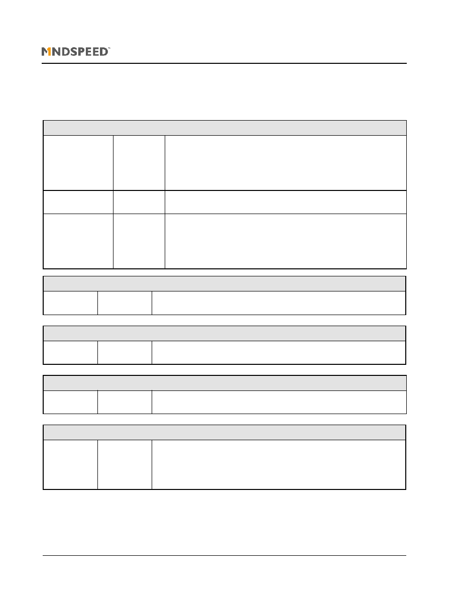
Table 6. +2.5 V PCML DC Electrical Specifications
(1)
Parameter
Notes
Minimum
Typical
Maximum
Units
Input differential voltage (peak-to-peak)
2, 5
100
--
1200
mV
Input Common-mode Voltage
3, 5
V
DD
- 500
--
V
DD
+ 100
mV
Differential Output Voltage (peak-to-peak)
4
700.0
--
900.0
mV
Maximum input high voltage
5
--
--
V
DD
+300
mV
Minimum input low voltage
5
V
DD
�800
--
--
mV
Output Logic High
--
V
DD
- 35
--
V
DD
mV
Output Logic Low
--
V
DD
- 470
--
V
DD
- 385
mV
Notes:
1. Recommended operating conditions - see
Table 7
.
2. Example 1200 mV differential peak-to-peak translates to 600 mV peak-to-peak for each single-ended terminal.
3. Common mode is defined as the DC voltage offset on an AC signal.
4. Designed for DC coupled PCML or AC coupled CML, PECL, ECL (ECL may require off-chip attenuation).
5. Input differential voltage and input common-mode voltage is constrained by the max/min input voltages.
Table 5. +3.3V PCML DC Electrical Specifications
(1)
Parameter
Notes
Minimum
Typical
Maximum
Units
M21120
34 x 34 3.2 Gbps Crosspoint Switch with Input Equalization
21120-DSH-001-B, 3/27/03
Page 10 of 38
Mindspeed TechnologiesTM
Table 7. Recommended Operating Conditions
Parameter
Notes
Symbol
Minimum
Typical
Maximum
Units
Core supply voltage
1
ainv
DD
2.375
2.5/3.3
3.6
V
Output supply voltage
1
aoutv
DD
2.375
2.5/3.3
3.6
V
Program supply voltage
1
dv
DD
2.375
2.5/3.3
3.6
V
Package case temperature
2
T
c
0
--
+85
�C
Case to ambient thermal resistance
2, 3
ca
--
2.0
--
�C/W
Notes:
1. M21120 will operate with supply voltages between 2.5 V� 5% and 3.3 V + 10%. All power supplies should be tied to the same level within the
device.
2. Please refer to the M21120 thermal application note for thermal management and heatsink recommendations for this device.
3. Case to ambient thermal resistance applicable with heatsink/airflow combination that yields
sa
of 1.50
�C/W or better
.
Table 8. Power DC Electrical Specifications
(1)(2)
Symbol
Item
Notes
Minimum
Typical
Maximum
Units
aini
DD
ainv
DD
: switch core/input buffer (PRBS off)
--
660
845
mA
aouti
DD
aoutv
DD
: output drivers (PRBS off)
3
--
740
945
mA
di
DD
dv
DD
: digital programming core logic
--
8
10
mA
pdiss
Total power dissipation (without PRBS)
4
--
3.5
6.5
W
aini
DD
dv
DD
: additional Pdiss with PRBS
5
--
170
200
mA
pdiss
Total power dissipation (with PRBS)
5
--
4
7.2
W
Notes:
1. Recommended operating conditions--see
Table 7
.
2. The initialization sequence described later in this data sheet must be executed in order to realize these power specifications.
3. Maximum computed at +3.6 V.
4. Typical computed at +2.5 V.
5. Power dissipation specified is with smartpower enabled.

M21120
34 x 34 3.2 Gbps Crosspoint Switch with Input Equalization
21120-DSH-001-B, 3/27/03
Page 11 of 38
Mindspeed TechnologiesTM
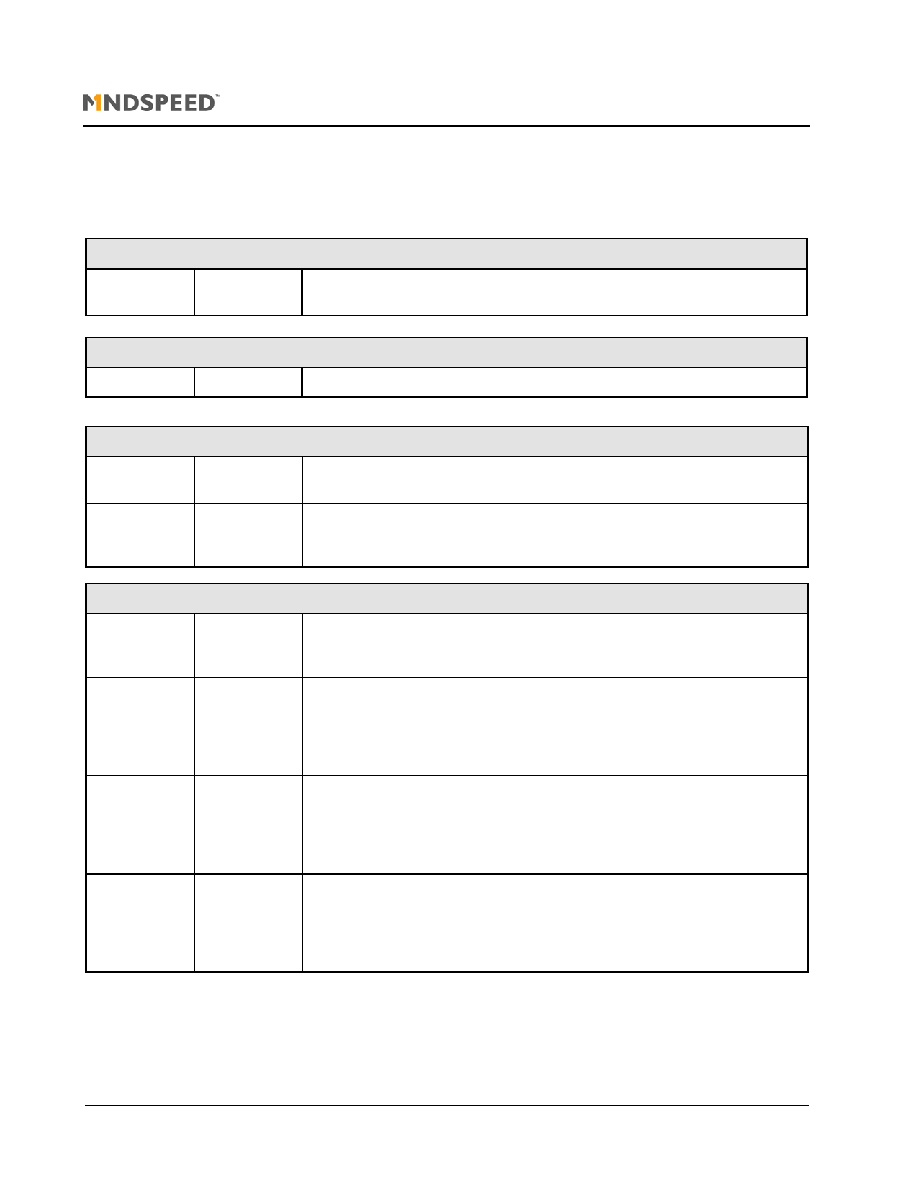
Table 9. Absolute Maximum Ratings
(1)
Symbol
Item
Minimum
Maximum
Units
dv
DD
Digital programming core logic power supply
--
3.6
V
ainv
DD
Switch core/input buffer power supply
--
3.6
V
aoutv
DD
Output drivers power supply
--
3.6
V
T
st
Storage temperature
�65
+150
�C
ESD
Human body model (low-speed)
1500
--
V
ESD
Human body model (high-speed)
800
--
V
ESD
Charge device model
200
--
V
Note:
1. Normal operating conditions for the M21120 are specified in
Table 7
. Extended exposure to Absolute Maximum Ratings in
Table 9
can affect
product reliability.

M21120
34 x 34 3.2 Gbps Crosspoint Switch with Input Equalization
21120-DSH-001-B, 3/27/03
Page 12 of 38
Mindspeed TechnologiesTM
Serial Interface and Switch Programming
Introduction
The crosspoint switch uses +2.5 or 3.3 V CMOS interface levels to program the Switch State (SS). All control inputs have a 50 k
internal pull-up except for xInDis and xOutDis, which have internal pull-downs. The communication protocol may be either a serial
synchronous interface or an 8-bit parallel asynchronous interface. Either interface can:
1. Program the switch state
2. Individually enable/disable inputs/outputs
3. Access control registers and auxiliary functions
4. Read back the current state of the switch
This section details the operation of the I/O interface and switch programming. The auxiliary functions and address mapping are
explained in the section, Switch Function Details.
Register Concept
The various switch functions are controlled by 8-bit registers that are addressed by the 8-bit address (ADDR) bus. The register
contents are transferred via the 8-bit data (DATA) bus during a READ or WRITE.
Switch State Register Concept
The Switch State of the crosspoint switch uses a double buffered register. The Active Configuration Latch (ACL) holds the current
switch setting while the Input Configuration Latch (ICL) holds either the current switch setting or the next switch setting, depending on
the mode of operation.
The xSET Mode register (ADDR=E7h) selects the two modes of operation. DATA=00h enables Mode 1, which is the default mode
after a reset. In Mode 1, the switch state changes with each WRITE to the register that determines the SS. In the WRITE mode, as
xDS goes low, the input channel specified by DATA for the output selected by ADDR passes directly through the double buffer (ICL/
ACL), which routes the selected input to the newly selected output channel. On the rising edge of xDS, ICL and ACL both store (latch)
this SS.
Figure 3
represents a timing diagram for the Parallel I/O, Mode 1.
In Mode 2, the SS is written first to the ICL and the switch state does not change. With either the hardware or software xSET
command, the contents of the ICL transfer to the ACL, changing the SS. This mode allows 1 to 68 channels to change simultaneously.
The hardware xSET mode is enabled by DATA=10b written into xSET Mode (ADDR=E7h). On the falling edge of xSet, the contents of
the ICL pass to the ACL, changing the SS. On the rising edge of xSet, the SS is latched.
Figure 3
illustrates the timing for a parallel
write operation.
Figure 4
illustrates the timing for a parallel read operation.
Table 10
defines the timing specifications for parallel write
operations.
Table 11
defines the timing specifications for parallel read operations.
To enable the software xSet mode, where the xSet command is sent via a software command rather than a hardware command, a
value of 01h should be written into the xSET Mode register (address E7h). Once in the software xSet mode, an xSet command can be
issued with a write of any value to the software xSET register (address E8h). A write of any value to the software xSET register
(address E8h) will update the ACL with the current ICL contents and change the switch state.

M21120
34 x 34 3.2 Gbps Crosspoint Switch with Input Equalization
21120-DSH-001-B, 3/27/03
Page 13 of 38
Mindspeed TechnologiesTM
Figure 3. Parallel Write Timing Diagram
Figure 4. Parallel Read Timing Diagram
xCS
R_xW
xDS
A[9:0]
D[7:0]
Address
Data Write
t
Scs_w
t
Hcs_w
t
Srw_w
t
Hrw_w
t
SA_w
t
HA_w
t
TxDS_lo_w
t
TxDS_hi_w
t
SD
t
HD
Write Access
xSET
t
Sets
t
Setw
Data is latched on rising edge of xDS
xCS
R_xW
xDS
A[9:0]
D[7:0]
Address
Data Read
t
Scs_r
t
Hcs_r
t
Srw_r
t
Hrw_r
t
SA_r
t
HA_r
t
TxDS_lo_r
t
TxDS_hi_r
Read Access
t
A2out
M21120
34 x 34 3.2 Gbps Crosspoint Switch with Input Equalization
21120-DSH-001-B, 3/27/03
Page 14 of 38
Mindspeed TechnologiesTM
Table 10. Parallel Timing Specifications For Write Operations
Parameter
Description
Minimum
Typical
Maximum
tScs_w
xCS Falling Edge before xDS Falling Edge
5 ns
--
--
tHcs_w
xCS Hold after Rising Edge of xDS
0 ns
--
--
tHrw_w
R/xW Hold after Rising Edge of xDS
0 ns
--
--
tSrw_w
R/xW Setup before Falling Edge of xDS
9 ns
--
--
tTxDSl_w
xDS Low Period
5 ns
--
--
tTxDSh_w
xDS High Period
5 ns
--
--
tSA_w
Address Setup before Falling Edge of xDS
4 ns
--
--
tHA_w
Address Hold after Rising Edge of xDS
2 ns
--
--
tSD_w
Data Setup before Falling Edge of xDS
7 ns
--
--
tHD_w
Data Hold after Rising Edge of xDS
2 ns
--
--
tsetw
Hardware xSet pulse width
5 ns
--
--
tsets
Hardware xSet setup time
8 ns
--
--
Table 11. Parallel TIming Specifications For Read Operations
Parameter
Description
Minimum
Typical
Maximum
tScs_r
xCS Falling Edge before xDS Falling Edge
0 ns
--
--
tHcs_r
xCS Hold after Rising Edge of xDS
0 ns
--
--
tHrw_r
R/xW Hold after Rising Edge of xDS
0 ns
--
--
tSrw_r
R/xW Setup before Falling Edge of xDS
12 ns
--
--
tTxDSl_r
xDS Low Period
17 ns
--
--
tTxDSh_r
xDS High Period
17 ns
--
--
tSA_r
Address Setup before Falling Edge of xDS
6 ns
--
--
tHA_r
Address Hold after Rising Edge of xDS
2 ns
--
--
ta2out
Address Valid to Data Valid (on Read)
--
--
12 ns
M21120
34 x 34 3.2 Gbps Crosspoint Switch with Input Equalization
21120-DSH-001-B, 3/27/03
Page 15 of 38
Mindspeed TechnologiesTM
Parallel I/O Overview
Setting the hardware pin Ser/xPar low enables the parallel I/O mode. An 8-bit address bus addresses the register and a bi-directional
8-bit data bus can read and write the register contents. The active low data strobe (xDS) latches (stores) the data in the register on
the rising edge of xDS. The double buffer (ICL/ACL) is transparent to the data (mode 1) when xDS=L, so the SS will change on the
falling edge of xDS. On the rising edge of xDS, the switch state will be stored into the register. The active low pin xCS gates the I/O
and the R/xW gates whether a read or write operation is being performed. During a read operation, the current configuration of the
addressed channel is read back from the device if a read is to an output channel register, regardless of the contents of the ICL.
Serial I/O Overview
To configure the M21120 for the serial programming mode, the hardware pin Ser/xPar must be high. A serial I/O operation is initiated
when xCS transitions from a high state to a low state. Data is shifted in on SDI on the falling edge of SCLK, and shifted out on SDO
on the rising edge of SCLK. A 10-bit sequence addresses a register, as illustrated in
Figure 5
. The Start Bit (SB) is first in the bit
sequence, followed by the Operation Bit (OP) and the 8-bit ADDR (MSB first). For a write operation, an 8-bit DATA (MSB first) directly
follows the last address bit. The start bit is 1 in all cases, and the operation bit is 1 for a read and 0 for a write operation.
Figure 5. Serial Word Format
Figure 6
illustrates the serial Write mode timing diagram. To initiate a Write sequence, xCS goes low before the falling edge of SCLK.
On each falling edge of SCLK, the 18-bits consisting of the SB = 1, OP = 0, ADDR, and DATA, are latched into the input shift register.
The rising edge of xCS must occur before the falling edge of SCLK for the last bit. Upon receipt of the last bit, one additional cycle of
SCLK is necessary before the input DATA transfers from the input shift register to the addressed register. If consecutive read/write
cycles are being performed, it is not necessary to insert an extra clock cycle between read/write cycles, however one extra clock cycle
is needed after the last data bit of the final read/write cycle to complete the operation.
Figure 6. Serial Write Mode
1
rw
A[7:0]
D[7:0]
17 16
15
8
7
0
Start Bit
Read/Write
Address
Data
LSB
MSB
MSB
LSB
a7
a6
a5
a4
a3
a2
a1
a0
d7
d6
d5
d4
d3
d2
d1
d0
1
wr
1
Tdw
Tdh
Tds
Tens
Tclk
Twclk
SCLK
xCS
SDI
Tcs
Tch
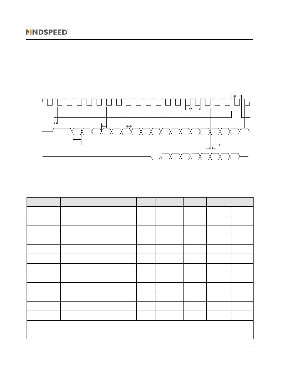
M21120
34 x 34 3.2 Gbps Crosspoint Switch with Input Equalization
21120-DSH-001-B, 3/27/03
Page 16 of 38
Mindspeed TechnologiesTM
Figure 7
illustrates the serial Read mode timing diagram. To initiate a read sequence, xCS goes low before the falling edge of SCLK.
On each falling edge of SCLK, the 10-bits consisting of SB = 1, OP = 1, and the 8-bit ADDR are written to the serial input shift register
of the M21120. On the first rising edge following the address LSB, the SB and 8-bits of the DATA are shifted out on SDO. The first bit
output on SDO for a read operation is always 0.
Figure 7. Serial Read Mode
On a Write cycle, any bits that follow the expected number of bits are ignored, and only the first 16-bits following SB and OP are used.
On a Read cycle, any extra clock cycles will result in the repeat of the data LSB. An invalid SB or OP renders the operation undefined.
The falling edge of xCS always resets the serial operation for a new Read or Write cycle.
Table 12
contains the timing specifications
for the serial programming interface.
Table 12. Serial Interface Timing � Specified at Recommended Operating Conditions
Symbol
Item
Notes
Minimum
Typical
Maximum
Units
t
dw
Data width
--
20
--
--
ns
t
dh
Data hold time
--
5
--
--
ns
t
ds
Data setup time
--
5
--
--
ns
t
ens
Enable setup time
--
5
--
--
ns
t
cs
Chip select setup time
--
2
--
Tclk - 2
ns
t
ch
Chip select hold time
--
2
--
--
ns
t
rdd
Read data output delay
--
1
--
15
ns
t
rds
Read data valid
--
Tclk-15
--
--
ns
t
clk
SCLK period width
--
20
--
--
ns
t
wclk
SCLK minimum low duration
--
5
--
Tclk - 5
ns
t
r
Output rise time
1
--
--
4
ns
t
f
Output fall time
1
--
--
4
ns
Notes:
1. Edge rate in the high edge-rate mode.
a7
a6
a5
a4
a3
a2
a1
a0
X
X
X
X
X
X
X
X
1
rd
1
d7
d6
d5
d4
d3
d2
d1
d0
0
X
SCLK
xCS
SDI
SDO
Trdd
Trds
Tdw
Tens
Tds
Tdh
Twclk
Tclk
Tcs
Tch

M21120
34 x 34 3.2 Gbps Crosspoint Switch with Input Equalization
21120-DSH-001-B, 3/27/03
Page 17 of 38
Mindspeed TechnologiesTM
Switch Function Details
Introduction
The many functions and options of the crosspoint can be accessed through hardware pins or by software via the serial/parallel
interface. In some cases, both software and hardware can access the same function. This section describes the various functions in
detail, which are listed in
Table 8
and
Table 9
.
Input Equalization
To reduce jitter caused by inter-symbol-interference (ISI), input equalization (IE) circuitry is integrated into each input channel of the
M21120. ISI is typically generated when the signal is routed through long PCB traces, cables, or backplane connectors. The IE circuit
for each input channel is enabled by default. The IE for each channel can be individually enabled/disabled through the "I/O Individual
Channel Enable" registers, odd numbered addresses 81�C3h. Bit 3 of this register is used to enable or disable the IE. See
Table 13
for details on the register mapping to specific I/O's for these registers. Note that bit 2 of register EBh must be set to "1." Refer to
"Ini-
tialization Sequence" on page 18
.
Switch Setting
The previous section described the details of the programming interface for register writing, reading, and configuring the switch.
Table 16
lists the allowable addresses for the crosspoint switch. The input channel selection registers are mapped to
ADDR=00h...21h. ADDR 00h is assigned to output channel 0, ADDR 01h to output channel 1, and ADDR 21h to output channel 33.
DATA associated with ADDR are odd numbers from 01h to 43h and are mapped to the input channel that is routed to the selected
output. For example, if ADDR=05h and DATA=01h, then output #5 gets input #0. Refer to
Table 15
for the channel number offset
information. To Read the current configuration of a particular output channel, the selected channel is specified by ADDR and the
resulting DATA is the input channel # routed to the selected output. The Next Switch State (NSS) in the ICL cannot be read back if it
differs from the ACL. The default state after power on is undefined for the M21120. Note that bit D[7] of the register data (regardless of
the serial or parallel interface option) is undefined for a READ and ignored for a WRITE.
Input/Output Enable
The xInDis and xOutDis pins will disable the inputs and outputs, respectively. Setting xInDis=L globally disables all inputs and,
conversely, setting xOutDis=L globally disables all outputs. Hardware disable has priority. If not hardware disabled, the inputs and
outputs can be individually enabled/disabled using the I/O individual channel enable registers (ADDR=81h...C3h).
Table 13
shows
the I/O control mapping for these registers. For the outputs, a disabled state implies turning off the output stage current source to save
power. With built-in pull-up resistors, both positive and negative outputs will default to the high logic state when disabled.
xRST/xTEST
The reset function provides a power-on reset and a general reset to default settings for all registers. The xTest pin is used by
Mindspeed Technologies for internal testing and should be tied to V
DD
for normal operation. A hardware reset should be issued to the
M21120 after initial power up. To issue a hardware reset to the M21120, the xRST pin should be pulled low for a minimum of 20 ns and
then pulled to a high state. This will reset all registers to their default settings. Both the ICL and ACL are cleared resulting in the switch
core set to broadcast channel 0 to all channels. PRBS Tx and Rx are disabled and error flags are cleared. After a hardware or
software reset has been issued to the M21120, the recommened initialization sequence should be executed.
If xTest=L after reset, the switch core is in an undefined state and all inputs/outputs are enabled regardless of the I/O enable and I/O
individual channel enable registers' contents. These features are used for Mindspeed Technologies internal die testing. For normal
operation, xTest=H and xRst =H. Issuing a software reset requires two consecutive Writes to the software reset register (ADDR=EFh)
with DATA=01h. If the next Write is not to the software reset register, the register will clear and two additional consecutive Writes will
be needed. A third write to the software reset register is required to bring the device out of reset and restore all register settings to
their default values. A Hardware reset has priority over a software reset.

M21120
34 x 34 3.2 Gbps Crosspoint Switch with Input Equalization
21120-DSH-001-B, 3/27/03
Page 18 of 38
Mindspeed TechnologiesTM
Initialization Sequence
The M21120 requires a hardware reset after the initial power up. Following either a software or a hardware reset, the following
sequence should be executed in order to correctly initialize the M21120 for operation.
1. Set bit 2 of register EB to "1"
2. Write data = 44h to registers 22h-43h
Table 13. Bit Function for Individual Channel Enable Registers
(1)
(Sheet 1 of 2)
Register Address
(hex)
Input Channel
Controlled
Output Channel
Controlled
Bit 3: Bypass
input IE
Bit 1: Enable/
Disable Input
Bit 0: Enable/Dis-
able Output
80
--
0
0
0
en_out
81
0
1
byp_eq
en_in
en_out
82
--
2
0
0
en_out
83
1
3
byp_eq
en_in
en_out
84
--
4
0
0
en_out
85
2
5
byp_eq
en_in
en_out
86
--
6
0
0
en_out
87
3
7
byp_eq
en_in
en_out
88
--
8
0
0
en_out
89
4
9
byp_eq
en_in
en_out
8A
--
10
0
0
en_out
8B
5
11
byp_eq
en_in
en_out
8C
--
12
0
0
en_out
8D
6
13
byp_eq
en_in
en_out
8E
--
14
0
0
en_out
8F
7
15
byp_eq
en_in
en_out
90
--
16
0
0
en_out
91
8
17
byp_eq
en_in
en_out
92
--
18
0
0
en_out
93
9
19
byp_eq
en_in
en_out
94
--
20
0
0
en_out
95
10
21
byp_eq
en_in
en_out
96
--
22
0
0
en_out
97
11
23
byp_eq
en_in
en_out
98
--
24
0
0
en_out

M21120
34 x 34 3.2 Gbps Crosspoint Switch with Input Equalization
21120-DSH-001-B, 3/27/03
Page 19 of 38
Mindspeed TechnologiesTM
99
12
25
byp_eq
en_in
en_out
9A
--
26
0
0
en_out
9B
13
27
byp_eq
en_in
en_out
9C
--
28
0
0
en_out
9D
14
29
byp_eq
en_in
en_out
9E
--
30
0
0
en_out
9F
15
31
byp_eq
en_in
en_out
A0
--
32
0
0
en_out
A1
16
33
byp_eq
en_in
en_out
A3
17
byp_eq
en_in
0
A5
18
byp_eq
en_in
0
A7
19
byp_eq
en_in
0
A9
20
byp_eq
en_in
0
AB
21
byp_eq
en_in
0
AD
22
byp_eq
en_in
0
AF
23
byp_eq
en_in
0
B1
24
byp_eq
en_in
0
B3
25
byp_eq
en_in
0
B5
26
byp_eq
en_in
0
B7
27
byp_eq
en_in
0
B9
28
byp_eq
en_in
0
BB
29
byp_eq
en_in
0
BD
30
byp_eq
en_in
0
BF
31
byp_eq
en_in
0
C1
32
byp_eq
en_in
0
C3
33
byp_eq
en_in
0
Note:
1. Bits 7, 6, 5, 4 and 2 in registers 80�C3h are not used and shoult be set to 0.
Table 13. Bit Function for Individual Channel Enable Registers
(1)
(Sheet 2 of 2)
Register Address
(hex)
Input Channel
Controlled
Output Channel
Controlled
Bit 3: Bypass
input IE
Bit 1: Enable/
Disable Input
Bit 0: Enable/Dis-
able Output
M21120
34 x 34 3.2 Gbps Crosspoint Switch with Input Equalization
21120-DSH-001-B, 3/27/03
Page 20 of 38
Mindspeed TechnologiesTM
Revision Code
A read from register ADDR=F0h (chip revision) results in a readback of the official chip version.
PRBS TX and RX
The PRBS TX section provides a NRZ PRBS pattern or a 22-bit programmable pattern. The data rate of the PRBS Tx output is
determined by the external clock, ClkTxP/ClkTxN (PCML), which is gated by setting the hardware pin external pin xEnTx=L or by
setting the pwr_tx bit of the PRBS power/enable (ADDR=E0h) register. With xEntx=L, output data updates with each rising edge of
ClkTxP. Note that a value of 01h needs to be written into register address E4h to establish the correct seed for the PRBS patterns.
The single-ended output Trig (ClkTxP/16) can be used as a scope trigger to observe the PRBS patterns. The Trig is a PCML output
with a minimum swing of 150 mV. The Trig pin is designed to drive 50
; however, the backmatch is 200 . Data output is via the
differential DoTxP/DoTxN (PCML) pins. The PRBS Rx section takes in a NRZ PRBS pattern and checks for any bit errors. The user
must provide a phase aligned differential clock and data signal for the PRBS receiver, which can be obtained by passing the data
through a clock and data recovery device and connecting the CDR clock and data outputs to the M21120 PRBS Rx inputs. ClkRxP/
ClkRxN clock and DiRxP/DiRxN data are both gated by the external pin xEnRx or the pwr_rx bit of the PRBS power/enable
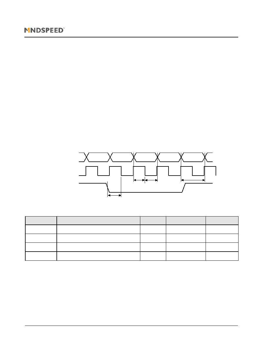
(ADDR=E0h) register. The falling edge of ClkRxP is expected near the middle of the data eye as illustrated in
Figure 8
. The PRBS
Receiver Program timing parameters are listed in
Table 14
.
Figure 8. PRBS Receiver Timing
When the PRBS RX detects an error, PError will be high. The first and each subsequent error will increment an internal
8-bit counter (PRBS RX error count register ADDR=E2h). If the errors exceed 256 (counter overflow), the counter will stay at 255 until
a hardware or software reset. To read the RX error counter register requires a WRITE of any value to copy the current contents of the
running error register into the PRBS RX error count register. A subsequent READ yields the error count as of the last WRITE. The RX
reset can be initiated by the xRstRx pin or by the rst_rx bit in the PRBS control (ADDR=E1h) register. Upon reset, the PRBS RX error
counter clears and PError resets.
PRBS RX error count will always contain the current value of the error count register. Dividing the value by the time of the test is a
rough estimate of the bit error rate. If there has been more that 256 errors, the PRBS RX error count register will always read FFh until
cleared.
Table 14. PRBS Receiver Timing
Parameter
Description
Min
Typical
Max
t
en,
RX
Rx En setup time before falling edge of CLKRx
15 ns
--
--
t
s,
RX
Rx setup time before falling edge of CLKRx
15 ps
�30 ps
--
T
h,
RX
Rx hold time after falling edge of CLKRx
95 ps
50 ps
--
T
w,
RX
Pulse width of CLKRx
310 ps
402 ps
--
A
B
C
D
E
CLKRXP/N
DIRXP/N
xENRX
t
s,RX
t
h,RX
t
en,RX
t
w,RX

M21120
34 x 34 3.2 Gbps Crosspoint Switch with Input Equalization
21120-DSH-001-B, 3/27/03
Page 21 of 38
Mindspeed TechnologiesTM
The PRBS pattern length register (ADDR=E3h) sets the pattern length (n) of a 2
n
-1 pattern. D1 and D0 (rxlen) set the length of the
PRBS Rx and D2 is the rxcirc bit. If D2=L, then the first `n' bits check the input pattern. If the first 23-bits are error free, then each
additional error is counted once. If D2=H, the recirculation mode is enabled and the last `n' bits check the n+1 bit. If a bit error did
occur, the error bit would shift through the `n' bits of the reference resulting in multiple error counts due to one error. Bits D3 and D4
(txlen) determine the pattern length of the PRBS TX. For both the rxlen and txlen:
Value 00b produces a 2
7
-1 pattern with the polynomial D7+D6+1.
Value 01b produces a 2
15
-1 pattern with the polynomial D15+D14+1
Value 10b produces a 2
23
-1 pattern with the polynomial D23+D18+1
Value 11b produces a repeating 22-bit pattern.
For the 2
n
-1, the higher bit patterns conform to the specification, Consultative Committee on Industrial Telegraph and Telephony
(CCITT) Rec. 0.151. The lower pattern is commonly used with commercially available bit error rate testers. The 22-bit pattern is a
repeating user-programmed pattern. The error counter will work with all four patterns.
The TX starting pattern used for all four pattern modes can be user programmed with the three PRBS pattern registers, ADDR=E4
through E6h. ADDR=E4h specifies the first 8-bits (Pattern[0 .. 7] of the user pattern, ADDR=E5h specifies the next 8 bits (Pattern[8 ..
15]), and ADDR=E6h specifies the highest seven bits (Pattern[16 .. 22]). An rst_tx and rst_rx (software) needs to be invoked for both
the RX and TX.
To save power, both the PRBS Tx and Rx can be powered off. The PRBS Power/Enable register, ADDR=E0h, controls these
functions.
Core Power Saving
The CoreCtrl register enables the core power-saving modes. Register CoreCtrl[1] = 0 powers down the switch core and the PRBS Tx/
Rx (default power on).
Register CoreCtrl[0] = 1 enables the SmartPower
core control (default).
Smartpower reduces power dissipation by as much as 30% by automatically powering down unused circuitry in the switch core once
a switch configuration has been programmed. When the switch configuration is changed, Smartpower will enable/diable the
necessary mux circuitry within the switch core. The actual power savings will vary across different switch configurations. This process
takes approximately 10 ns to complete and will increase the time required to reconfigure the switch core. In applications where the
switch core will be left in the same state for a relatively long period of time this is typically not an issue and is worth the power savings.
In applications where the minimum switch reconfiguration time is needed, such as packet switching applications, Smartpower can be
disabled through software.
Digital Slope Control
High speed interface operation requires high speed rise and fall times throughout the IC and it is possible to generate jitter with the
digital control. To minimize this effect, realizing that not all applications will require the fastest programming times, register SlewCtrPd
sets the drive strength of the data output drivers.
Registers
The data used to program registers 00h through 21h in
Table 16
and
Table 17
are offset with respect to the actual channel number as
shown in
Table 15
:

M21120
34 x 34 3.2 Gbps Crosspoint Switch with Input Equalization
21120-DSH-001-B, 3/27/03
Page 22 of 38
Mindspeed TechnologiesTM
Table 15. Input Channel Number Offsets for Programming Input Channel Selection Registers (00�21h)
M21120 Input
Channel No.
Programming Data Value
(Decimal)
Programming Data Value
(Hex)
0
1
01
1
3
03
2
5
05
3
7
07
4
9
09
5
11
0B
6
13
0D
7
15
0F
8
17
11
9
19
13
10
21
15
11
23
17
12
25
19
13
27
1B
14
29
1D
15
31
1F
16
33
21
17
35
23
18
37
25
19
39
27
20
41
29
21
43
2B
22
45
2D
23
47
2F
24
49
31
25
51
33
26
53
35
27
55
37
28
57
39
29
59
3B
30
61
3D
31
63
3F
32
65
41
33
67
43
M21120
34 x 34 3.2 Gbps Crosspoint Switch with Input Equalization
21120-DSH-001-B, 3/27/03
Page 23 of 38
Mindspeed TechnologiesTM
Table 16. Register Summary (Sheet 1 of 2)
(1)
(2)
Address
Register Name
d7
d6
d5
d4
d3
d2
d1
d0
00
R/W In#Data to Out#0
(Note 3)
D[6]
D[5]
D[5]
D[3]
D[2]
D[1]
D[0]
01
R/W In#Data to Out#1
(Note 3)
D[6]
D[5]
D[5]
D[3]
D[2]
D[1]
D[0]
02
R/W In#Data to Out#2
(Note 3)
D[6]
D[5]
D[5]
D[3]
D[2]
D[1]
D[0]
21
R/W In#Data to Out#33
(Note 3)
D[6]
D[5]
D[5]
D[3]
D[2]
D[1]
D[0]
80
Enable Out Channel #0
(Note 4)
ioen[0]
81
Enable In Ch. #0/Out Ch.
#1 (Note 4)
ioen[2]
ioen[1]
ioen[0]
82
Enable Out Channel #2
(Note 4)
ioen[0]
9F
Enable In Ch. #15/Out
Ch. #31 (Note 4)
ioen[2]
ioen[1]
ioen[0]
A0
Enable Out Channel #32
(Note 4)
ioen[0]
A1
Enable In Ch#16/Out Ch.
#33 (Note 4)
ioen[2]
ioen[1]
ioen[0]
A3
Enable In Channel #17
(Note 4)
ioen[2]
ioen[1]
C1
Enable in Channel #32
(Note 4)
ioen[2]
ioen[1]
C3
Enable In Channel #33
(Note 4)
ioen[2]
ioen[1]
E0
prbs power
pwr_trig
pwr_tx
pwr_rx
en_tx
en_rx
E1
prbs control
rst_tx
rst_rx
E2
prbs RX error count
rxerr[7]
rxerr[6]
rxerr[5]
rxerr[4]
rxerr[3]
rxerr[2]
rxerr[1]
rxerr[0]
E3
prbs pattern length
txlen[1]
txlen[0]
rxcirc
rxlen[1]
rxlen[0]
E4
prbs pattern [7:0]
pat[7]
pat[6]
pat[5]
pat[4]
pat[3]
pat[2]
pat[1]
pat[0]

M21120
34 x 34 3.2 Gbps Crosspoint Switch with Input Equalization
21120-DSH-001-B, 3/27/03
Page 24 of 38
Mindspeed TechnologiesTM
E5
prbs pattern [15:8]
pat[15]
pat[14]
pat[13]
pat[12]
pat[11]
pat[10]
pat[9]
pat[8]
E6
prbs pattern [22:16]
pat[22]
pat[21]
pat[20]
pat[19]
pat[18]
pat[17]
pat[16]
E7
xSET mode
xset[1]
xset[0]
E8
software xSET
EB
Mindspeed reserved
1 (Note 5)
EC
core control
en_refs
en_lp
ED
slope control internal
muxdrv
coredrv[1]
coredrv[0]
ifdrv[1]
Ifdrv[0]
clkdrv[1]
clkdrv[0]
EE
slope control pad
paddrv[1]
paddrv[0]
EF
software reset
srst[0]
F0
chip revision
rev[7]
rev[6]
rev[5]
rev[5]
rev[3]
rev[2]
rev[1]
rev[0]
Notes:
1. D[7] ... D[0] represent the internal bus which is mapped to the registers in both the serial and parallel mode.
2. Blank registers bits are undefined and should be set to 0 unless otherwise noted.
3. See
Table 15
for programming values.
4. See
Table 13
for programming details.
5. This bit must be set to 1. Refer to
"Initialization Sequence" on page 18
.
Table 16. Register Summary (Sheet 2 of 2)
(1)
(2)
Address
Register Name
d7
d6
d5
d4
d3
d2
d1
d0
M21120
34 x 34 3.2 Gbps Crosspoint Switch with Input Equalization
21120-DSH-001-B, 3/27/03
Page 25 of 38
Mindspeed TechnologiesTM
Table 17. Register Description
00-21h: Input Channel Selection
D[7:0]
inchannel
Select input channel to route to addressed output
In#0 = 01h, In#1 = 03h,...In#33 = 43h (See
Table 15
.)
Default D[7:0] = 00h
80-C3h: I/O Individual Channel Enable (See
Table 13
)
ioen[2]
byp_eq
0: Input equalization is enabled (default)
1: Input equalization is bypassed
ioen[1]
en_in
0: Input off (default)
1: Input on
ioen[0]
en_out
0: Output off (default)
1: Output on
E0h: PRBS Power
4
pwr_trig
0: TX PRBS trigger power down (default)
1: TX PRBS trigger powered up
3
pwr_tx
0: TX PRBS power down (default)
1: TX PRBS powered up
2
pwr_rx
0: RX PRBS power down (default)
1: RX PRBS powered up
1
en_tx
0: TX PRBS disabled (default)
1: TX PRBS enabled
0
en_rx
0: RX PRBS disabled (default)
1: RX PRBS enabled
E1h: PRBS Control
2
rst_tx
0: normal operation (default)
1: reset TX shift register
1
rst_rx
0: normal operation (default)
1: reset RX shift register
E2h: PRBS RX error count
7..0
rxerr[7:0]
PRBS RX error count register (read only)
M21120
34 x 34 3.2 Gbps Crosspoint Switch with Input Equalization
21120-DSH-001-B, 3/27/03
Page 26 of 38
Mindspeed TechnologiesTM
Table 16. Register Description (Continued)
E3h: PRBS Pattern Length
4..3
txlen[1:0]
Selects TX PRBS pattern length.
00: 2
7
-1 (default)
01: 2
15
-1
10: 2
23
-1
11: 22-bit repeating pattern
2
rxcirc
0: recirculation mode disabled (default)
1: recirculation mode enabled
1..0
rxlen[1:0]
Selects RX PRBS pattern length.
00: 2
7
-1 (default)
01: 2
15
-1
10: 2
23
-1
11: 22-bit repeating pattern
E4h: PRBS Pattern [7:0]
7..0
pattern[7:0]
Value is being loaded into PRBS TX shift register when bit rst_tx = 1 (reg e1h, bit-1). Default =
00h. NOTE: Must be set to 01h for PRBS Tx operation.
E5h: PRBS Pattern [15:8]
7..0
pattern[15:8]
Value is being loaded into PRBS TX shift register when bit rst_tx = 1
(reg e1h, bit-1). Default = 00h
E6h: PRBS Pattern [22:16]
6..0
pattern[22:16]
Value is being loaded into PRBS TX shift register when bit rst_tx = 1
(reg e1h, bit-1). Default = 00h
E7h: xSET Mode
1..0
xset[1:0]
Selects the xSET mode.
00: ACL latches are transparent. Any switch setting written immediately affects the core
configuration. (default)
01: ACL latches are controlled through register e8h (software xSET).
10: ACL latches are controlled by pin xSET (hardware control).
M21120
34 x 34 3.2 Gbps Crosspoint Switch with Input Equalization
21120-DSH-001-B, 3/27/03
Page 27 of 38
Mindspeed TechnologiesTM
Table 16. Register Description (Continued)
E8h: software xSET
Register e7h (xSET mode) needs to be set to 1 in order for this register to have any function.
Any value written to this register will update the ACL with the data from the ICL.
EBh: Mindspeed reserved
2
This bit must be set to 1.
ECh: core control
1
en_refs
0: all references down
1: references powered up (default)
0
en_lp
Core SmartPowerTM control.
0: core fully powered
1: core in low power mode (default)
EDh: slope control internal
6
muxdrv
MUX SELECT LINE slopes.
0: High drive (default)
1: Low drive.
5:4
coredrv[1:0]
READ BACK SPEED (Read back slope control)
00: high drive (default)
01: medium drive
10: low drive
11: tiny drive
3:2
ifdrv[1:0]
WRITE SPEED (Write slope control)
00: high drive (default)
01: medium drive
10: low drive
11: tiny drive
1:0
clkdrv[1:0]
CLOCK distribution slope
00: high drive (default)
01: medium drive
10: low drive
11: tiny drive
M21120
34 x 34 3.2 Gbps Crosspoint Switch with Input Equalization
21120-DSH-001-B, 3/27/03
Page 28 of 38
Mindspeed TechnologiesTM
Table 16. Register Description (Continued)
EEh: slope control pad
1..0
paddrv[1:0]
PAD DRIVE.
00: high drive (default)
01: medium drive
10: low drive
11: three-state
EFh: software reset
1
srst0
Software reset: Needs two consecutive Writes with DATA = 01h.
If second Write is not a reset, register is cleared.
Default (DATA = 00h) third Write required to bring out of reset.
F0h: Chip revision
7:0
Rev [7:0]
Contains the chip revision ( read only )
M21120
34 x 34 3.2 Gbps Crosspoint Switch with Input Equalization
21120-DSH-001-B, 3/27/03
Page 29 of 38
Mindspeed TechnologiesTM
Package Information
Figure 9
gives the overall package dimensions,
Figure 10
shows the package cross section, and
Figure 11
is the bottom view of the
M21120 package showing the ball assignments. All dimensions in the following illustrations are in millimeters.
Figure 9. Package Dimensions
Figure 10. Package Cross Section
Top View
Side View
Seating Plane
0.5mm
2.14mm
35mm
35mm
A1 Ball
Location
>0.5
0.60 Minimum
Optional Edge (Routed)
M21120
34 x 34 3.2 Gbps Crosspoint Switch with Input Equalization
21120-DSH-001-B, 3/27/03
Page 30 of 38
Mindspeed TechnologiesTM
Figure 11. Package Bottom View with Ball Assignments
A1 Ball
Location
A
C
B
D
E
F
G
H
J
K
L
M
N
P
R
T
U
V
W
Y
AA
AB
AC
AD
AE
AF
AG
AH
AJ
AK
AL
AM
AN
AP
1
2
3
4
5
6
7
8
9
10
11
12
13
14
15
16
17
18
19
20
21
22
23
24
25
26
27
28
29
30
31
32
33
34
1mm
33mm
33mm
0.65mm

M21120
34 x 34 3.2 Gbps Crosspoint Switch with Input Equalization
21120-DSH-001-B, 3/27/03
Page 31 of 38
Mindspeed TechnologiesTM
Table 18. Ball List Sorted by Ball Location (Sheet 1 of 3)
Name
Ball
Name
Ball
Name
Ball
Name
Ball
Name
Ball
Name
Ball
Name
Ball
dvss
A1
outp2
B6
outn12
C11
avss
D16
nc
E21
nc
H30
nc
M5
dvss
A2
outn2
B7
aoutvdd
C12
outp30
D17
nc
E22
nc
H31
nc
M30
dvdd
A3
avss
B8
outp20
C13
outn30
D18
nc
E23
nc
H32
nc
M31
nc
A4
outp10
B9
outn20
C14
avss
D19
nc
E24
avss
H33
ainvdd
M32
aoutvdd
A5
outn10
B10
aoutvdd
C15
nc
D20
nc
E25
ainvdd
H34
nc
M33
outp0
A6
avss
B11
outp28
C16
nc
D21
nc
E26
inn5
J1
nc
M34
outn0
A7
outp18
B12
outn28
C17
avss
D22
nc
E27
inn4
J2
ainvdd
N1
aoutvdd
A8
outn18
B13
aoutvdd
C18
nc
D23
nc
E28
ainvdd
J3
avss
N2
outp8
A9
avss
B14
nc
C19
nc
D24
nc
E29
inp6
J4
inp11
N3
outn8
A10
outp26
B15
nc
C20
avss
D25
nc
E30
d[2]
J5
inn10
N4
aoutvdd
A11
outn26
B16
aoutvdd
C21
nc
D26
xenrx
E31
nc
J30
nc
N5
outp16
A12
avss
B17
nc
C22
nc
D27
nc
E32
nc
J31
nc
N30
outn16
A13
nc
B18
nc
C23
avss
D28
avss
E33
ainvdd
J32
avss
N31
aoutvdd
A14
nc
B19
aoutvdd
C24
nc
D29
ainvdd
E34
nc
J33
nc
N32
outp24
A15
avss
B20
nc
C25
nc
D30
inn1
F1
nc
J34
nc
N33
outn24
A16
nc
B21
nc
C26
dirxn
D31
inn0
F2
ainvdd
K1
nc
N34
aoutvdd
A17
nc
B22
aoutvdd
C27
xoutdis
D32
d[1]
F3
avss
K2
inp13
P1
outp32
A18
avss
B23
nc
C28
perror
D33
inp2
F4
inp7
K3
inp12
P2
outn32
A19
nc
B24
nc
C29
nc
D34
d[5]
F5
inn6
K4
inn11
P3
aoutvdd
A20
nc
B25
xtest
C30
inp1
E1
nc
F30
d[0]
K5
avss
P4
nc
A21
avss
B26
clkrxn
C31
inp0
E2
xrstrx
F31
nc
K30
nc
P5
nc
A22
nc
B27
xrst
C32
xcs
E3
ainvdd
F32
avss
K31
nc
P30
aoutvdd
A23
nc
B28
dirxp
C33
a[0]
E4
nc
F33
nc
K32
nc
P31
nc
A24
avss
B29
nc
C34
a[1]
E5
nc
F34
nc
K33
nc
P32
nc
A25
nc
B30
ainvdd
D1
a[3]
E6
ainvdd
G1
nc
K34
avss
P33
aoutvdd
A26
nc
B31
d[3]
D2
a[6]
E7
avss
G2
inp9
L1
ainvdd
P34
nc
A27
clkrxp
B32
d[7]/do
D3
a[5]
E8
inp3
G3
inp8
L2
inn13
R1
nc
A28
nc
B33
xds/sclk
D4
nc
E9
inn2
G4
inn7
L3
inn12
R2
aoutvdd
A29
nc
B34
a[7]
D5
nc
E10
d[6]/di
G5
avss
L4
ainvdd
R3
nc
A30
dvdd
C1
xset
D6
nc
E11
nc
G30
nc
L5
inp14
R4
nc
A31
dvdd
C2
avss
D7
nc
E12
avss
G31
nc
L30
nc
R5
aoutvdd
A32
a[2]
C3
outp6
D8
nc
E13
nc
G32
nc
L31
nc
R30
nc
A33
a[4]
C4
outn6
D9
nc
E14
nc
G33
nc
L32
nc
R31
nc
A34
r/xw
C5
avss
D10
nc
E15
nc
G34
avss
L33
ainvdd
R32
dvss
B1
aoutvdd
C6
outp14
D11
nc
E16
inp5
H1
ainvdd
L34
nc
R33
dvss
B2
outp4
C7
outn14
D12
nc
E17
inp4
H2
inn9
M1
nc
R34
dvdd
B3
outn4
C8
avss
D13
nc
E18
inn3
H3
inn8
M2
ainvdd
T1
nc
B4
aoutvdd
C9
outp22
D14
nc
E19
avss
H4
ainvdd
M3
avss
T2
avss
B5
outp12
C10
outn22
D15
nc
E20
d[4]
H5
inp10
M4
inp15
T3

M21120
34 x 34 3.2 Gbps Crosspoint Switch with Input Equalization
21120-DSH-001-B, 3/27/03
Page 32 of 38
Mindspeed TechnologiesTM
inn14
T4
avss
Y4
inp26
AD4
inn30
AH4
nc
AK24
trig
AL30
xindis
AN2
nc
T5
nc
Y5
nc
AD5
nc
AH5
nc
AK25
nc
AL31
avss
AN3
nc
T30
nc
Y30
nc
AD30
nc
AH30
nc
AK26
nc
AL32
avss
AN4
avss
T31
nc
Y31
nc
AD31
avss
AH31
nc
AK27
nc
AL33
outp1
AN5
nc
T32
nc
Y32
ainvdd
AD32
nc
AH32
nc
AK28
nc
AL34
outn1
AN6
nc
T33
avss
Y33
nc
AD33
nc
AH33
nc
AK29
ainvdd
AM1
avss
AN7
nc
T34
ainvdd
Y34
nc
AD34
nc
AH34
nc
AK30
avss
AM2
outp9
AN8
inp17
U1
inn21
AA1
ainvdd
AE1
inp33
AJ1
nc
AK31
nc
AM3
outn9
AN9
inp16
U2
inn20
AA2
avss
AE2
inp32
AJ2
dotxp
AK32
cnxt_test
AM4
avss
AN10
inn15
U3
ainvdd
AA3
inp27
AE3
inn31
AJ3
nc
AK33
aoutvdd
AM5
outp17
AN11
avss
U4
inp22
AA4
inn26
AE4
avss
AJ4
nc
AK34
aoutvdd
AM6
outn17
AN12
nc
U5
nc
AA5
nc
AE5
nc
AJ5
ainvdd
AL1
outp7
AM7
avss
AN13
nc
U30
nc
AA30
nc
AE30
nc
AJ30
avss
AL2
outn7
AM8
outp25
AN14
nc
U31
nc
AA31
avss
AE31
nc
AJ31
ainvdd
AL3
aoutvdd
AM9
outn25
AN15
nc
U32
ainvdd
AA32
nc
AE32
nc
AJ32
nc
AL4
outp15
AM10
avss
AN16
avss
U33
nc
AA33
nc
AE33
avss
AJ33
nc
AL5
outn15
AM11
outp33
AN17
ainvdd
U34
nc
AA34
nc
AE34
ainvdd
AJ34
outp5
AL6
aoutvdd
AM12
outn33
AN18
inn17
V1
ainvdd
AB1
inp29
AF1
inn33
AK1
outn5
AL7
outp23
AM13
avss
AN19
inn16
V2
avss
AB2
inp28
AF2
inn32
AK2
avss
AL8
outn23
AM14
nc
AN20
ainvdd
V3
inp23
AB3
inn27
AF3
ainvdd
AK3
outp13
AL9
aoutvdd
AM15
nc
AN21
inp18
V4
inn22
AB4
avss
AF4
nc
AK4
outn13
AL10
outp31
AM16
avss
AN22
nc
V5
nc
AB5
nc
AF5
nc
AK5
avss
AL11
outn31
AM17
nc
AN23
nc
V30
nc
AB30
nc
AF30
nc
AK6
outp21
AL12
aoutvdd
AM18
nc
AN24
nc
V31
avss
AB31
nc
AF31
nc
AK7
outn21
AL13
nc
AM19
avss
AN25
ainvdd
V32
nc
AB32
nc
AF32
nc
AK8
avss
AL14
nc
AM20
nc
AN26
nc
V33
nc
AB33
avss
AF33
nc
AK9
outp29
AL15
aoutvdd
AM21
nc
AN27
nc
V34
nc
AB34
ainvdd
AF34
nc
AK10
outn29
AL16
nc
AM22
avss
AN28
ainvdd
W1
inp25
AC1
inn29
AG1
nc
AK11
avss
AL17
nc
AM23
nc
AN29
avss
W2
inp24
AC2
inn28
AG2
nc
AK12
nc
AL18
aoutvdd
AM24
nc
AN30
inp19
W3
inn23
AC3
ainvdd
AG3
nc
AK13
nc
AL19
nc
AM25
avss
AN31
inn18
W4
avss
AC4
inp30
AG4
nc
AK14
avss
AL20
nc
AM26
clktxn
AN32
nc
W5
nc
AC5
nc
AG5
nc
AK15
nc
AL21
aoutvdd
AM27
nc
AN33
nc
W30
nc
AC30
nc
AG30
nc
AK16
nc
AL22
nc
AM28
xentx
AN34
avss
W31
nc
AC31
nc
AG31
nc
AK17
avss
AL23
nc
AM29
nc
AP1
nc
W32
nc
AC32
ainvdd
AG32
nc
AK18
nc
AL24
aoutvdd
AM30
ser/xpar
AP2
nc
W33
avss
AC33
nc
AG33
nc
AK19
nc
AL25
nc
AM31
nc
AP3
nc
W34
ainvdd
AC34
nc
AG34
nc
AK20
avss
AL26
nc
AM32
aoutvdd
AP4
inp21
Y1
inn25
AD1
ainvdd
AH1
nc
AK21
nc
AL27
dotxn
AM33
outp3
AP5
inp20
Y2
inn24
AD2
avss
AH2
nc
AK22
nc
AL28
ainvdd
AM34
outn3
AP6
inn19
Y3
ainvdd
AD3
inp31
AH3
nc
AK23
avss
AL29
nc
AN1
aoutvdd
AP7
Table 18. Ball List Sorted by Ball Location (Sheet 2 of 3)
Name
Ball
Name
Ball
Name
Ball
Name
Ball
Name
Ball
Name
Ball
Name
Ball

M21120
34 x 34 3.2 Gbps Crosspoint Switch with Input Equalization
21120-DSH-001-B, 3/27/03
Page 33 of 38
Mindspeed TechnologiesTM
outp11
AP8
outn11
AP9
aoutvdd
AP10
outp19
AP11
outn19
AP12
aoutvdd
AP13
outp27
AP14
outn27
AP15
aoutvdd
AP16
nc
AP17
nc
AP18
aoutvdd
AP19
nc
AP20
nc
AP21
aoutvdd
AP22
nc
AP23
nc
AP24
aoutvdd
AP25
nc
AP26
nc
AP27
aoutvdd
AP28
nc
AP29
nc
AP30
aoutvdd
AP31
clktxp
AP32
nc
AP33
nc
AP34
Table 18. Ball List Sorted by Ball Location (Sheet 3 of 3)
Name
Ball
Name
Ball
Name
Ball
Name
Ball
Name
Ball
Name
Ball
Name
Ball

M21120
34 x 34 3.2 Gbps Crosspoint Switch with Input Equalization
21120-DSH-001-B, 3/27/03
Page 34 of 38
Mindspeed TechnologiesTM
Table 19. Ball List Sorted by Ball Name (Sheet 1 of 3)
Name
Ball
Name
Ball
Name
Ball
Name
Ball
Name
Ball
Name
Ball
Name
Ball
a[0]
E4
ainvdd
AH1
aoutvdd AP10
avss
T2
avss
AN31 inn10
N4
inp14
R4
a[1]
E5
ainvdd
AJ34
aoutvdd AP13
avss
T31
avss
Y4
inn11
P3
inp15
T3
a[2]
C3
ainvdd
AK3
aoutvdd AP16
avss
U4
avss
Y33
inn12
R2
inp16
U2
a[3]
E6
ainvdd
AL1
aoutvdd AP19
avss
U33
clkrxn
C31
inn13
R1
inp17
U1
a[4]
C4
ainvdd
AL3
aoutvdd AP22
avss
W2
clkrxp
B32
inn14
T4
inp18
V4
a[5]
E8
ainvdd
AM1
aoutvdd AP25
avss
W31
clktxn
AN32 inn15
U3
inp19
W3
a[6]
E7
ainvdd
AM34 aoutvdd AP28
avss
AB2
clktxp
AP32 inn16
V2
inp20
Y2
a[7]
D5
ainvdd
Y34
aoutvdd AP31
avss
AB31
cnxt_test AM4
inn17
V1
inp21
Y1
ainvdd
D1
aoutvdd
A5
avss
B5
avss
AC4
d[0]
K5
inn18
W4
inp22
AA4
ainvdd
E34
aoutvdd
A8
avss
B8
avss
AC33 d[1]
F3
inn19
Y3
inp23
AB3
ainvdd
F32
aoutvdd
A11
avss
B11
avss
AE2
d[2]
J5
inn20
AA2
inp24
AC2
ainvdd
G1
aoutvdd
A14
avss
B14
avss
AE31
d[3]
D2
inn21
AA1
inp25
AC1
ainvdd
H34
aoutvdd
A17
avss
B17
avss
AF4
d[4]
H5
inn22
AB4
inp26
AD4
ainvdd
J3
aoutvdd
A20
avss
B20
avss
AF33
d[5]
F5
inn23
AC3
inp27
AE3
ainvdd
J32
aoutvdd
A23
avss
B23
avss
AH2
d[6]/di
G5
inn24
AD2
inp28
AF2
ainvdd
K1
aoutvdd
A26
avss
B26
avss
AH31 d[7]/do
D3
inn25
AD1
inp29
AF1
ainvdd
L34
aoutvdd
A29
avss
B29
avss
AJ4
dirxn
D31
inn26
AE4
inp30
AG4
ainvdd
M3
aoutvdd
A32
avss
D7
avss
AJ33
dirxp
C33
inn27
AF3
inp31
AH3
ainvdd
M32
aoutvdd
C6
avss
D10
avss
AL2
dotxn
AM33 inn28
AG2
inp32
AJ2
ainvdd
N1
aoutvdd
C9
avss
D13
avss
AL8
dotxp
AK32 inn29
AG1
inp33
AJ1
ainvdd
P34
aoutvdd
C12
avss
D16
avss
AL11
dvdd
A3
inn30
AH4
nc
A4
ainvdd
R3
aoutvdd
C15
avss
D19
avss
AL14
dvdd
B3
inn31
AJ3
nc
A21
ainvdd
R32
aoutvdd
C18
avss
D22
avss
AL17
dvdd
C1
inn32
AK2
nc
A22
ainvdd
T1
aoutvdd
C21
avss
D25
avss
AL20
dvdd
C2
inn33
AK1
nc
A24
ainvdd
U34
aoutvdd
C24
avss
D28
avss
AL23
dvss
A1
inp0
E2
nc
A25
ainvdd
V3
aoutvdd
C27
avss
E33
avss
AL26
dvss
A2
inp1
E1
nc
A27
ainvdd
V32
aoutvdd
AM5
avss
G2
avss
AL29
dvss
B1
inp2
F4
nc
A28
ainvdd
W1
aoutvdd
AM6
avss
G31
avss
AM2
dvss
B2
inp3
G3
nc
A30
ainvdd
AA3
aoutvdd
AM9
avss
H4
avss
AN3
inn0
F2
inp4
H2
nc
A31
ainvdd
AA32
aoutvdd
AM12 avss
H33
avss
AN4
inn1
F1
inp5
H1
nc
A33
ainvdd
AB1
aoutvdd
AM15 avss
K2
avss
AN7
inn2
G4
inp6
J4
nc
A34
ainvdd
AC34 aoutvdd
AM18 avss
K31
avss
AN10 inn3
H3
inp7
K3
nc
B4
ainvdd
AD3
aoutvdd
AM21 avss
L4
avss
AN13 inn4
J2
inp8
L2
nc
B33
ainvdd
AD32 aoutvdd
AM24 avss
L33
avss
AN16 inn5
J1
inp9
L1
nc
B34
ainvdd
AE1
aoutvdd
AM27 avss
N2
avss
AN19 inn6
K4
inp10
M4
nc
B19
ainvdd
AF34
aoutvdd
AM30 avss
N31
avss
AN22 inn7
L3
inp11
N3
nc
B22
ainvdd
AG3
aoutvdd
AP4
avss
P4
avss
AN25 inn8
M2
inp12
P2
nc
B25
ainvdd
AG32 aoutvdd
AP7
avss
P33
avss
AN28 inn9
M1
inp13
P1
nc
B28

M21120
34 x 34 3.2 Gbps Crosspoint Switch with Input Equalization
21120-DSH-001-B, 3/27/03
Page 35 of 38
Mindspeed TechnologiesTM
nc
B31
nc
E24
nc
N34
nc
AB30
nc
AK7
nc
AL34
outn2
B7
nc
B18
nc
E25
nc
P5
nc
AB32
nc
AK8
nc
AM3
outn3
AP6
nc
B21
nc
E26
nc
P30
nc
AB33
nc
AK9
nc
AM19 outn4
C8
nc
B24
nc
E27
nc
P31
nc
AB34
nc
AK10 nc
AM20 outn5
AL7
nc
B27
nc
E28
nc
P32
nc
AC5
nc
AK11 nc
AM22 outn6
D9
nc
B30
nc
E29
nc
R5
nc
AC30 nc
AK12 nc
AM23 outn7
AM8
nc
C19
nc
E30
nc
R30
nc
AC31 nc
AK13 nc
AM25 outn8
A10
nc
C20
nc
E32
nc
R31
nc
AC32 nc
AK14 nc
AM26 outn9
AN9
nc
C22
nc
F30
nc
R33
nc
AD5
nc
AK15 nc
AM28 outn10
B10
nc
C23
nc
F33
nc
R34
nc
AD30 nc
AK16 nc
AM29 outn11
AP9
nc
C25
nc
F34
nc
T5
nc
AD31 nc
AK17 nc
AM31 outn12
C11
nc
C26
nc
G30
nc
T30
nc
AD33 nc
AK18 nc
AM32 outn13
AL10
nc
C28
nc
G32
nc
T32
nc
AD34 nc
AK19 nc
AN20 outn14
D12
nc
C29
nc
G33
nc
T33
nc
AE5
nc
AK20 nc
AN21 outn15
AM11
nc
C34
nc
G34
nc
T34
nc
AE30
nc
AK21 nc
AN23 outn16
A13
nc
D20
nc
H30
nc
U5
nc
AE32
nc
AK22 nc
AN24 outn17
AN12
nc
D21
nc
H31
nc
U30
nc
AE33
nc
AK23 nc
AN26 outn18
B13
nc
D23
nc
H32
nc
U31
nc
AE34
nc
AK24 nc
AN27 outn19
AP12
nc
D24
nc
J30
nc
U32
nc
AF5
nc
AK25 nc
AN29 outn20
C14
nc
D26
nc
J31
nc
V5
nc
AF30
nc
AK26 nc
AN30 outn21
AL13
nc
D27
nc
J33
nc
V30
nc
AF31
nc
AK27 nc
AN33 outn22
D15
nc
D29
nc
J34
nc
V31
nc
AF32
nc
AK28 nc
AP1
outn23
AM14
nc
D30
nc
K30
nc
V33
nc
AG5
nc
AK29 nc
AP3
outn24
A16
nc
D34
nc
K32
nc
V34
nc
AG30 nc
AK30 nc
AP17 outn25
AN15
nc
E9
nc
K33
nc
W5
nc
AG31 nc
AK31 nc
AP18 outn26
B16
nc
E10
nc
K34
nc
W30
nc
AG33 nc
AK33 nc
AP20 outn27
AP15
nc
E11
nc
L5
nc
W32
nc
AG34 nc
AK34 nc
AP21 outn28
C17
nc
E12
nc
L30
nc
W33
nc
AH5
nc
AL5
nc
AP23 outn29
AL16
nc
E13
nc
L31
nc
W34
nc
AH30 nc
AL18 nc
AP24 outn30
D18
nc
E14
nc
L32
nc
Y5
nc
AH32 nc
AL19 nc
AP26 outn31
AM17
nc
E15
nc
M5
nc
Y30
nc
AH33 nc
AL21 nc
AP27 outn32
A19
nc
E16
nc
M30
nc
Y31
nc
AH34 nc
AL22 nc
AP29 outn33
AN18
nc
E17
nc
M31
nc
Y32
nc
AJ5
nc
AL24 nc
AP30 outp0
A6
nc
E18
nc
M33
nc
AA5
nc
AJ30
nc
AL25 nc
AP33 outp1
AN5
nc
E19
nc
M34
nc
AA30
nc
AJ31
nc
AL27 nc
AP34 outp2
B6
nc
E20
nc
N5
nc
AA31
nc
AJ32
nc
AL28 nc
AL4
outp3
AP5
nc
E21
nc
N30
nc
AA33
nc
AK4
nc
AL31 nc
AN1
outp4
C7
nc
E22
nc
N32
nc
AA34
nc
AK5
nc
AL32 outn0
A7
outp5
AL6
nc
E23
nc
N33
nc
AB5
nc
AK6
nc
AL33 outn1
AN6
outp6
D8
Table 19. Ball List Sorted by Ball Name (Sheet 2 of 3)
Name
Ball
Name
Ball
Name
Ball
Name
Ball
Name
Ball
Name
Ball
Name
Ball

M21120
34 x 34 3.2 Gbps Crosspoint Switch with Input Equalization
21120-DSH-001-B, 3/27/03
Page 36 of 38
Mindspeed TechnologiesTM
outp7
AM7
ser/xpar
AP2
outp8
A9
trig
AL30
outp9
AN8
xcs
E3
outp10
B9
xds/sclk
D4
outp11
AP8
xenrx
E31
outp12
C10
xentx
AN34
outp13
AL9
xindis
AN2
outp14
D11
xoutdis
D32
outp15
AM10 xrst
C32
outp16
A12
xrstrx
F31
outp17
AN11
xset
D6
outp18
B12
xtest
C30
outp19
AP11
outp20
C13
outp21
AL12
outp22
D14
outp23
AM13
outp24
A15
outp25
AN14
outp26
B15
outp27
AP14
outp28
C16
outp29
AL15
outp30
D17
outp31
AM16
outp32
A18
outp33
AN17
perror
D33
r/xw
C5
Table 19. Ball List Sorted by Ball Name (Sheet 3 of 3)
Name
Ball
Name
Ball
Name
Ball
Name
Ball
Name
Ball
Name
Ball
Name
Ball
M21120
� 2003 Mindspeed TechnologiesTM, as a wholly owned subsidiary and the Internet infrastructure business of Conexant
Systems, Inc. All Rights are Reserved.
Information in this document is provided in connection with Mindspeed Technologies, Inc. "Mindspeed" products. These
materials are provided by Mindspeed as a service to its customers and may be used for informational purposes only.
Mindspeed assumes no responsibility for errors or omissions in these materials. Mindspeed may make changes to
specifications and product descriptions at any time, without notice. Mindspeed makes no commitment to update the
information contained herein. Mindspeed shall have no responsibility whatsoever for conflicts or incompatibilities arising
from future changes to its specifications and product descriptions.
No license, express or implied, by estoppel or otherwise, to any intellectual property rights is granted by this document.
Except as provided in Mindspeed Terms and Conditions of Sale for such products, Mindspeed assumes no liability
whatsoever.
THESE MATERIALS ARE PROVIDED "AS IS" WITHOUT WARRANTY OF ANY KIND, EITHER EXPRESS OR IMPLIED,
RELATING TO SALE AND/OR USE OF CONEXANT PRODUCTS INCLUDING LIABILITY OR WARRANTIES RELATING
TO FITNESS FOR A PARTICULAR PURPOSE, MERCHANTABILITY, OR INFRINGEMENT OF ANY PATENT,
COPYRIGHT OR OTHER INTELLECTUAL PROPERTY RIGHT. Mindspeed further does not warrant the accuracy or
completeness of the information, text, graphics or other items contained within these materials. Mindspeed shall not be
liable for any special, indirect, incidental, or consequential damages, including without limitation, lost revenues or lost
profits, which may result from the use of these materials.
Mindspeed products are not intended for use in medical, life saving or life sustaining applications. Mindspeed customers
using or selling Mindspeed products for use in such applications do so at their own risk and agree to fully indemnify
Mindspeed for any damages resulting from such improper use or sale.
The following are trademarks of Mindspeed Technologies, Inc. the symbol M1, MindspeedTM, and "Build It FirstTM" Product
names or services listed in this publication are for identification purposes only, and may be trademarks of third parties.
Third-party brands and names are the property of their respective owners.
For additional disclaimer information, please consult Mindspeed Technologies Legal Information posted at:
http://www.mindspeed.com/, which is incorporated by reference.
Reader Response: Mindspeed Technologies, Inc. strives to produce quality documentation and welcomes your feedback.
Please send comments and suggestions to mailto:tech.pubs@mindspeed.com. For technical questions, or to talk to a field
applications engineer contact your local MindspeedTM sales office listed below. For literature send email request to
literature@mindspeed.com.
34 x 34 3.2 Gbps Crosspoint Switch with Input Equalization
21120-DSH-001-B, 3/27/03
Page 37 of 38
Mindspeed TechnologiesTM
Revision History
Name
Date
Package Data
500289A
2/5/02
Initial release.
500289B
2/9/02
Revision B.
21130-DSH-001-B
3/21/03
Changed document number to new numbering system. Revised parallel
timing diagrams and specifications tables and CMOS DC electrical
specifications tables.

World Wide Sales Companies
21120-DSH-001-B, 3/27/03
Page 38 of 38
Mindspeed TechnologiesTM
Americas
US Southwest/Pacific Southwest
Newport Beach
Phone: (949) 579-3423
Fax: (949) 579-3020
US Northwest/Pacific Northwest
Santa Clara
Phone: (408) 423-4500
Fax: (408) 249-7113
US North Central
Illinois/Colorado
Phone: (630) 799-9352
Fax: (630) 799-9325
US South Central-Texas
Phone: (972) 735-1540
Fax: (972) 407-0639
Canada
Phone: (613) 271-2358
Fax: (613) 271-2359
US Northeast
Phone: 978-244-7680
Fax: 978-256-6868
US Southeast-North Carolina
Phone: (919) 858-9110
Fax: (919) 858-8669
US Florida / South America
Phone: (727) 799-8406
Fax: (727) 799-8306
US Mid-Atlantic-Pennsylvania
Phone: (215) 245-2470
Fax: (215) 244-9292
Asia
Taiwan
Phone: +88-62-8789-8366
Fax: +88-62-8789-8367
China - South
Phone: +86-230-0420
Fax: +86-230-0421
China-Central and North
Phone: +(86-21) 6350-5701
Fax: +(86-21)-6350-5702
Korea
Phone: +82-2-528-4301
Fax: +82-2-528-4302
Mindspeed Technologies Japan
Company Limited.
Phone: +(81-3) 5371 1520
Fax: +(81-3) 5371 1501
Europe
Europe Central
Germany, Switzerland Eastern Europe
Phone: +(49) 89 829 1320
Fax: +(49) 89 834 2734
Europe Mediterranean
Italy, Spain and Portugal
Phone: +(39) 0331 901082
Fax: +(39) 0331 901755
Europe-Israel/Greece and Turkey
Phone: +972-9-961-3173
Fax: +972-9-951-3924
Europe North
UK, Ireland and Scandinavia
Phone: +44 118 920 9500
Fax: +44 118 920 9595
Europe South
France, Belgium and Netherlands
Phone: +33 49300 6935
Fax: +33 49300 6868
Headquarters
Newport Beach
Mindspeed Technologies
4000 MacArthur Boulevard, East Tower
Newport Beach, CA 92660
Phone: (949) 579-3000
Fax: (949) 579-3200
www.mindspeed.com