MC2045-2
Preliminary Issue C
14 October, 1999
Page 1
Fiberoptic Postamplifier MC2045-2
Postamplifier/Quantiser for applications to 200Mbps
Main Features
Low-cost IC, available as die or in
SOIC16, TSSOP20 and QSOP16
packages. Fabricated in advanced sub-
micron BiCMOS process.
Pin-compatible, superior replacement for
Signetics NE5224/5.
SONET, FDDI, ESCON compatible.
Programmable input-signal level detector.
Fully differential. Input sensitivity better
than 0.8mV at 155Mbps, permitting
system sensitivities better than -38dBm
(BER 10
-9
).
Fully supports 3.3V and 5V supplies.
Differential PECL data and level detect
outputs.
Ordering Information
Part Number
Pin Package
MC2045-2S16 SOIC16
MC2045-2T20 TSSOP20
MC2045-2Q16 QSOP16
MC2045-2DIEWP Waffle
Pack
MC2045-2WAFER Expanded whole 8" on a
10" grip ring
General Description
The MC2045-2 is a second-generation, high
gain limiting amplifier intended for fiberoptics
based communications to 200Mbps. Normally
placed following the photodetector and
transimpedance or pre-amplifier, the limiting
amplifier provides the necessary gain to give
ECL compatible logic outputs.
The MC2045 also includes a programmable
signal-level detector, allowing the user to set
thresholds at which the logic outputs are
enabled.
Though capable of operating over a wide
frequency range, the MC2045 has been
optimised for 155/200Mbps OC-3/STM-1 and
ESCON applications.
Note also the MC2044C for applications at
622Mbps and >1Gbps.
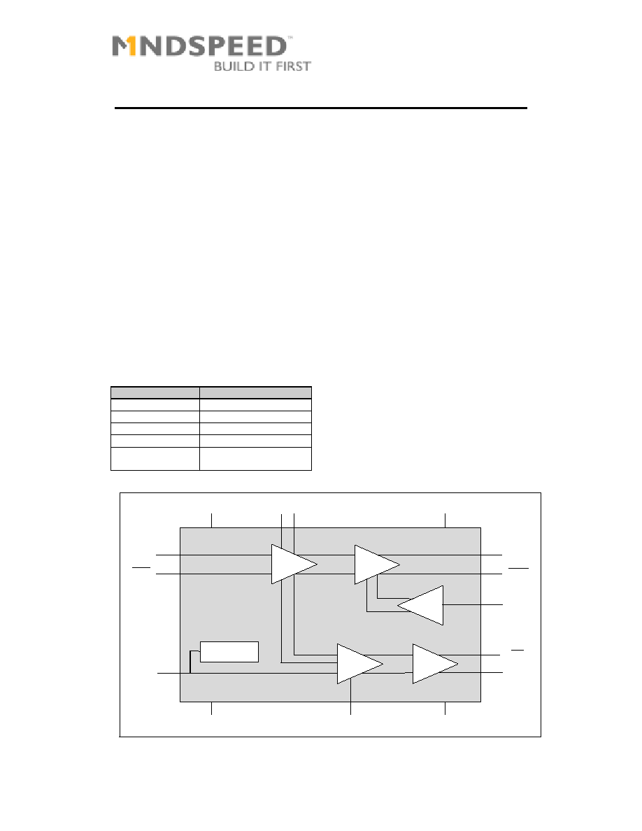
L e v e l
D e te c t
S D
B u ffe r
L im itin g
A m p .
E C L
B u ffe r
J a m
B u ffe r
R e fe re n c e
V c c A
C a z p C a z n
V c c E
G n d A
C f
G n d E
D in
D in
V s e t
D o u t
D o u t
S T
J a m
S T

MC2045-2
Preliminary Issue C
14 October, 1999
Page 2
Absolute Maximum Ratings
Symbol
Parameter
Rating
Units
P
TOT
Total power dissipation (TSSOP20)
TBA
mW
V
CC
Power
supply
(V
CC
-GND) 6
V
T
A
Operating ambient
-40 to +85
∞C
T
J
Junction
temperature
150
∞C
T
STG
Storage temperature
-65 to +150
∞C
These are the absolute maximum ratings at or beyond which the IC can be expected to fail or be damaged.
Reliable operation at these extremes for any length of time is not implied.
Recommended Operating Conditions
Symbol
Parameter
Rating
Units
V
CC
Power
supply
(V
CC
-GND)
3.0 to 5.5
V
T
A
Operating ambient
-40 to +85
∞C
DC Electrical Characteristics
Symbol
Parameter
Min
Typ
Max
Units
V
IN
Input signal voltage
1
Single-ended:
(D
IN
)
Differential:
0.8
1.6
- 400
800
mVp-p
V
OS
Input offset voltage
-
-
50
µV
V
N
Input RMS noise in 100MHz
-
-
85
µV
V
TH
Input level detect programmability
2
-
20
mVp-p
V
HYS
Level detect hysteresis (optical)
1.75
2.25
2.75
dB
I
INL
JAM input current (at 0V)
-10
-
10
µA
I
CC
Supply current (no ECL loads)
-
-
35
mA
AC Electrical Characteristics
Symbol
Parameter
Min
Typ
Max
Units
BW
Bandwidth: Lower -3dB point
Upper -3dB point
1.5 -
100
KHz
MHz
R
IN
Input
resistance
-
4.5
- k
C
IN
Input
capacitance
-
-
2 pF
T
PWD
Pulse Width Distortion
-
-
0.3
ns
T
R
,T
F
ECL out rise/fall times
(20-80% points)
- 1.0 2.0 ns
R
F
Level detect filter resistance
14
25
41
k
T
LD
Level detect time constant
0.5
1
2.0
µs
1
0.8mV is worst case sensitivity @BER10-9

MC2045-2
Preliminary Issue C
14 October, 1999
Page 3
Pin Descriptions
1
Name
Function
SOIC16
/
QSOP16
Pin #
Die
Bond #
TSSOP2
0
Pin #
C
AZN
Auto-zero capacitor pin. Connect C
AZ
between this
pin and C
AZP
.
1 1
1
C
AZP
See
C
AZN
2
2
2
GND
A
Analogue section ground pin. Connect to most
negative supply. Must be at the same potential as
GND
E
. See application diagram.
3 4
4
D
IN
Differential data input.
4
5
5
D
INB
Inverse differential data input
5
6
6
V
CCA
Analogue section power pin. Connect to most
positive supply. Must be at the same potential as
V
CCE
. See application diagram
6 3
7
C
F
Level-detect filter capacitor pin. Connect the
capacitor between here and V
CCA
7 9
8
Jam
ECL compatible input controlling D
OUT
output
buffers (Pins 12&13).
8 11 11
STb
Logical inverse of ST. Normally connected on the
PCB to Jam to enable automatic signal-threshold
function to operate.
9 12 12
ST
Input signal-level status. This ECL
2
output is LOW
when the input signal is below the threshold set by
the user. This is a differential output.
10 13 13
GND
E
Digital section ground pin. Connect to the most
negative supply. Must be at the same potential as
GND
A
. See application diagram
11 14,
15 14,
15
D
OUTB
Logical inverse of Pin 13. JAM high forces D
OUTB
high.
12 16 16
D
OUT
ECL compatible differential data output. JAM high
forces D
OUT
low.
13 17 17
V
CCE
Digital/Output section power pin. Connect to the
most positive supply. De-couple using ferrite
bead/capacitors. See diagram.
14 18,
19 18,
19
V
SET
Input threshold-level setting circuit. Connect to
analogue ground via a resistor. See application
diagram
16 20 20
NC
Not connected. Compatible with NE5224/5 PCBs.
15
3
NC
Not connected.
9, 10
1
ECL outputs are 100k compatible
Microcosm MC2044C/MC2045-2 Compatibility
The MC2044C and MC2045-2 are pin and functionally compatible, except that the MC2045-2 has
reduced bandwidth throughout, to maximise sensitivity at 155/200Mbps. In addition, the MC2044C has
CMOS-level outputs on the ST/STb pins, whereas the MC2045-2 has ECL levels.
MC2045-2
Preliminary Issue C
14 October, 1999
Page 4
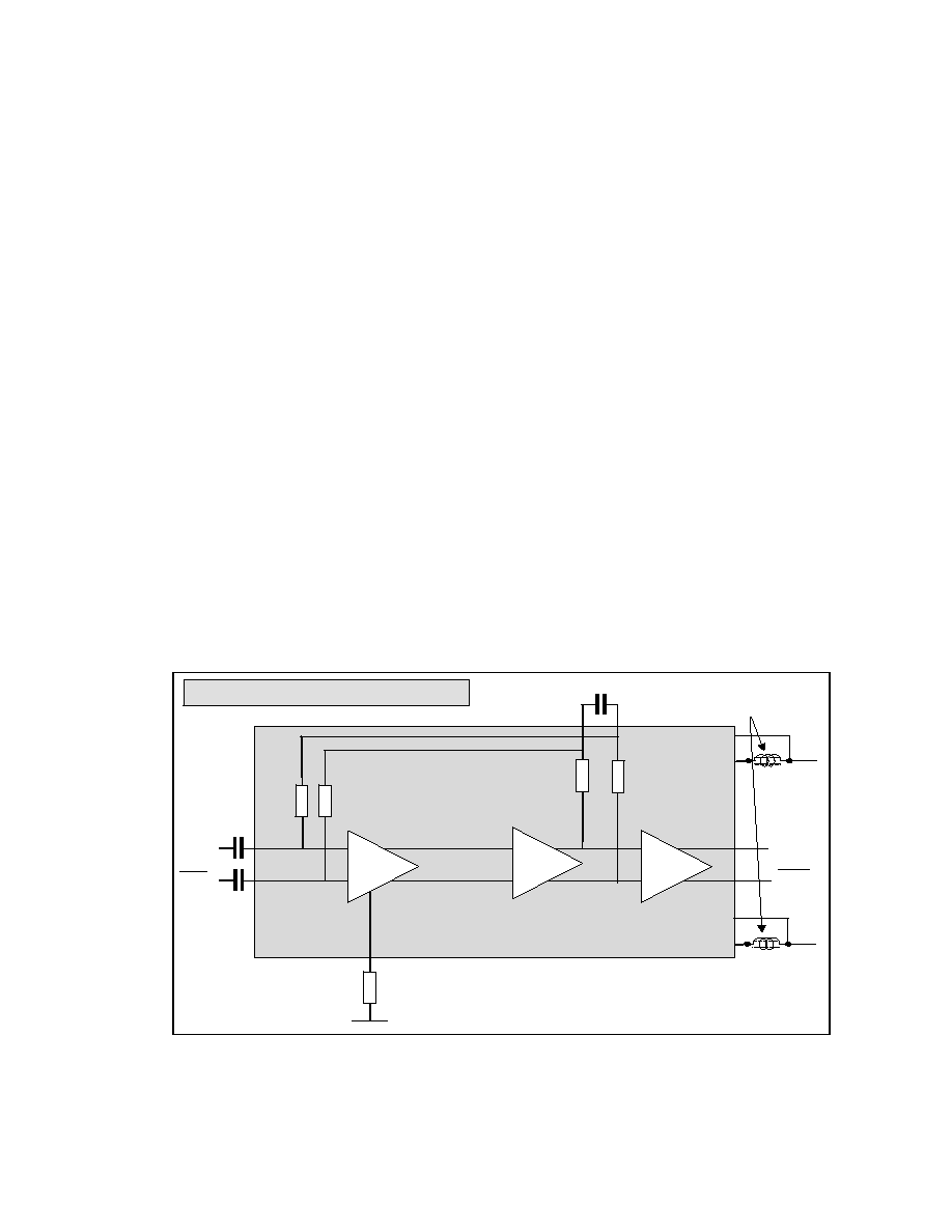
Signal Path Description
Input biasing
The Data Input pins are internally DC biased at approximately 4V, via the Rin resistors. Although the
MC2045-2 can be DC coupled, normally it will be AC coupled, using capacitors C1 & C2. Note that
Rin and C1,2 form a filter to low frequencies. The capacitors must therefore be large enough to pass the
lowest input frequencies (consecutive `1's or `0's) of interest. For example, setting C1,2 to 10nF will
give a typical -3dB point of approx. 3.5KHz.
Autozero circuit
The MC2045-2 includes an autozero circuit. In the absence of data, the feedback amplifier and
summing circuit cancel the inherent offset voltage of the signal path, keeping the comparator at its
toggle point. The time constant of this circuit is set by the combination of R
AZ
and C
AZ
, but is not
critical. C
AZ
is normally set to 10nF.
Power supply decoupling & optimising sensitivity
The MC2045-2 is not expected to require ferrite beads in order to give adequate performance.
However, if pin-compatibility with the Microcosm MC2044C is preferred, or optimum MC2045-2
sensitivity required, the V
CCA
(3) and GND
A
(6) pins of the MC2045-2 should each be connected to their
respective power rails via a BLM31A601SPT (Murata) ferrite suppressor. See the diagram, below. The
lower-cost BLM21A601SPT has not been tested, but would also be expected to work well.
Caz 10nF
Din
Dout
Dout
Rin
10k
Rin
10k
Raz
10k
Raz
10k
Din
C1
C2
Comparator
Vcc
VccA
Optional Surface-
mount Ferrite beads
VccE
Gnd
Gnd
GndE
Rset
0-2k typ.
GndA
Forward Gain Path block diagram.

MC2045-2
Preliminary Issue C
14 October, 1999
Page 5
Level detector
The MC2045-2 provides for programmable input-signal level detection, and this may be used to
automatically force the data outputs to a known state if the input signal falls below threshold. This is
normally used to allow data to propagate only when the signal is above the Bit-Error-Rate (BER)
requirement. It therefore also stops the data outputs toggling due to noise when no signal is present.
The input data is first amplified, with the level of amplification set by R
SET
, then rectified and low-pass
filtered before being compared with a reference voltage. The low-pass filter is controlled by C
F
, and
10nF will provide a nominal 1µs time constant, thus avoiding false triggering due to noise spikes.
The comparator has the equivalent of approx. 2.25dB (typ.) of optical hysteresis, operating either side
of the set level.
To complete the automatic level detect function, STb should be connected to the JAM input (See level
detect diagram, above), thus forcing the data outputs to logical zero when the signal falls below
threshold.
Note that for compatibility with the NE5224/5, Pin 15 on the SOIC16-packaged MC2045-2 is not
connected to the die (`NC'). On the NE5224/5 this pin is V
REF
, and a R1/R2 voltage divider is used to
generate V
SET
. Microcosm's solution requires only one resistor, whilst remaining compatible with the
NE5224/5.
Note that R
SET
must be connected, even if the Level-Detect function is not required.
Reference
Voltage
Din
Din
Cf 10nF
C1
C2
VccA
ST
ST
Rset
0-2k typ.
G ndA
Low-pass
Filter
Rectifier
2.2k
2.2k
G ndE
GndE
Jam
Level Detect block diagram .
Application Note on 3.3V Operation.
When running PECL at 3.3V the output pull-downs need to be lower than 300
when running into a
capacitively coupled 50ohm load.