
Preliminary Information - REV_F
May 2002
Preliminary Information
MC2045-2Y
Postamplifier/Quantizer for Applications to 200 Mbps
Data Sheet
Features
Description
Applications
Pin Descriptions
Measurement Tables
Functional Description
Features
Description
Applications
Pin Descriptions
Measurement Tables
Functional Description
Information provided in this Data Sheet is PRELIMINARY and is subject to change without
notice. MindspeedTM Technologies, Inc, Proprietary and Confidential

Preliminary Information - REV_F
Page 2 of 19
MC2045-2Y
Postamplifier/Quantizer for Applications to 200 Mbps
Preliminary Information
Information provided in this Data Sheet is PRELIMINARY and is subject to change without notice.
MindspeedTM Technologies, Proprietary and Confidential
T
ABLE
OF
C
ONTENTS
Features . . . . . . . . . . . . . . . . . . . . . . . . . . . . . . . . . . . . . . . . . . . . . . . . . . . . . . . . . . . . . . . . . . . . . . . . . . . . 3
Applications . . . . . . . . . . . . . . . . . . . . . . . . . . . . . . . . . . . . . . . . . . . . . . . . . . . . . . . . . . . . . . . . . . . . . . . . . . 3
Connections . . . . . . . . . . . . . . . . . . . . . . . . . . . . . . . . . . . . . . . . . . . . . . . . . . . . . . . . . . . . . . . . . . . . . . . . . . 3
Description . . . . . . . . . . . . . . . . . . . . . . . . . . . . . . . . . . . . . . . . . . . . . . . . . . . . . . . . . . . . . . . . . . . . . . . . . . . 3
Table 1 Ordering Information . . . . . . . . . . . . . . . . . . . . . . . . . . . . . . . . . . . . . . . . . . . . . . . . . . . . . . . . . . . . . 3
Top Level Diagram . . . . . . . . . . . . . . . . . . . . . . . . . . . . . . . . . . . . . . . . . . . . . . . . . . . . . . . . . . . . . . . . . . . . 3
Table 2 Pin Description . . . . . . . . . . . . . . . . . . . . . . . . . . . . . . . . . . . . . . . . . . . . . . . . . . . . . . . . . . . . . . . . . 4
Table 3 Absolute Maximum Ratings . . . . . . . . . . . . . . . . . . . . . . . . . . . . . . . . . . . . . . . . . . . . . . . . . . . . . . . 5
Table 4 Recommended Operating Conditions . . . . . . . . . . . . . . . . . . . . . . . . . . . . . . . . . . . . . . . . . . . . . . . 5
Table 5 DC Characteristics . . . . . . . . . . . . . . . . . . . . . . . . . . . . . . . . . . . . . . . . . . . . . . . . . . . . . . . . . . . . . . 5
Table 6 AC Characteristics . . . . . . . . . . . . . . . . . . . . . . . . . . . . . . . . . . . . . . . . . . . . . . . . . . . . . . . . . . . . . . 6
Typical Performance Curves . . . . . . . . . . . . . . . . . . . . . . . . . . . . . . . . . . . . . . . . . . . . . . . . . . . . . . . . . . . . . 7
Assert Deassert Level . . . . . . . . . . . . . . . . . . . . . . . . . . . . . . . . . . . . . . . . . . . . . . . . . . . . . . . . . . . . . . . . . . 7
Functional Block Diagram . . . . . . . . . . . . . . . . . . . . . . . . . . . . . . . . . . . . . . . . . . . . . . . . . . . . . . . . . . . . . . . 8
Functional Description . . . . . . . . . . . . . . . . . . . . . . . . . . . . . . . . . . . . . . . . . . . . . . . . . . . . . . . . . . . . . . . . . . 8
Data Input . . . . . . . . . . . . . . . . . . . . . . . . . . . . . . . . . . . . . . . . . . . . . . . . . . . . . . . . . . . . . . . . . . . . . . . . . . . 8
DC Offset Compensation . . . . . . . . . . . . . . . . . . . . . . . . . . . . . . . . . . . . . . . . . . . . . . . . . . . . . . . . . . . . . . . . 8
Signal Level Detector . . . . . . . . . . . . . . . . . . . . . . . . . . . . . . . . . . . . . . . . . . . . . . . . . . . . . . . . . . . . . . . . . . 8
Setting Signal Detect Level . . . . . . . . . . . . . . . . . . . . . . . . . . . . . . . . . . . . . . . . . . . . . . . . . . . . . . . . . . . . . . 8
Typical Applications Circuit . . . . . . . . . . . . . . . . . . . . . . . . . . . . . . . . . . . . . . . . . . . . . . . . . . . . . . . . . . . . . . 9
Applications Information . . . . . . . . . . . . . . . . . . . . . . . . . . . . . . . . . . . . . . . . . . . . . . . . . . . . . . . . . . . . . . . . 9
JAM Function . . . . . . . . . . . . . . . . . . . . . . . . . . . . . . . . . . . . . . . . . . . . . . . . . . . . . . . . . . . . . . . . . . . . . . . . . 9
PECL Termination . . . . . . . . . . . . . . . . . . . . . . . . . . . . . . . . . . . . . . . . . . . . . . . . . . . . . . . . . . . . . . . . . . . . . 9
Table 7 Termination Resistor Values . . . . . . . . . . . . . . . . . . . . . . . . . . . . . . . . . . . . . . . . . . . . . . . . . . . . . 10
Power supply de-coupling & optimizing sensitivity . . . . . . . . . . . . . . . . . . . . . . . . . . . . . . . . . . . . . . . . . . . 11
Differences between die and packaged parts . . . . . . . . . . . . . . . . . . . . . . . . . . . . . . . . . . . . . . . . . . . . . . . 11
Bare Die Information . . . . . . . . . . . . . . . . . . . . . . . . . . . . . . . . . . . . . . . . . . . . . . . . . . . . . . . . . . . . . . . . . . 12
Table 8 Pad Centers . . . . . . . . . . . . . . . . . . . . . . . . . . . . . . . . . . . . . . . . . . . . . . . . . . . . . . . . . . . . . . . . . . 12
BCC++16L Package Outline . . . . . . . . . . . . . . . . . . . . . . . . . . . . . . . . . . . . . . . . . . . . . . . . . . . . . . . . . . . 13
TSSOP20 Package Information . . . . . . . . . . . . . . . . . . . . . . . . . . . . . . . . . . . . . . . . . . . . . . . . . . . . . . . . . 14
SOIC16 Package Information . . . . . . . . . . . . . . . . . . . . . . . . . . . . . . . . . . . . . . . . . . . . . . . . . . . . . . . . . . . 15
QSOP16 Package Information . . . . . . . . . . . . . . . . . . . . . . . . . . . . . . . . . . . . . . . . . . . . . . . . . . . . . . . . . . 16
Package Dimensions . . . . . . . . . . . . . . . . . . . . . . . . . . . . . . . . . . . . . . . . . . . . . . . . . . . . . . . . . . . . . . . . . . 17
Table 9 TSSOP20 Dimensions . . . . . . . . . . . . . . . . . . . . . . . . . . . . . . . . . . . . . . . . . . . . . . . . . . . . . . . . . . 17
Table 10 SOIC16 Dimensions . . . . . . . . . . . . . . . . . . . . . . . . . . . . . . . . . . . . . . . . . . . . . . . . . . . . . . . . . . . 17
Table 11 QSOP16 Dimensions . . . . . . . . . . . . . . . . . . . . . . . . . . . . . . . . . . . . . . . . . . . . . . . . . . . . . . . . . . 17
Disclaimer . . . . . . . . . . . . . . . . . . . . . . . . . . . . . . . . . . . . . . . . . . . . . . . . . . . . . . . . . . . . . . . . . . . . . . . . . . 18
World Wide Sales Offices . . . . . . . . . . . . . . . . . . . . . . . . . . . . . . . . . . . . . . . . . . . . . . . . . . . . . . . . . . . . . . 19

Preliminary Information - REV_F
Page 3 of 19
MC2045-2Y
Postamplifier/Quantizer for Applications to 200 Mbps
Preliminary Information
Information provided in this Data Sheet is PRELIMINARY and is subject to change without notice.
MindspeedTM Technologies, Proprietary and Confidential
F
EATURES
Low-cost IC, fabricated in advanced sub-micron BiCMOS
process
800
�
V input sensitivity
Wide range programmable input-signal level detect
Fully differential design
Supports 3.3 V and 5 V supplies
Available in TSSOP20, SOIC16, QSOP16 and
BCC++16L package as well as die form
Complimentary PECL data & signal detect logic outputs
A
PPLICATIONS
SDH/SONET/ATM
Fast Ethernet
FDDI
ESCON
FTTH and Media Converters
C
ONNECTIONS
D
ESCRIPTION
The MC2045-2Y is an integrated, high gain limiting
amplifier intended for fibre optic communication to
200 Mbps. Normally placed following the photodetector &
transimpedance amplifier, the post-amplifier provides the
necessary gain to give PECL compatible logic outputs.
The MC2045-2Y also includes a programmable signal-
level detector, allowing the user to set thresholds at which
the logic outputs are enabled. The signal detect function
has typically 2 dB (optical) of hysteresis which prevents
chatter at low input levels.
A JAM function, which turns off the output when no signal
is present, is provided by externally connecting the ST
output to the JAM input.
T
ABLE
1
O
RDERING
I
NFORMATION
T
OP
L
EVEL
D
IAGRAM
Microcosm
MC2045-2Y
Date Code
1
2
3
4
5
6
7
8
16
15
14
13
12
11
10
9
C
AZ
-
C
AZ
+
GndA
D
IN
V
CC
A
C
F
JAM
D
IN
V
SET
NC
V
CC
E
D
OUT
GndE
ST
ST
D
OUT
Microcosm
MC2045-2Y
Date Code
1
2
3
4
5
6
7
8
9
10
20
19
18
17
16
15
14
13
12
11
C
AZ
-
C
AZ
+
NC
G ndA
D
IN
D
IN
V
CC
A
C
F
NC
NC
V
SET
V
C C
E
V
C C
E
D
OU T
D
OU T
G ndE
G ndE
ST
ST
JAM
1
2
3
4
5
6
7
8
9
10
11
12
13
14
15
16
V
CC
A
D
IN
D
IN
JA
M
ST
ST
GndE
D
OUT
D
OUT
V
CC
E
C
AZ
+
C
AZ
-
V
SET
Cf
V
CC
A
NC
BCC++ Top View
GndA
Fig. 1
SOIC16
QSOP16
Package
TSSOP20
Package
BCC++16
Package
Part Number
Pin Package
MC2045-2YDIEWP
Waffle pack
MC2045-2YWAFER
Expanded wafer on a grip ring
MC2045-2YS16
SOIC16
MC2045-2YQ16
QSOP16
MC2045-2YT20
TSSOP20
MC2045-2Y-06-T
BCC++16L
M02045-2-BEVM
BCC16 evaluation board
M02045-2-QEVM
QSOP evaluation board
M02045-P6EVM
QSOP Eval board inc. MC2006 TIA
M02045-P7EVM
QSOP Eval board inc. MC2007 TIA
D
IN
D
OUT
D
OUT
GndE
GndE
V
CCE
V
CCE
V
SET
C
AZ
-
C
AZ
+
V
CC
A
GndA
ST
JAM
V
SET
C
F
Level
Detector
GndA
V
CC
A
ST
D
IN
Fig. 2

Preliminary Information - REV_F
Page 4 of 19
MC2045-2Y
Postamplifier/Quantizer for Applications to 200 Mbps
Preliminary Information
Information provided in this Data Sheet is PRELIMINARY and is subject to change without notice.
MindspeedTM Technologies, Proprietary and Confidential
T
ABLE
2
P
IN
D
ESCRIPTION
Note :
Pin 17 (center pin) on the BCC++16 package should be connected to GndA.
Pin
Name
QSOP16
SOIC16
Pin No.
TSSOP20
Pin No.
BCC++16L
Pin No
Function
C
AZ
-
1
1
15
Auto-zero capacitor pin. Connect C
AZ
between this pin and C
AZ
+
C
AZ
+
2
2
16
Auto-zero capacitor pin. Connect C
AZ
between this pin and C
AZ
-
GNDA
3
4
-
Analog section ground pin. Connect to most negative supply.Must be at the
same potential as GNDE pin
D
IN
4
5
2
Differential data input
D
IN
5
6
3
Inverse differential data input
V
CCA
6
7
1, 4
Analog section power pin. Connect to most positive supply.Must be at the
same potential as V
CC
E pin
C
F
7
8
5
Level-detect filter capacitor pin. Connect a capacitor between this pin and
V
CC
A
JAM
8
11
6
PECL compatible input controlling output buffers (D
OUT
and D
OUT
pins).
On chip pull down defaults to low. Can be driven from CMOS.
ST
9
12
7
Logical inverse of ST pin. Maybe connected to JAM pin to enable
automatic squelch function to operate PECL output
ST
10
13
8
Input signal level status. This PECL output is LOW when the input signal is
below the threshold set by the users
GNDE
11
14, 15
10
Digital section ground pin, Connect to the most negative supply. Must be
the same potential as GNDA pin
D
OUT
12
16
11
Differential data output. Logical inverse of D
OUT
pin. JAM high forces D
OUT
High
D
OUT
13
17
12
Differential data output. PECL compatible differential data output. JAM high
forces D
OUT
LOW
V
CCE
14
18, 19
13
Digital output section power pin. Connect the most positive supply. Must be
at same potential as V
CCA
pin.
NC
15
3, 9, 10
9
Not connected
V
SET
16
20
14
Input threshold-level setting circuit. Connect to GND via a resistor
Preliminary Information - REV_F
Page 5 of 19
MC2045-2Y
Postamplifier/Quantizer for Applications to 200 Mbps
Preliminary Information
Information provided in this Data Sheet is PRELIMINARY and is subject to change without notice.
MindspeedTM Technologies, Proprietary and Confidential
T
ABLE
3
A
BSOLUTE
M
AXIMUM
R
ATINGS
These are the absolute maximum ratings at or beyond which the IC can be expected to fail or be damaged. Reliable
operation at these extremes for any length of time is not implied.
T
ABLE
4
R
ECOMMENDED
O
PERATING
C
ONDITIONS
T
ABLE
5
DC C
HARACTERISTICS
(V
CC
= +3.3V
�
10%, T
A
= -40�C to +85�C, unless otherwise noted)
1) Load is 50
to V
CC
-2 V.
2) VCC = +3.3 V or +5 V.
Symbol
Parameter
Rating
Units
V
CC
Power supply (V
CC
-GND)
6
V
T
A
Operating ambient
-40 to +85
�C
T
STG
Storage temperature
-65 to +150
�C
Symbol
Parameter
Rating
Units
V
CC
Power supply (V
CC
-GND)
3.0 to 5.5
V
T
A
Operating ambient
-40 to +85
�C
Symbol
Parameter
Min.
Typ.
Max.
Units
V
OS
Effective input offset voltage
-
1
-
mV
V
TH
Input level detect programmability
2
-
20
mVpp
HYS
Level detect hysteresis (optical)
1.8
2.0
3.0
dB
I
INJ
JAM input current HIGH
380
�A
I
CC
Supply current (outputs un-loaded)
(2)
-
-
20
mA
V
OH
PECL
(1)
output HIGH
V
CC
-1.025
-
V
CC
-0.880
V
V
OL
PECL
(1)
output LOW
V
CC
-1.810
-
V
CC
-1.620
V

Preliminary Information - REV_F
Page 6 of 19
MC2045-2Y
Postamplifier/Quantizer for Applications to 200 Mbps
Preliminary Information
Information provided in this Data Sheet is PRELIMINARY and is subject to change without notice.
MindspeedTM Technologies, Proprietary and Confidential
T
ABLE
6
AC C
HARACTERISTICS
(V
CC
= +3.3 V
�
10%, T
A
= -40�C to +85�C, unless otherwise noted)
Symbol
Parameter
Min.
Typ.
Max.
Units
BW
Bandwidth (where gain = 60dB)
100
250
-
MHz
R
IN
Input resistance
-
4.5
-
k
C
IN
Input capacitance
-
-
2
pF
t
PWD
Pulse width distortion
-
-
0.3
ns
t
R
,t
F
Data output rise/fall times (20-80%)
-
1.0
2.0
ns
R
F
Signal level detect filter resistance
10
25
41
k
T
LD
Signal level detect time constant
Assert level
Deassert level
0.5
1
50
20
�s
V
IN
Input signal voltage
Single ended:
Differential :
0.8
1.6
-
-
400
800
mVpp
V
N
Input RMS noise in 100 MHz
-
-
85
�V

Preliminary Information - REV_F
Page 7 of 19
MC2045-2Y
Postamplifier/Quantizer for Applications to 200 Mbps
Preliminary Information
Information provided in this Data Sheet is PRELIMINARY and is subject to change without notice.
MindspeedTM Technologies, Proprietary and Confidential
T
YPICAL
P
ERFORMANCE
C
URVES
A
SSERT
D
EASSERT
L
EVEL
The Fig. 3a shows the operation of the signal detect
function as the signal level varies. The top line indicates
the assert level, the bottom the deassert level. The
difference between the two levels is the hysteresis. When
the signal level goes above the assert level the ST output
switches high (ST switches low). When the signal level
falls below the deassert level, ST output switches low (ST
switches high).
T yp ical Sig nal D etect (At 25�C and 5.0V)
0.0
5.0
10.0
15.0
20.0
25.0
0
600
1200
1800
Vi
n
(
m
Vp
-
p
)
Assert
D eassert
R
SE T
(
)
T yp ical Sig nal D etect (At 25�C and 3.3V)
0.0
5.0
10.0
15.0
20.0
25.0
30.0
0
600
1200
1800
Vi
n
(
m
Vp
-
p
)
Assert
D eassert
R
S ET
(
)
ST
Signal Input Lev el
Assert Lev el
D eassert Lev el
ST
H y steresis
Fig. 3
Fig. 3a

Preliminary Information - REV_F
Page 8 of 19
MC2045-2Y
Postamplifier/Quantizer for Applications to 200 Mbps
Preliminary Information
Information provided in this Data Sheet is PRELIMINARY and is subject to change without notice.
MindspeedTM Technologies, Proprietary and Confidential
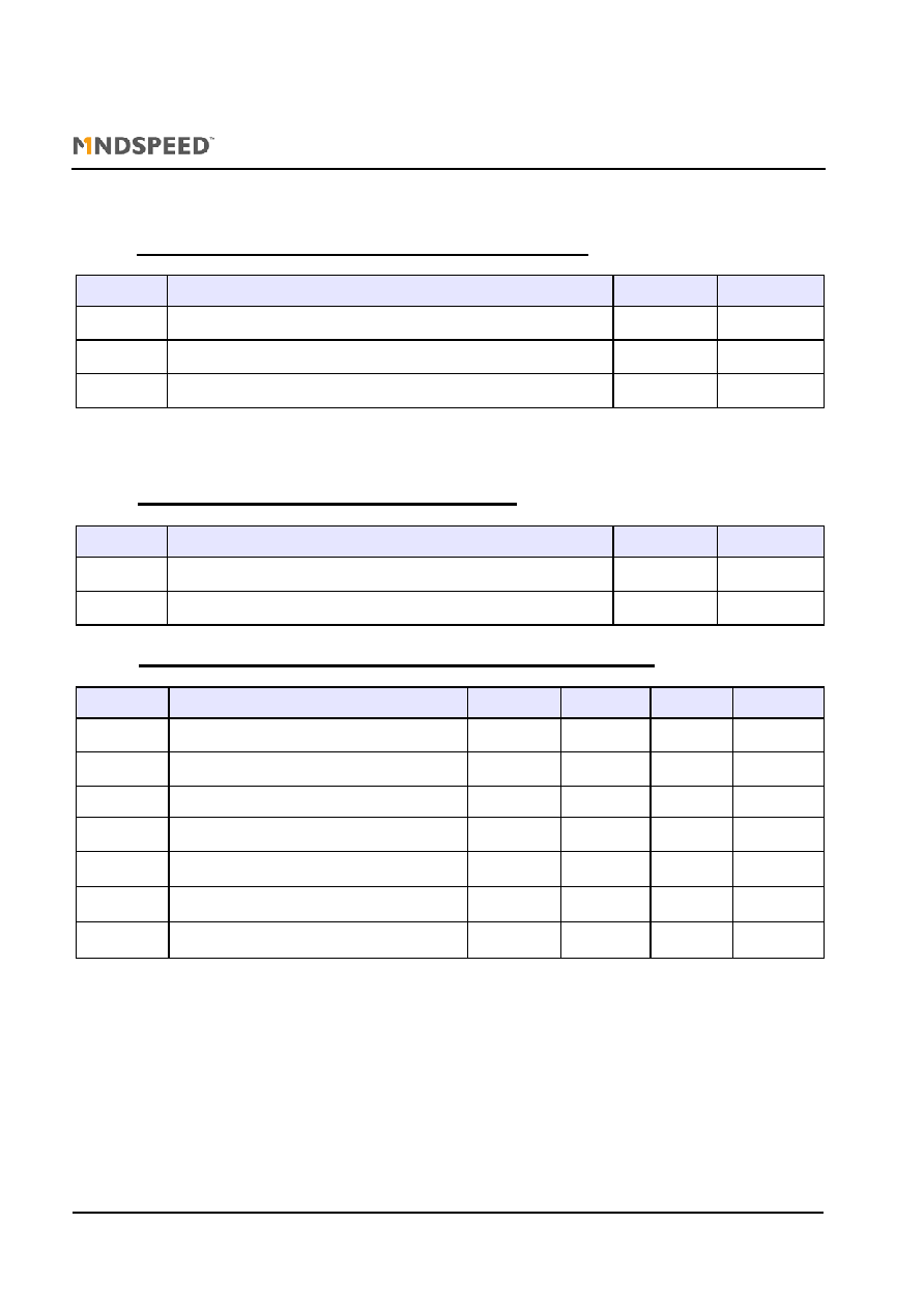
F
UNCTIONAL
B
LOCK
D
IAGRAM
F
UNCTIONAL
D
ESCRIPTION
Data Input
The Data Input pins are internally DC-biased at
approximately V
CC
-1V. The MC2045-2Y signals are AC
coupled, using external capacitors. These capacitors
must be large enough to pass the lowest frequencies of
interest (consecutive `1's or `0's) considering the input
resistance. For example, at 155 Mbps SONET, there can
be up to a maximum of 72 consecutive `1' s, which is
465 ns.
To minimise the data dependant jitter, the low frequency
cut-off needs to be lower by a factor of 10. However, it is
better to set it a further decade lower, due to the
interaction of the time constants for the input stage and
the DC restore circuitry. For example setting C1, C2 (Fig.
5) to 10 nF will give a typical -3 dB point of approximately
3.5 KHz.
DC Offset Compensation
Internal feedback is included to remove the effects of DC
offsets and acts as a DC auto zero circuit. An external
capacitor (C
AZ
) acting with the internal circuit feedback
resistors (typ 10 k
) ensures that the feedback is
effective only at frequencies below the lowest frequency
of interest. C
AZ
is normally set to 10 nF.
Signal Level Detector
The gain of the first stage is determined by R
SET
. This
amplification sets the level of input at which the status
thresholds operate. The data is then rectified and low-
pass filtered before being compared with a reference
voltage. The low-pass filter is formed by C
F
(Fig. 5) and
R
F
(on chip resistor).
With C
F
equal to 10 nF the time constant is nominally
2 �s, avoiding false triggering due to variation in edge
density of data.
Setting Signal Detect Level
R
SET
is chosen using the graphs in Fig. 3 to determine the
input signal level at which ST goes high (Assert). The
value is dependant on supply voltage and should be
chosen for 3.3 V or 5 V operation. If 3.3 V and 5 V
operation are to be supported inter-changeably set RSET
based on the 3.3 V graphs.
The comparator following the level detector has the
equivalent of 2 dB (typ.) of optical hysteresis, and this
detemines the deassert level (ST goes LOW).
If the level detect function is not required connect V
SET
to
GndA (maximum gain).
Level
D etector
V
C C A
C
F
V
C C E
ST
ST
JAM
D
O U T
D
O U T
C
AZ
+
C
A Z
-
V
S ET
G ndE
G ndA
D
IN
D
IN
10K
10K
10K
10K
Fig. 4
Preliminary Information - REV_F
Page 9 of 19
MC2045-2Y
Postamplifier/Quantizer for Applications to 200 Mbps
Preliminary Information
Information provided in this Data Sheet is PRELIMINARY and is subject to change without notice.
MindspeedTM Technologies, Proprietary and Confidential
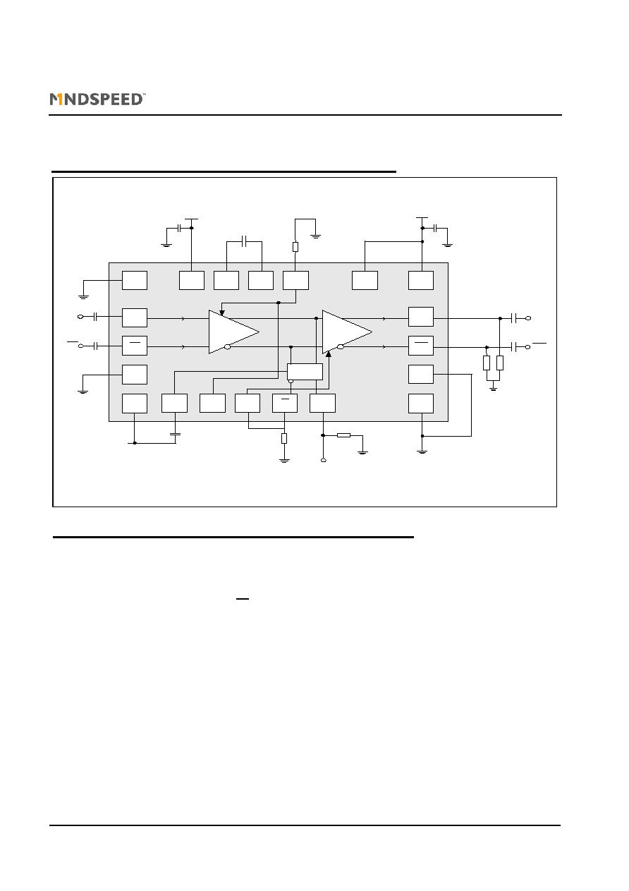
T
YPICAL
A
PPLICATIONS
C
IRCUIT
A
PPLICATIONS
I
NFORMATION
JAM Function
The JAM function, sets the data output to a fixed state
when no valid signal is present at the input. This is
implemented by externally connecting the ST output to
the JAM input.
This is normally used to allow data to propagate only
when the signal is above the users' Bit-Error-Rate (BER)
requirement. It therefore stops the data outputs toggling
due to noise when no signal is present.
PECL Termination
The outputs of the MC2045-2Y are PECL compatible and
any standard AC or DC-coupling termination technique
can be used. Fig. 6 and 7 illustrate typical AC and DC
terminations.
AC-coupling is used in applications where the average
DC content of the data is zero e.g. SONET. The
advantage of this approach is lower power consumption,
no susceptibility to DC drift and compatibility with non
PECL interfaces. Pull-down resistors (R
pull-down
) provide
a DC path for the emitter follower outputs to Gnd, keeping
the ECL output transistors in their active region. Values
for R
pull-down
, at different supply voltages, can be found in
table 7.
DC-coupling can be used when driving PECL interfaces
and has the advantage of a reduced component count. A
Thevenin termination is used at the receive end to give a
50
load and the correct DC bias. Fig. 7 shows the
circuit configuration and table 7 the resistor values.
Alternatively, if available, terminating to V
CC
�2V as
shown in Fig. 8 (page 11) has the advantage that the
resistance value is the same for 3.3 V and 5 V operation
and it also has performance advantages at high data
rates.
When calculating ZT the impedance of the transmission
line (Z) must be taken into consideration.
D
IN
D
IN
V
C C
V
C C
In F
C 1
D
O U T
D
O U T
2 .2 k
S T
2 .2 k
C F
R
S E T
D
IN
D
O U T
D
O U T
G n d E
G n d E
V
C C E
V
C C E
V
S E T
C
A Z
-
C
A Z
+
V
C C
A
G n d A
S T
J A M
V
S E T
C
F
L e ve l
D e te c to r
G n d A
V
C C
A
S T
D
IN
C 2
2 2 n F
C A Z
*
* O p tio n a l c o n n e c t io n t o e n a b le J A M f u n c tio n
V C C
R P ull-dow n
0 .1 � F
0 .1 � F
R P ull-dow n
Fig. 5
Preliminary Information - REV_F
Page 10 of 19
MC2045-2Y
Postamplifier/Quantizer for Applications to 200 Mbps
Preliminary Information
Information provided in this Data Sheet is PRELIMINARY and is subject to change without notice.
MindspeedTM Technologies, Proprietary and Confidential
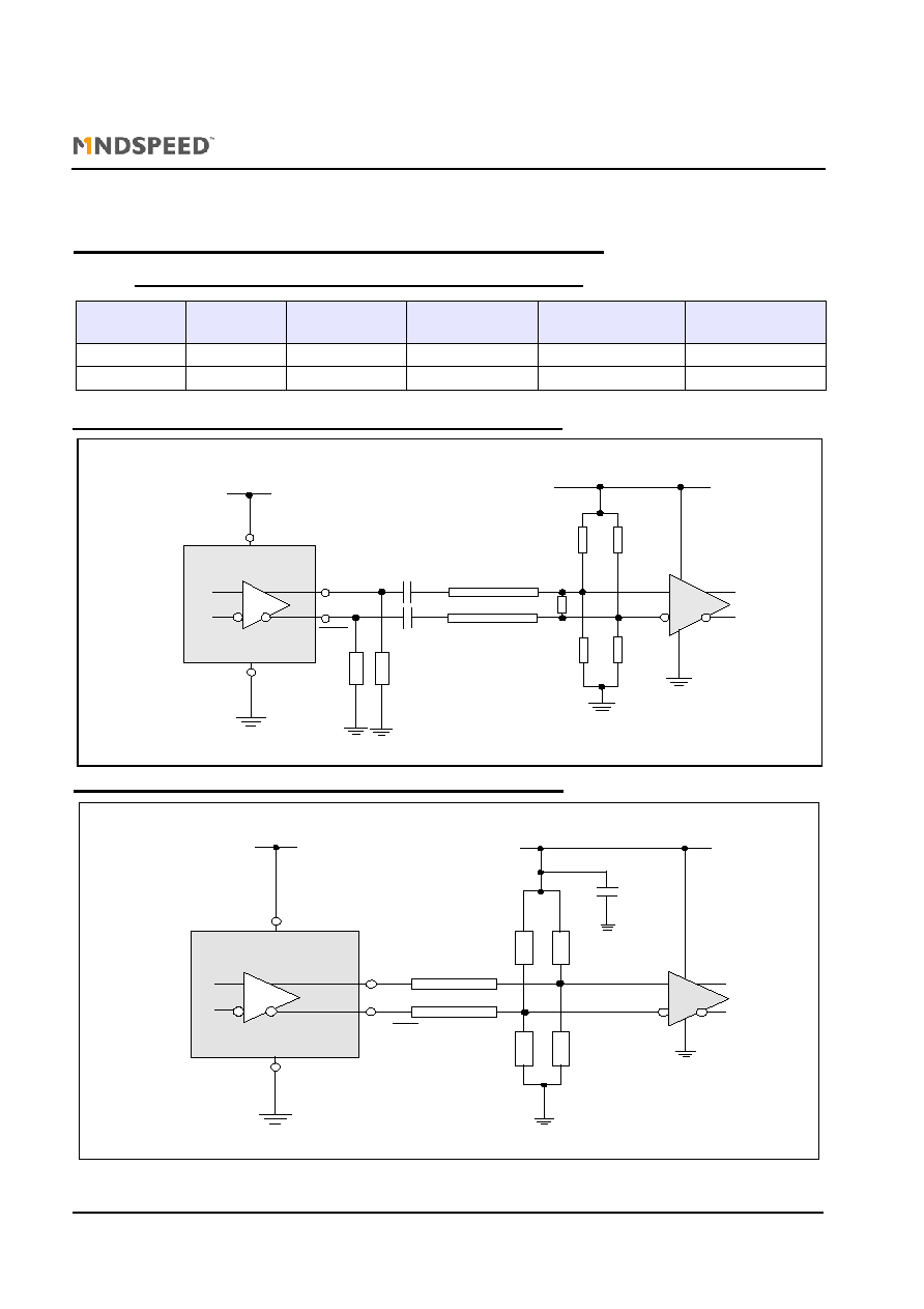
A
PPLICATIONS
I
NFORMATION
T
ABLE
7
T
ERMINATION
R
ESISTOR
V
ALUES
AC-C
OUPLED
PECL T
ERMINATION
DC-C
OUPLED
PECL T
ERMINATION
Supply
Output
Impedance
R
Pull-down
Z
T
R
TA
/R
TB
R
T
/R
B
5 V
50
270
100
2k7
/7k8
82
/130
3.3 V
50
150
100
2k7
/4k3
130
/82
V
CC
2045-2Y
D
OUT
D
OUT
Z
Z
ZT
R
pull-down
PECL
0.1�F
V
CC
RTA
RTB
0.1�F
RTB
RTA
Fig. 6
V
C C
2 0 4 5 -2 Y
V
C C
D
OUT
D
OUT
R
B
R
T
1 0 n F
Z
Z
P E C L
Fig. 7
Preliminary Information - REV_F
Page 11 of 19
MC2045-2Y
Postamplifier/Quantizer for Applications to 200 Mbps
Preliminary Information
Information provided in this Data Sheet is PRELIMINARY and is subject to change without notice.
MindspeedTM Technologies, Proprietary and Confidential
A
PPLICATIONS
I
NFORMATION
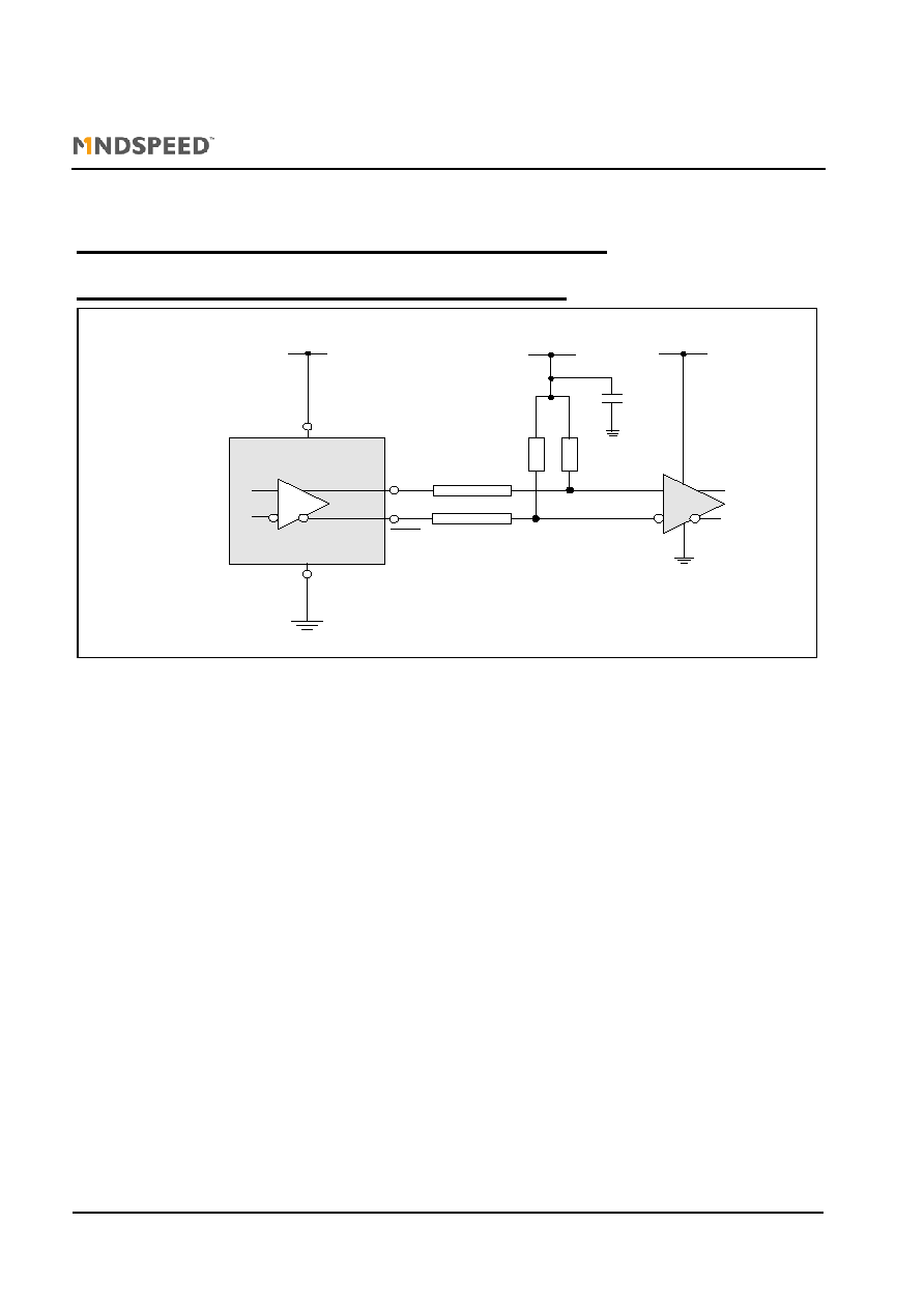
A
LTERNATIVE
PECL T
ERMINATION
Power supply de-coupling & optimizing
sensitivity
In most applications the MC2045-2Y will give adequate
performance without ferrite beads. In applications where
maximum sensitivity is required V
CC
A and GNDA may be
connected to their respective power rails via a ferrite
suppressor, such as a Murata BLM31A601SPT.
Capacitors should be chosen with low effective series
resistance, low dissipation factor and high Q. NPO or
COG temperature characteristics are preferred because
they provide more reliable performance over a wide range
of environmental conditions.
Small surface mount packages are recommended since
they exhibit less parasitic inductance which can lower the
overall effectiveness of the bypass capacitor at high
frequencies. Filter capacitors should be placed close to
power and ground pins to minimise noise coupling.
Differences between die and packaged
parts
The die has two V
SET
pads. Connect one or other, not
both.
There are 2 sets of V
CC
A and GNDA on the left of the die.
Although two pairs are provided only one pair need be
connected. On the TSSOP package, pairs of V
CC
E and
GNDE pins are connected.
V
CC
2045-2Y
V
CC
-2 V
D
OUT
D
OUT
50
10nF
Z
Z
V
CC
PECL
50
Fig. 8

Preliminary Information - REV_F
Page 12 of 19
MC2045-2Y
Postamplifier/Quantizer for Applications to 200 Mbps
Preliminary Information
Information provided in this Data Sheet is PRELIMINARY and is subject to change without notice.
MindspeedTM Technologies, Proprietary and Confidential
B
ARE
D
IE
I
NFORMATION
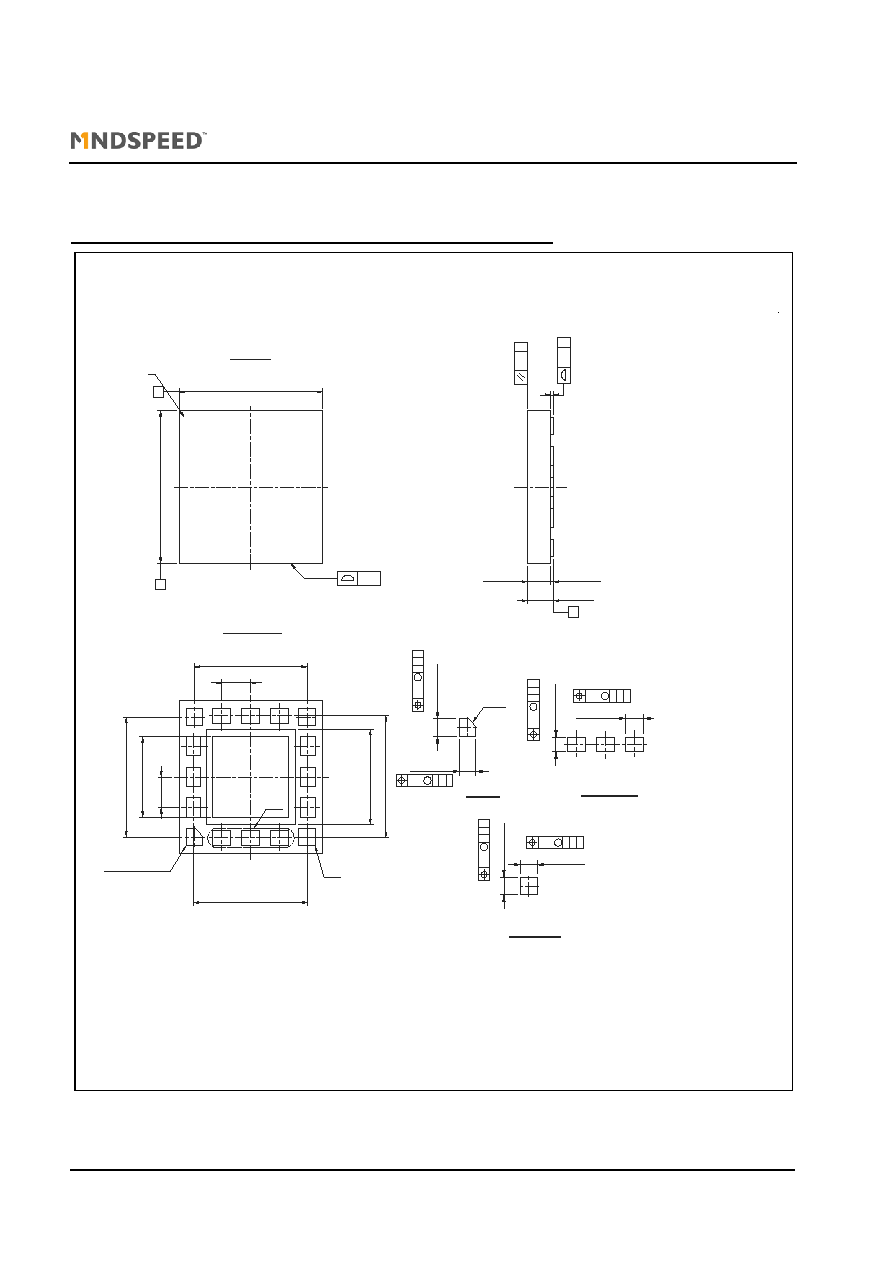
T
ABLE
8
P
AD
C
ENTERS
Note: Pad coordinates are in
�m, and are measured from the center of the die to the center of the pad.
Description
X
Y
Description
X
Y
C
AZ
-
-56.8
347.5
JAM
-152.2
-347.5
C
AZ
+
-207
347.5
ST
15.8
-347.5
V
CC
A1
-356.9
347.5
ST
166
-347.5
GNDA1
-670
322.6
GNDE1
670
-248
D
IN
-670
172.6
GNDE2
670
-103
D
IN
-670
22.4
D
OUT
670
50.1
GNDA2
-670
-127.6
D
OUT
670
200.3
V
CC
A2
-670
-277.5
V
CC
E1
670
347.5
C
F
-451.4
-347.5
V
CC
E2
436.9
347.5
V
SET2
-301.3
-347.5
V
SET
93.2
347.5
GNDA1
D
IN
V
CC
A2
CF
V
SE
T
JA
M
ST
GNDE1
D
OUT
V
CC
E2
V
SE
T
GNDA2
D
IN
ST
GNDE2
D
OUT
V
CC
E1
V
CC
A1
C
AZ
+
C
AZ
-
Fig. 9
Pad size : 85 x 85
�m
Die thickness : 300
�m �10%
Preliminary Information - REV_F
Page 13 of 19
MC2045-2Y
Postamplifier/Quantizer for Applications to 200 Mbps
Preliminary Information
Information provided in this Data Sheet is PRELIMINARY and is subject to change without notice.
MindspeedTM Technologies, Proprietary and Confidential
BCC++16L P
ACKAGE
O
UTLINE
TOP VIEW
BOTTOM VIEW
0.15
X
M
ZY
0.
08
0.
05
Z
0.
20 Z
Z
Y
X
0.45
0.
45
X
M Z
Y
0.08
DETAIL "A"
0.
4
0
0.50
X
M
ZY
0.
08
X
M Z
Y
0.08
DETAIL "B" (12X)
DETAIL "C" (3X)
0.45
0.
4
5
X
M Z
Y
0.08
MZ
0.
08
XY
4.
00
�
0.
10
4.00 � 0.10
0.67 � 0.025
0.075 � 0.025
0.80 MAX
"B"
"C"
C.L(PKG.)
C.
L
(
P
K
G
.
)
C0.2
"A"(PIN 1 CORNER)
(PIN 1 CORNER)
3.
20
3.15
3.
15
3.20
0.
80
�
0.
10
0.80 � 0.10
2.
50
�
0.
1
0
2.
10
�
0.
1
0
+0
.
0
5
-0
.
0
3
-0.03
+0.05
-0
.
0
3
+0
.
0
5
-0.03
+0.05
+0.05
-0.03
+0
.
0
5
-0
.
0
3
Fig. 10
Preliminary Information - REV_F
Page 14 of 19
MC2045-2Y
Postamplifier/Quantizer for Applications to 200 Mbps
Preliminary Information
Information provided in this Data Sheet is PRELIMINARY and is subject to change without notice.
MindspeedTM Technologies, Proprietary and Confidential
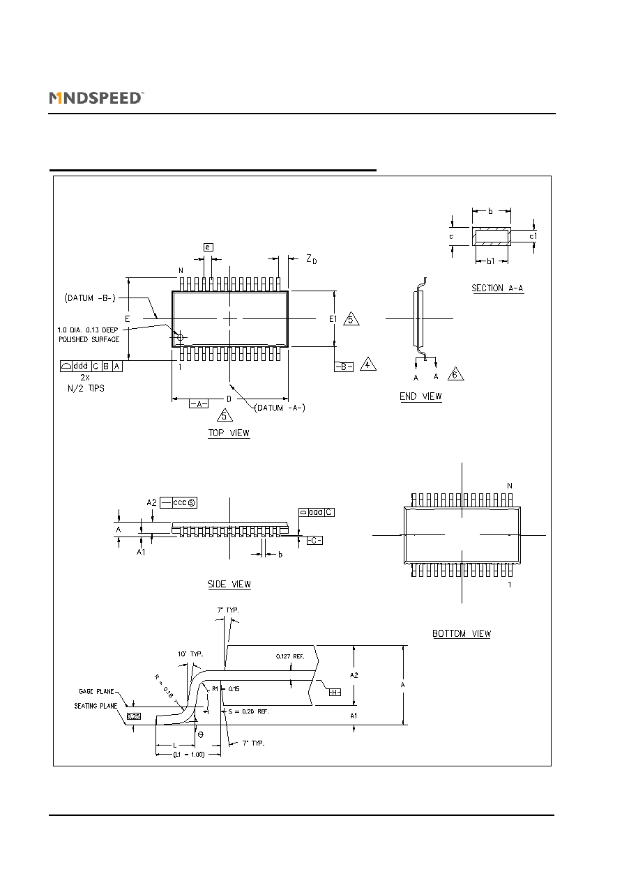
TSSOP20 P
ACKAGE
I
NFORMATION
Note: Please see dimensions on page 17, table 9.
Fig.11
Preliminary Information - REV_F
Page 15 of 19
MC2045-2Y
Postamplifier/Quantizer for Applications to 200 Mbps
Preliminary Information
Information provided in this Data Sheet is PRELIMINARY and is subject to change without notice.
MindspeedTM Technologies, Proprietary and Confidential
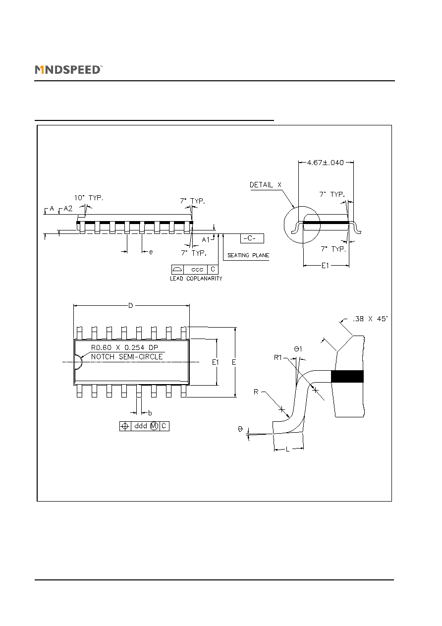
SOIC16 P
ACKAGE
I
NFORMATION
Note: Please see dimensions on page 17, table 10.
Fig. 12

Preliminary Information - REV_F
Page 16 of 19
MC2045-2Y
Postamplifier/Quantizer for Applications to 200 Mbps
Preliminary Information
Information provided in this Data Sheet is PRELIMINARY and is subject to change without notice.
MindspeedTM Technologies, Proprietary and Confidential
QSOP16 P
ACKAGE
I
NFORMATION
Note: Please see dimensions on page 17, table 11.
Fig.13

Preliminary Information - REV_F
Page 17 of 19
MC2045-2Y
Postamplifier/Quantizer for Applications to 200 Mbps
Preliminary Information
Information provided in this Data Sheet is PRELIMINARY and is subject to change without notice.
MindspeedTM Technologies, Proprietary and Confidential
P
ACKAGE
D
IMENSIONS
T
ABLE
9
TSSOP20 D
IMENSIONS
T
ABLE
10
SOIC16 D
IMENSIONS
T
ABLE
11
QSOP16 D
IMENSIONS
Dims.
Tols/leads
TSSOP20L
A
MAX
1.20
A1
0.5MIN/.10MAX.
A2
NOM
.90
D
�.05
6.50
E
�.10
6.40
E1
�.10
4.40
L
+.15/-.10
.60
L1
REF.
1.00
Zp
REF.
.325
e
BASIC
.65
b
�.05
.22
c
.13MIN/.20MAX
e
�4�
4�
aaa
MAX.
.10
bbb
MAX.
.10
ccc
MAX
.05
ddd
MAX.
.20
Dims.
Tols/N
SOIC16
A
MAX.
1.70
A1
�.05
0.17
A2
�.10
1.38
D
�.10
9.9
E
�.20
6.00
E1
�.10
3.90
L
�.05
0.5
ccc
MAX.
0.10
ddd
MAX.
0.10
e
BASIC
1.27
b
�.05
0.43
O
0�~7�
01
�4�
7�
R
MAX
0.20
R1
TYP.
0.13
Dims.
Tols/N
QSOP16
A
MAX.
1.60
A1
�.05
0.1
A2
�.10
1.40
D
�.10
4.9
E
�.20
6.00
E1
�.10
3.90
L
�.05
0.6
ccc
MAX.
0.10
ddd
MAX.
0.10
e
BASIC
0.65
b
�.05
0.25
c
�.05
.2 Min.
.24 Max.
R
�.05
0.20
R1
Min.
0.20

MC2045-2Y
Preliminary Information - REV_F
Page 18 of 19
Postamplifier/Quantizer for Applications to 200 Mbps
Preliminary Information
Information provided in this Data Sheet is PRELIMINARY and is subject to change without notice.
MindspeedTM Technologies, Proprietary and Confidential
D
ISCLAIMER
� 2001 Mindspeed TechnologiesTM, as a wholly owned subsidiary and the Internet infrastructure business of Conexant
Systems, All Rights are Reserved.
Information in this document is provided in connection with Mindspeed Technologies. "Mindspeed" products. These
materials are provided by Mindspeed as a service to its customers and may be used for informational purposes only.
Mindspeed assumes no responsibility for errors or omissions in these materials. Mindspeed may make changes to
specifications and product descriptions at any time, without notice. Mindspeed makes no commitment to update the
information contained herein. Mindspeed shall have no responsibility whatsoever for conflicts or incompatibilities arising
from future changes to its specifications and product descriptions.
No license, express or implied, by estoppel or otherwise, to any intellectual property rights is granted by this document.
Except as provided in Mindspeed Terms and Conditions of Sale for such products, Mindspeed assumes no liability
whatsoever.
THESE MATERIALS ARE PROVIDED "AS IS" WITHOUT WARRANTY OF ANY KIND, EITHER EXPRESS OR IMPLIED,
RELATING TO SALE AND/OR USE OF CONEXANT PRODUCTS INCLUDING LIABILITY OR WARRANTIES RELATING
TO FITNESS FOR A PARTICULAR PURPOSE, MERCHANTABILITY, OR INFRINGEMENT OF ANY PATENT,
COPYRIGHT OR OTHER INTELLECTUAL PROPERTY RIGHT. Mindspeed further does not warrant the accuracy or
completeness of the information, text, graphics or other items contained within these materials. Mindspeed shall not be
liable for any special, indirect, incidental, or consequential damages, including without limitation, lost revenues or lost
profits, which may result from the use of these materials.
Mindspeed products are not intended for use in medical, life saving or life sustaining applications. Mindspeed customers
using or selling Mindspeed products for use in such applications do so at their own risk and agree to fully indemnify
Mindspeed for any damages resulting from such improper use or sale.
The following are trademarks of Mindspeed Technologies,. the symbol M1, MindspeedTM, and "Build It FirstTM" Product
names or services listed in this publication are for identification purposes only, and may be trademarks of third parties.
Third-party brands and names are the property of their respective owners.
Reader Response: Mindspeed Technologies, strives to produce quality documentation and welcomes your feedback.
Please send comments and suggestions to mailto:tech.pubs@mindspeed.com. For technical questions, or to talk to a field
applications engineer contact your local MindspeedTM sales office listed below. For literature send email request to
literature@mindspeed.com.

Preliminary Information - REV_F
Page 19 of 19
Americas
US Northwest/Northwest Canada
Santa Clara
Phone: (408) 423-4500
Fax: (408) 249-7113
US North Central
Illinois/Colorado
Phone: (630) 799-9300
Fax: (630) 799-9325
US South Central
Texas
Phone: (972) 735-1540
Fax: (972) 407-0639
Eastern Canada
Ontario
Phone: (613) 271-2358
Fax: (613) 271-2359
US Northeast
Massachusetts
Phone: (978) 244-7680
Fax: (978) 244-6868
US Southeast
North Carolina
Phone: (919) 858-9110
Fax: (919) 858-8669
US Florida / South America
Florida
Phone: (727) 799-8406
Fax: (727) 799-8306
US Mid-Atlantic
Pennsylvania
Phone: (215) 245-2470
Fax: (215) 245-2480
Asia
P.R. China - Central and North
Australia and New Zealand
Phone: (86-21) 6350-5702
Fax: (6-21) 6361-2516
P.R. China - South/Hong Kong
Phone: 86-755-2300-420
Fax: 86-755-2300-421
Asia South - Taiwan
India, Indonesia, Malaysia, Pakistan,
Philippines, Singapore, Taiwan, Thailand
and Vietnam
Phone: (886-2) 8789-8366
Fax: (886-2) 8789-8367
Korea
Phone: 82-2-528-4301
Fax: 82-2-528-4305
Japan
Phone: (81-3) 5380 1731
Fax: (81-3) 5350-5431
Europe
Europe Central - Germany
Austria, Germany, Hungary, Poland,
Romania, Russia and Switzerland
Phone: (49) 89-82005-151
Fax: (49) 89-82005-150
Europe Mediterranean - Israel
Greece, Israel, Italy, Spain and Portugal
Phone: (972) 9961-5100
Fax: (972) 9957 5166
Europe North - UK
Belgium, Denmark, Finland, France, Ireland
Luxembourg, Norway, Sweden,
The Netherlands and United Kingdom
Phone: 44 (0) 118 920 9500
Fax: 44 (0) 118 920 9595
Headquarters
Newport Beach
Mindspeed Technologies
4000 MacArthur Boulevard, East Tower
Newport Beach, CA 92660
Phone: (949) 579-3000
Fax: (949) 579-3020
www.mindspeed.com
World Wide Sales Offices
Information provided in this Data Sheet is PRELIMINARY and is subject to change without notice.
MindspeedTM Technologies, Proprietary and Confidential