Preliminary
ML0308
ML0308 Backlight LED
Boost Converter
The ML0308 is a step-up DC-DC converter specifically
designed to drive up to four white LEDs in series from a single
lithium-ion cell. The device provides regulated and inherently
matched current to the LEDs with additional functions:
automatic soft-start, output overvoltage protection, ON/OFF
and dimming control. The ML0308 switches at 1.0 MHz,
featuring the use of tiny external components.
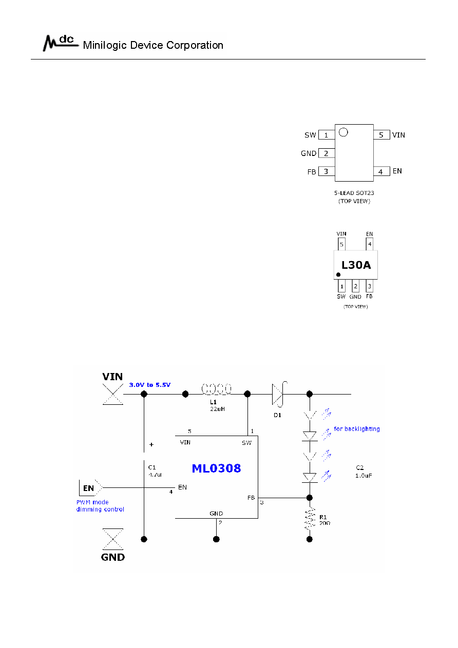
PACKAGE INFORMATION
Features
Inherently-matched LED
current
Drives up to four white LEDs
from 3.6V supply
Automatic soft-start
Output overvoltage protection
High efficiency
Applications
LED backlighting with
dimming control
High efficiency step-up
converter
MARKING DIAGRAM
Figure 1: Typical application circuit

Preliminary
ML0308
ABSOLUTE MAXIMUM RATINGS
Rating Pin
Value
Unit
Input voltage
VIN
6.0
V
Output voltage
SW
18
V
EN
10
V
FB
VIN+0.3
V
Operating temperature
-30 to 80
�C
Storage temperature
-40 to 125
�C
ELECTICAL CHARACTISTICS
All specifications apply under the condition V
IN
= 3.0V and T
A
= 25�C unless specified.
The donates the specifications which apply over the full operating temperature range
PARAMETER CONDITIONS MIN
TYP
MAX
UNITS
Minimum Operating Voltage
3.0
V
Maximum Operating Voltage
5.5 V
Feedback Voltage
0�C to 85�C
185
200
215 mV
Supply Current
Switching
EN Pin = 0V
100
150
0.1
uA
uA
EN Pin HIGH Threshold
1.2 V
EN Pin LOW Threshold
0.5
V
Switch Frequency
0.7
1.0
1.53 MHz
Duty Ratio
73
75
77 %
MOSFET Current Limit
180
250
mA
MOSFET ON Resistance
V
IN
=3.0V, I
DS
= 100mA
MOSFET Leakage Current
V
IN
=5.5V
1.0 uA
Overvoltage Limit
16.7
17.5 V
Soft-start Time
200
us
Preliminary
ML0308
PIN FUNCTION DESCRIPTION
Pin Description
SW (Pin 1)
This pin is the power side of the external inductor and must be connected to the external
Schottky diode. It provides the output current to the load. Since the boost converter
operates in a current loop mode, the output voltage can range up to 16V but shall not
exceed this limit.
GND (Pin 2)
This pin is the system ground for the ML0308 and carries both the power and the analog
signals. High quality ground must be provided to avoid spikes and/or uncontrolled
operation. Care must be observed to avoid high-density current flow in a limited PCB
copper track so arobust ground plane connection is recommended.
FB (Pin 3)
This pin provides the output current range adjustment by means of a sense resistor
connected to the internal analog control circuitry.
EN (Pin 4)
This pin is the chip-enable Pin. Ground this pin to shutdown the chip. Apply a clock
with different duty ratio to control brightness of the LEDs.
VIN (Pin 5)
The external voltage supply is connected to this pin. A high quality reservoir capacitor
must be connected across pin 5 and Ground to achieve the specified output voltage
parameters. A 4.7uF/6.3 V, low ESR capacitor must be connected as close as possible
across pin 5 and ground pin 2.
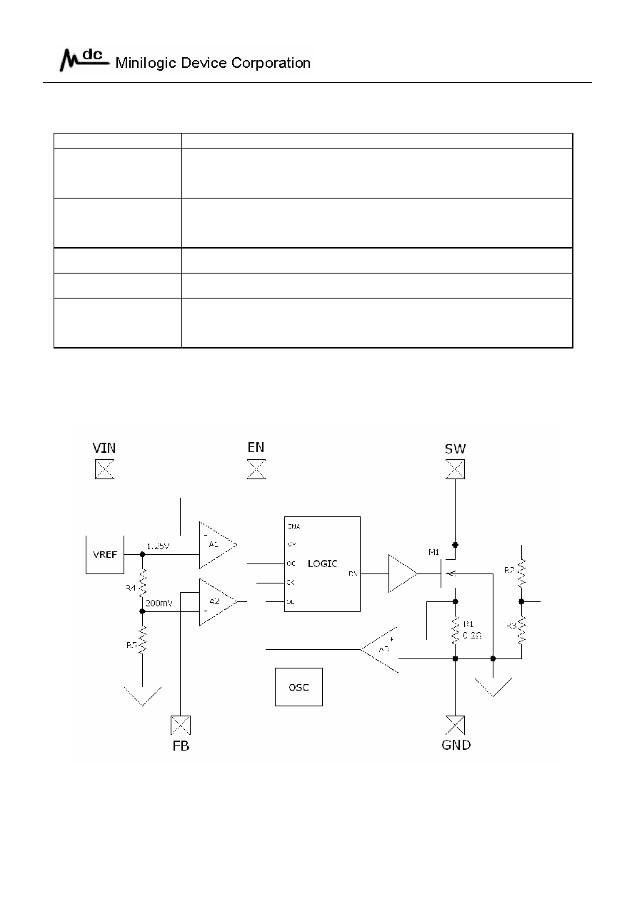
INTERNAL BLOCK DIAGRAM
Figure 2: Internal block diagram

Preliminary
ML0308
THEORY OF OPERATION
The ML0308 uses a PFM, current mode control scheme to provide excellent line and load regulation.
Its operation can be best explained with reference to figure 2 and figure 1. The oscillator generates a
clock of 1.0MHz with 75% duty ratio for the main control logic. When EN pin goes HIGH, the power
MOSFET switches at 1.0 MHz to drive the LED current up to the target level. When the inductor
current reaches the limit, comparator A3 will toggle and the MOSFET will stop charging the inductor
until the inductor current falls below the limit. Therefore, soft-start is achieved and potential hazards
from explosive startup are avoided. When LED current reaches and rises over the regulation point,
feedback voltage at FB pin will raise over 200mV and comparator A2 toggles. The chip will then stop
switching the MOSFET until LED current falls below the threshold. Therefore, LED current is
regulated and the threshold.
HISTORY OF REVISION
REV DESCRIPTION
DATE
PRE0 Preliminary
Release
12/03/2004
PRE1 Preliminary
Release1
18/08/2004
DISCLAIMER:
The information presented in this document does not form part of any quotation or contract, is believed to be accurate and
reliable and may be changed without notice. No liability will be accepted by the publisher for any consequence of its use.