Page 2
ML62 Series
Positive Voltage Regulator
v
Application
u Battery Powered Equipment
u Palmtops
u Portable Cameras and Video Recorders
u Reference Voltage Sources
v
Features
l CMOS Low Power Consumption :
Typical 3.3uA at Vout=5.0V
l Output Voltage Range : 2.0V to 6.0V in 0.1V increments
l Highly Accurate : Output Voltage + 2%
l Maximum Output Current: 250mA
(within the maximum power dissipation , Vout=5.0V)
l Small Input-Output Voltage Differential :
0.12V at 100mA and 0.38V at 200mA
l Input stability : Typ. 0.2%/V
l Package Available :
SOT- 23 (150mW), SOT- 89 (500mW) & TO - 92
(300mW)
v
Absolute Maximum Ratings
Parameter
Symbol
Ratings
Units
Input Voltage
V
IN
12
V
Output Current
I
OUT
500
mA
Output Voltage
V
OUT
V
SS
-0.3 ~V
IN
+0.3
V
SOT-23
150
SOT-89
500
Continuous
Total Power
Dissipation
TO-92
P
d
300
mW
Operating Ambient
Temperature
T
opr
-30 ~ +70
o
C
Storage Temperature
T
stg
-30 ~ +70
o
C
v
General Description
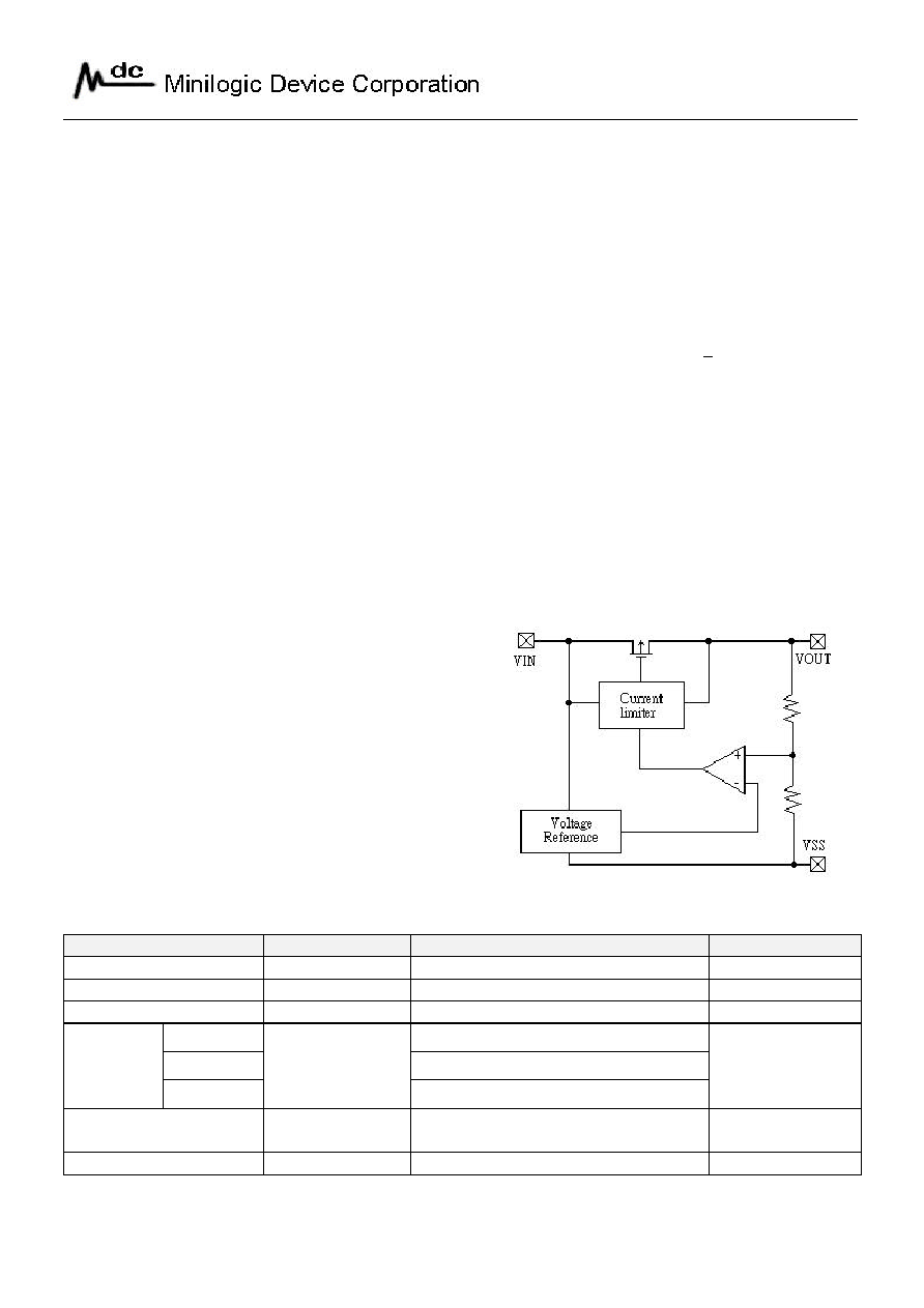
The ML62 is a group of positive voltage output,
three-pin regulator which provides high output
current even when the input/output voltage
differential is small.
The ML62 consists of a high-precision voltage
reference, an error correction circuit, and a current
limited output driver.
v
Block Diagram
Page 4
v
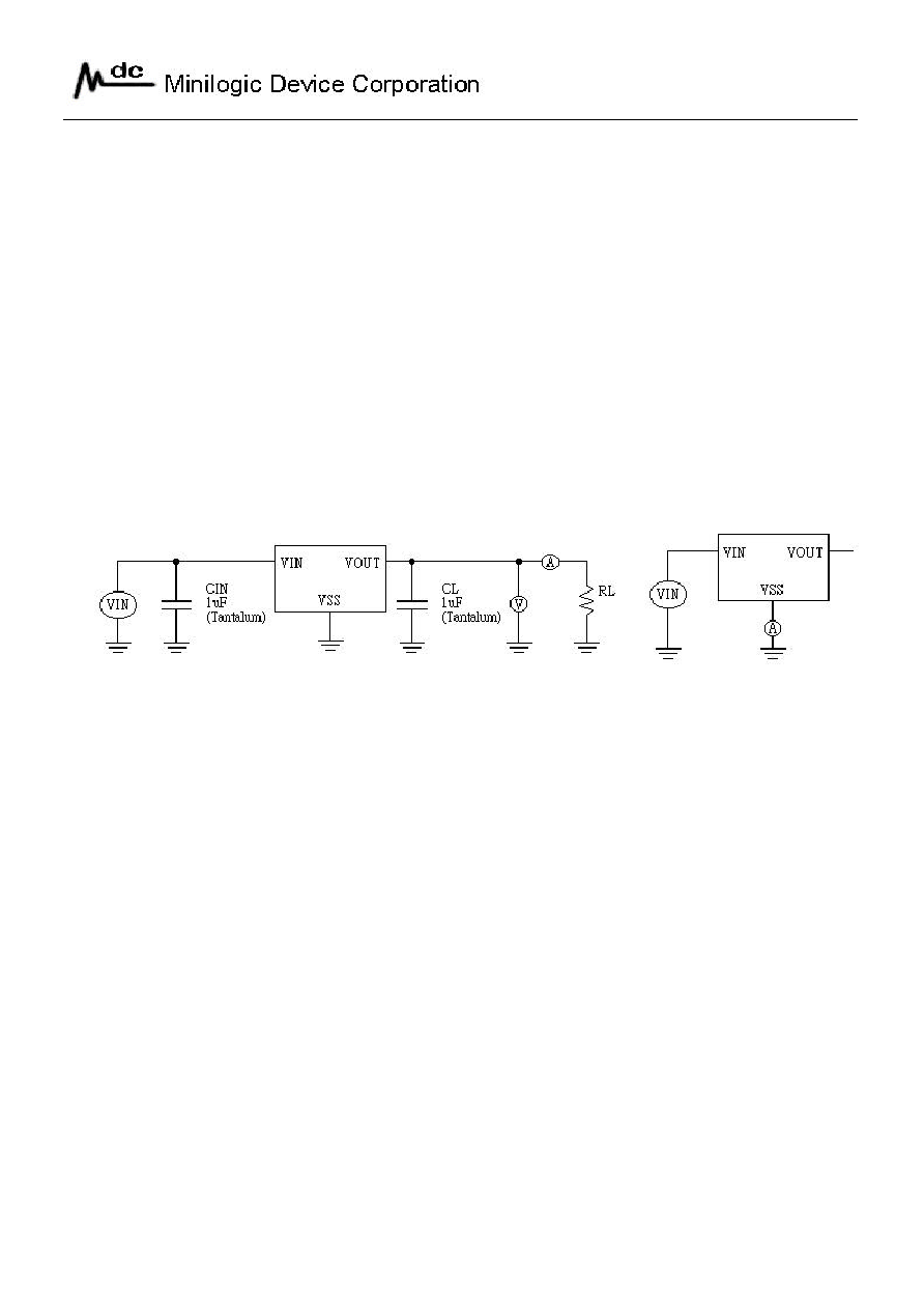
Standard Circuit
Note on Use
1. Oscillation may occur as a result of the impedance present between the power supply and the IC's input. Please use a
capacitor (CIN) of at least 1uF, when the impedance is 10 ohm or more.
With a large output current, Voltage output can be stabilised by increasing capacitor (CIN) size. If CIN is small and
capacitor (CL) size is increased, oscillation may occur. In such cases, Voltage output can be stabilised by either increasing
the size of CIN or decreasing the size of CL.
2. Please ensure that output current (IOUT) is less than Pd / (VIN-VOUT) and does not exceed the stipulated Continuous Total
Power Dissipation value (Pd).
v
Test Circuit
Test Circuit 1
Test Circuit 2
Page 5
v
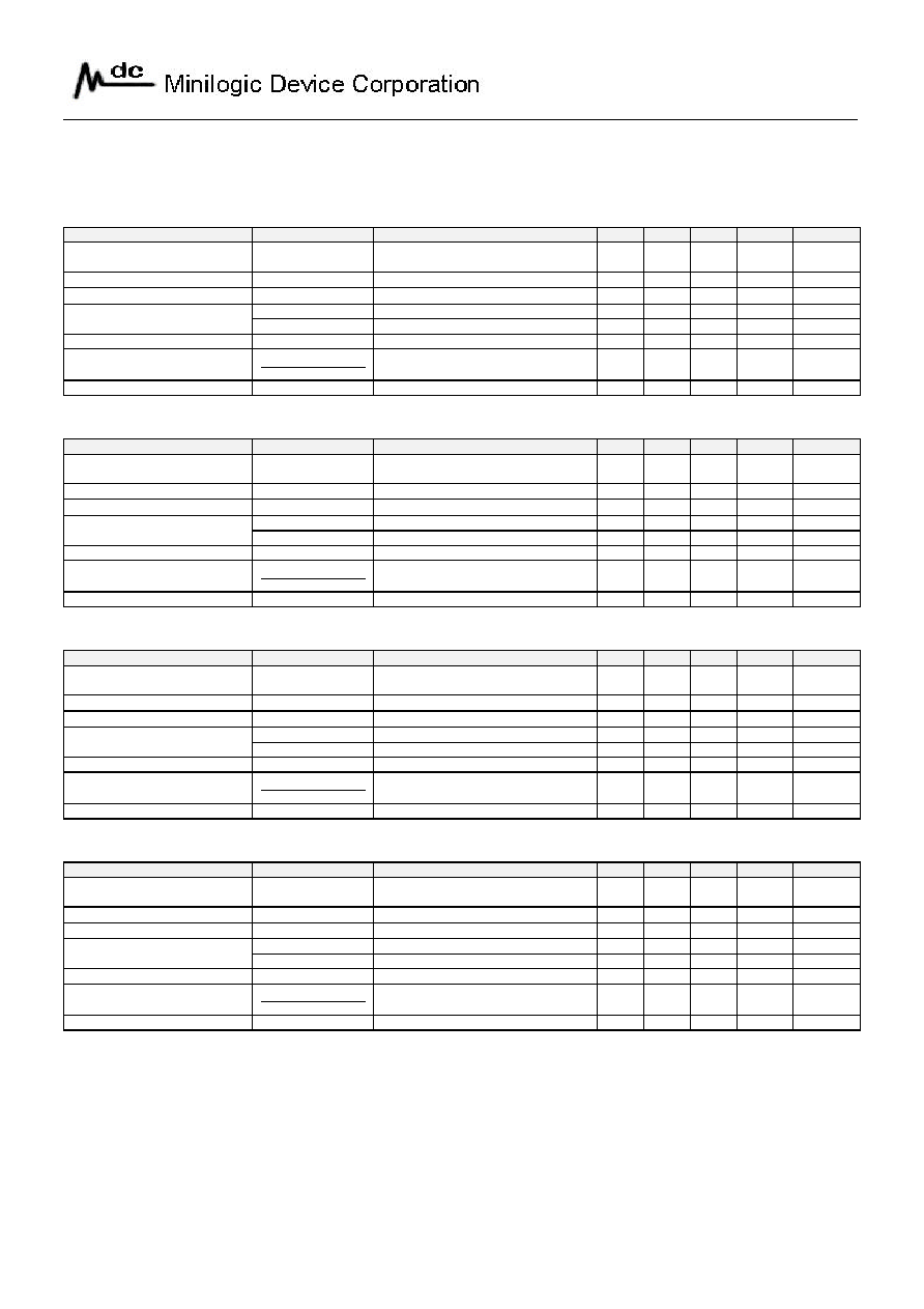
Electrical Characteristics
ML62502 V
OUT
(T)=5.0V(Note 1)
Parameter
Symbol
Conditions
Min
Typ
Max
Units
Circuit
Output Voltage
VOUT(E)
(Note 2)
IOUT=40mA
VIN=6.0V
4.900 5.000 5.100
V
1
Maximum Output Current
IOUT max
VIN=6.0V, VOUT(E)
4.5V
250
mA
1
Load Stability
VOUT
VIN=6.0V, 1mA
IOUT
100mA
40
80
mV
1
Vdif1
IOUT=100mA
120
400
mV
1
Input ≠Output
Voltage Differential (Note 3)
Vdif2
IOUT=200mA
380
750
mV
1
Supply Current
ISS
VIN=6.0V
3.3
4.5
uA
2
Input Stability
VOUT
VIN * VOUT
IOUT=40mA
6.0V
VIN
10.0V
0.2
0.3
%V
1
Input Voltage
VIN
10
V
-
ML62402 V
OUT
(T)=4.0V(Note 1)
Parameter
Symbol
Conditions
Min
Typ
Max
Units
Circuit
Output Voltage
VOUT(E)
(Note 2)
IOUT=40mA
VIN=5.0V
3.920 4.000 4.080
V
1
Maximum Output Current
IOUT max
VIN=5.0V, VOUT(E)
3.6V
200
mA
1
Load Stability
VOUT
VIN=5.0V, 1mA
IOUT
100mA
45
90
mV
1
Vdif1
IOUT=90mA
170
400
mV
1
Input ≠Output
Voltage Differential (Note 3)
Vdif2
IOUT=180mA
400
750
mV
1
Supply Current
ISS
VIN=5.0V
3.0
4.5
uA
2
Input Stability
VOUT
VIN * VOUT
IOUT=40mA
5.0V
VIN
10.0V
0.2
0.3
%V
1
Input Voltage
VIN
10
V
-
ML62302 V
OUT
(T)=3.0V(Note 1)
Parameter
Symbol
Conditions
Min
Typ
Max
Units
Circuit
Output Voltage
VOUT(E)
(Note 2)
IOUT=40mA
VIN=4.0V
2.940 3.000 3.060
V
1
Maximum Output Current
IOUT max
VIN=4.0V, VOUT(E)
2.7V
150
mA
1
Load Stability
VOUT
VIN=4.0V, 1mA
IOUT
80mA
45
90
mV
1
Vdif1
IOUT=80mA
180
450
mV
1
Input ≠Output
Voltage Differential (Note 3)
Vdif2
IOUT=150mA
400
850
mV
1
Supply Current
ISS
VIN=4.0V
2.8
4.5
uA
2
Input Stability
VOUT
VIN * VOUT
IOUT=40mA
4.0V
VIN
10.0V
0.2
0.3
%V
1
Input Voltage
VIN
10
V
-
ML62202 V
OUT
(T)=2.0V(Note 1)
Parameter
Symbol
Conditions
Min
Typ
Max
Units
Circuit
Output Voltage
VOUT(E)
(Note 2)
IOUT=40mA
VIN=3.0V
1.960 2.000 2.040
V
1
Maximum Output Current
IOUT max
VIN=3.0V, VOUT(E)
1.8V
100
mA
1
Load Stability
VOUT
VIN=3.0V, 1mA
IOUT
60mA
45
90
mV
1
Vdif1
IOUT=60mA
180
450
mV
1
Input ≠Output
Voltage Differential (Note 3)
Vdif2
IOUT=100mA
400
850
mV
1
Supply Current
ISS
VIN=3.0V
2.5
4.5
uA
2
Input Stability
VOUT
VIN * VOUT
IOUT=40mA
3.0V
VIN
10.0V
0.2
0.3
%V
1
Input Voltage
VIN
10
V
-
Note : 1. VOUT(T) = Specified Output Voltage.
2. VOUT(E) = Effective Output Voltage (i.e. the output voltage when (VOUT(T)+1.0V) is provided at the VIN pin
while maintaining a certain IOUT value).
3. Vdif = VIN1(Note 4) ≠ VOUT(E)
4. VIN1 = The input voltage at the time 98% of VOUT (E) is output (input voltage has been gradually reduced).

