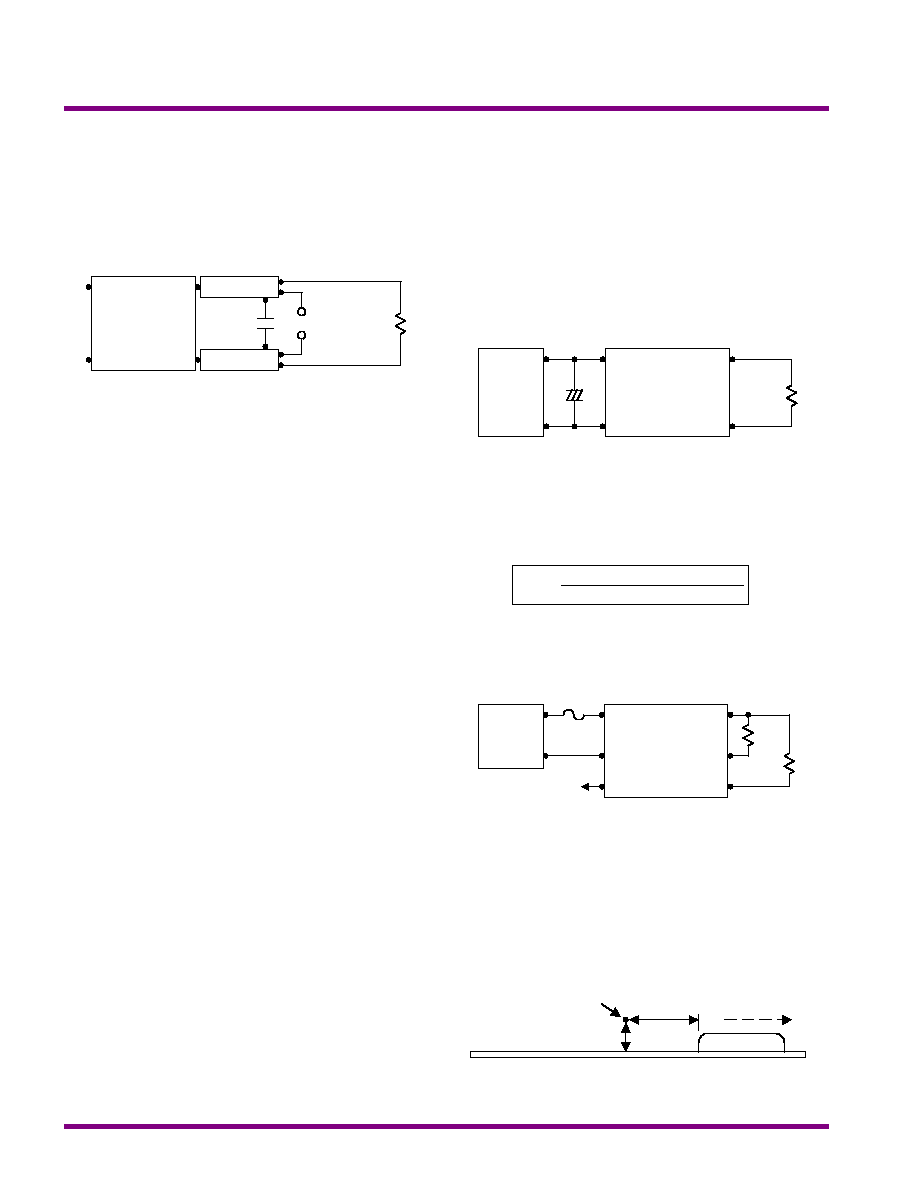
Single Output
Switching
Regulator
+Vin
-Vin
On/Off
+Vo
Adj.
-Vo
Block Diagram
More Power
High
Power
Density
Vout Adj.
Low Noise
Remote on/off
Wide Range
3:1
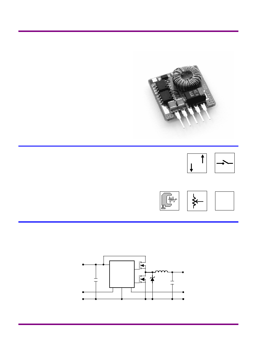
High efficiency, wide input voltage range and low output noise define
Minmax's IDS Series of non-isolated, step-down, switching DC/DC
converters.
The 3.3V and 5V output devices are respectively up to 93% efficiency.
All models are fully line and load regulated and maintain specified accuracy
over the impressively wide input voltage ranges of 4.75 to 13.6V for 3.3V
output, 6 to 16.5V for 5V output and 16 to 28V for 3.3V and 5V outputs.
Output ripple and noise are typically 30mV P-P.
The high efficiency of the IDS Series eliminates the need for thermally
conductive potting compound. Devices are specified for full-power operation
up to ambient temperatures of +70] Calculated MTBF (MIL-HDBK-217F)
is more than 1.5 million hours.
These simple-to-use power converters have no minimum load
requirements. They draw 1mA when unloaded and a mere 100uA in the
standby mode (On/Off Control turns off).
3.3V models have an output voltage adjustment range from 1.8 to 3.3V
and 5V models are adjustable down to 3.0V.
Standby Current 100uA only
Overload Protection
Step-down Switching Regulator
Temperature Performance -25] to +70]
Low Output Noise
Remote On/Off Control
Low Cost
MTBF > 1,500,000 Hours
Output Current up to 2A
Efficiency up To 93%
Key Features
10W, Step-Down, Single Output DC/DC Converters
IDS100 Series
REV:0 2005/04
MINMAX
1

85
490
200
2000
5
IDS122
83
45
331
200
2000
3.3
24
( 16 ~ 28 )
IDS121
93
27
896
200
2000
5
12
( 6 ~ 16.5 )
IDS112
92
21
1434
200
2000
3.3
5
( 4.75 ~ 13.6 )
IDS101
% (Typ.)
mA (Typ.)
mA (Typ.)
mA
mA
VDC
VDC
@Max. Load
@No Load
@Max. Load
Min.
Max.
Efficiency
Input Current
Output Current
Output
Voltage
Input
Voltage
Model
Number
Model Selection Guide
Free-Air Convection
Cooling
%
95
---
Humidity
]
+125
-25
Storage Temperature
]
+70
-25
Ambient
Operating Temperature
Unit
Max.
Min.
Conditions
Parameter
Environmental Specifications
Exceeding the absolute maximum ratings of the unit could cause damage.
These are not continuous operating ratings.
mW
1500
---
Internal Power Dissipation
]
235
---
Lead Temperature (1.5mm from case for 10 Sec.)
VDC
30
-0.7
24VDC Input Models
VDC
25
-0.7
12VDC Input Models
VDC
16
-0.7
5VDC Input Models
Input Surge Voltage
( 1000 mS )
Unit
Max.
Min.
Parameter
Notes :
1. Specifications typical at Ta=+25], resistive load,
nominal input voltage, rated output current unless
otherwise noted.
2. Transient recovery time is measured to within 1%
error band for a step change in output load of 50%
to 100%.
3. Ripple & Noise measurement bandwidth is 0-20
MHz.
4. These power converters require a minimum
output loading to maintain specified regulation.
5. Operation under no-load conditions will not
damage these modules; however, they may not
meet all specifications listed.
6. All DC/DC converters should be externally fused at
the front end for protection.
7. Other input and output voltage may be available,
please contact factory.
8. Specifications subject to change without notice.
Absolute Maximum Ratings
15
---
12
24V Input Models
6
---
5.5
12V Input Models
VDC
3.9
---
3.5
5V Input Models
Start Voltage
Unit
Max.
Typ.
Min.
Model
Parameter
Input Specifications
IDS100 Series
2
MINMAX
REV:0 2005/04

Continuous
Output Short Circuit
%/]
{0.02
{0.01
---
Temperature Coefficient
%
{4
{2
---
Transient Response Deviation
uS
150
100
---
50% Load Step Change
Transient Recovery Time
%
---
---
120
Over Load
mV rms
15
---
---
Ripple & Noise (20MHz)
mV P-P
120
---
---
Over Line, Load & Temp.
Ripple & Noise (20MHz)
mV P-P
50
30
---
Ripple & Noise (20MHz)
%
{1.5
{0.5
---
Io=0% to 100%
Load Regulation
%
{0.5
{0.2
---
Vin=Min. to Max.
Line Regulation
%
{2.0
{1.0
---
Output Voltage Accuracy
Unit
Max.
Typ.
Min.
Conditions
Parameter
Output Specifications
K Hours
---
---
1500
MIL-HDBK-217F @ 25], Ground Benign
MTBF
KHz
---
300
---
Switching Frequency
none
Isolation Voltage
Unit
Max.
Typ.
Min.
Conditions
Parameter
General Specifications
Referenced to Negative Input
Control Common
uA
-100
---
---
Control Input Current ( off )
uA
50
---
---
Control Input Current ( on )
uA
300
100
---
Device Standby Input Current
VDC
1.2
---
-0.3
Supply Off
VDC
3.0 to 5.0VDC or Open Circuit
Supply On
Unit
Max.
Typ.
Min.
Conditions
Parameter
Remote On/Off Control
VDC
5
---
3
IDS112, IDS122
VDC
3.3
---
1.8
IDS101, IDS121
Trim Down Range
Unit
Max.
Typ.
Min.
Models
Parameter
Output Voltage Trim
1000mA Slow - Blow Type
3000mA Slow - Blow Type
4000mA Slow - Blow Type
24V Input Models
12V Input Models
5V Input Models
Input Fuse Selection Guide
IDS100 Series
REV:0 2005/04
MINMAX
3
Test Configurations
Peak-to-Peak Output Noise Measurement Test
Use a Cout 4.7uF ceramic capacitor.
Scope measurement should be made by using a BNC
socket, measurement bandwidth is 0-20 MHz. Position the
load between 50 mm and 75 mm from the DC/DC Converter.
Design & Feature Considerations
Remote On/Off
Positive logic remote on/off turns the module on during a
logic high voltage on the remote on/off pin, and off during a
logic low.
Negative logic remote on/off turns the module off during a
logic low and on during a logic high.
To turn the power module on and off, the user must supply
a switch to control the voltage between the on/off terminal and
the -Vin terminal.
The switch can be an open collector or equivalent.
A logic low is -0.3V to 1.2V.
A logic high is 3.0V to 5.0V.
The maximum sink current at on/off terminal during a logic
low is -100 uA.
The maximum allowable leakage current of the switch at
on/off terminal (3.0 to 5.0V) is 50uA.
Overcurrent Protection
To provide protection in a fault (output overload) condition,
the unit is equipped with internal current limiting circuitry and
can endure current limiting for an unlimited duration. At the
point of current-limit inception, the unit shifts from voltage
control to current control. The unit operates normally once the
output current is brought back into its specified range.
Output Ripple Reduction
A good quality low ESR capacitor placed as close as
practicable across the load will give the best ripple and noise
performance.
To reduce output ripple, it is recommended to use 22uF
capacitors at the output.
Input Source Impedance
The power module should be connected to a low
ac-impedance input source. Highly inductive source
impedances can affect the stability of the power module.
In applications where power is supplied over long lines and
output loading is high, it may be necessary to use a capacitor
at the input to ensure startup.
Capacitor mounted close to the power module helps
ensure stability of the unit, it is recommended to use a good
quality low Equivalent Series Resistance (ESR < 1.0[ at 100
KHz) capacitor of a 100uF for the 5V input devices and a 33uF
for the 12V and 24V devices.
Output Voltage Trim
Connecting the external resistor (Radj) between the Vadj
and +Vout pins decreases the output voltage to set the point
as defined in the following equation:
Thermal Considerations
Many conditions affect the thermal performance of the
power module, such as orientation, airflow over the module
and board spacing. To avoid exceeding the maximum
temperature rating of the components inside the power
module, the ambient temperature must be kept below 70�C.
The derating curves are determined from measurements
obtained in an experimental apparatus.
IDS100 Series
REV:0 2005/04
MINMAX
5
+Out
-Out
+Vin
-Vin
Single Output
DC / DC
Converter
Resistive
Load
Scope
Copper Strip
Cout
+
+Out
-Out
+Vin
-Vin
DC / DC
Converter
Load
DC Power
Source
+
-
Cin
+Out
-Out
+Vin
-Vin
Load
DC Power
Source
+
-
Fuse
On/Off
Vadj
Radj
IDS101 and IDS121 ==>Rx=2130[
Output Voltage range is 1.8-3.3VDC.
IDS112 and IDS122==>Rx=3840[
Output Voltage range is 3.0-5.0VDC.
VR1=
(Rx1200) (Vo-1.195)
(Rx1.195) -[1200(Vo-1.195)]
DUT
Position of air velocity
probe and thermocouple
50mm / 2in
Air Flow
15mm / 0.6in
