
Dual Output
+Vo
PWM
Isolation
Ref.Amp
LC
Filter
+Vin
-Vin
Com.
-Vo
Single Output
PWM
Isolation
Ref.Amp
-Vo
+Vo
LC
Filter
+Vin
-Vin
Block Diagram
EN55022
EMI
Low Profile
I/O Isolation
4200
VDC
Wide Range
4:1
Minmax's MIW2100-Series power modules are specially designed to
provide ultra-high levels of isolation 4200VDC in a low profile 24-pin DIP
package. Operating input voltage ranges of 9-40VDC, 18-80VDC and
36-160VDC which provide precisely regulated output voltages of 5V,
12V, {12V and {15VDC.
The -40] to +75] operating temperature range makes it ideal for
data communication equipments, mobile battery driven equipments,
distributed power systems, telecommunication equipments, mixed
analog/digital subsystems, process/machine control equipments,
computer peripheral systems and industrial robot systems.
The modules have a maximum power rating of 3W and a typical
full-load efficiency of 83%, continuous short circuit, EN55022 Class B
conducted noise compliance minimize design-in time, cost and eliminate
the need for external filtering.
Meets UL1950/EN60950
Low Isolation Capacitance
Low Leakage Current
Temperature Performance -40] to +75]
2.0 mm Min.
All I/O Clearance and Creepage Distance
Complies With EN55022 Class B
4:1 Wide Input Range
MTBF > 1,000,000 Hours
4200VDC Isolation
Efficiency up to 83%
Key Features
3W, Ultra-Wide Input Range DIP, Single & Dual Output DC/DC Converters
MIW2100 Series
REV:0 2005/04
MINMAX
1

83
33
{15
{100
{15
MIW2147
83
33
{18.8
{125
{12
MIW2146
83
33
37.5
250
12
MIW2143
78
3
5
35
90
600
5
110
( 36 ~ 160 )
MIW2142
83
75
{15
{100
{15
MIW2137
83
75
{18.8
{125
{12
MIW2136
83
75
37.5
250
12
MIW2133
78
8
10
80
90
600
5
48
( 18 ~ 80 )
MIW2132
83
151
{15
{100
{15
MIW2127
83
151
{18.8
{125
{12
MIW2126
83
151
37.5
250
12
MIW2123
78
15
20
160
90
600
5
24
( 9 ~ 40 )
MIW2122
% (Typ.)
mA (Typ.)
mA (Typ.)
mA (Typ.)
mA
mA
VDC
VDC
@Max. Load
@No Load
@Max. Load
Min.
Max.
Efficiency
Reflected
Ripple
Current
Input Current
Output Current
Output
Voltage
Input
Voltage
Model
Number
Model Selection Guide
EN55022 Class B
Conducted EMI
Free-Air Convection
Cooling
%
95
---
Humidity
]
+125
-40
Storage Temperature
]
+95
-40
Case
Operating Temperature
]
+75
-40
Ambient
Operating Temperature
Unit
Max.
Min.
Conditions
Parameter
Environmental Specifications
Exceeding the absolute maximum ratings of the unit could cause damage.
These are not continuous operating ratings.
mW
2,500
---
Internal Power Dissipation
]
260
---
Lead Temperature (1.5mm from case for 10 Sec.)
VDC
180
-0.7
110VDC Input Models
VDC
100
-0.7
48VDC Input Models
VDC
50
-0.7
24VDC Input Models
Input Surge Voltage
( 1000 mS )
Unit
Max.
Min.
Parameter
Notes :
1. Specifications typical at Ta=+25], resistive load,
nominal input voltage, rated output current unless
otherwise noted.
2. Transient recovery time is measured to within 1%
error band for a step change in output load of 75%
to 100%.
3. Ripple & Noise measurement bandwidth is 0-20
MHz.
4. These power converters require a minimum output
loading to maintain specified regulation.
5. Operation under no-load conditions will not
damage these modules; however, they may not
meet all specifications listed.
6. All DC/DC converters should be externally fused at
the front end for protection.
7. Other input and output voltage may be available,
please contact factory.
8. Specifications subject to change without notice.
Absolute Maximum Ratings
MIW2100 Series
2
MINMAX
REV:0 2005/04

Pi Filter
Input Filter
mW
2000
---
---
Short Circuit Input Power
A
0.3
---
---
All Models
Reverse Polarity Input Current
32
---
---
110V Input Models
16
---
---
48V Input Models
8.5
---
---
24V Input Models
Under Voltage Shutdown
34
30
26
110V Input Models
17
15
13
48V Input Models
VDC
9
8.5
8
24V Input Models
Start Voltage
Unit
Max.
Typ.
Min.
Model
Parameter
Input Specifications
K Hours
---
---
1000
MIL-HDBK-217F @ 25], Ground Benign
MTBF
KHz
---
150
---
Switching Frequency
pF
13
7
---
100KHz,1V
Isolation Capacitance
M[
---
---
1000
500VDC
Isolation Resistance
uA
2
---
---
240VAC, 60Hz
Leakage Current
VDC
---
---
5000
Flash Tested for 1 Second
Isolation Voltage Test
VDC
---
---
4200
60 Seconds
Isolation Voltage Rated
Unit
Max.
Typ.
Min.
Conditions
Parameter
General Specifications
Continuous
Output Short Circuit
%/]
{0.05
{0.02
---
Temperature Coefficient
%
{6
{3
---
Transient Response Deviation
uS
500
150
---
25% Load Step Change
Transient Recovery Time
%
---
---
120
Over Power Protection
mV rms
15
---
---
Ripple & Noise (20MHz)
mV P-P
180
---
---
Over Line, Load & Temp.
Ripple & Noise (20MHz)
mV P-P
150
100
---
Other Output Models
mV P-P
100
75
---
5V Output Models
Ripple & Noise (20MHz)
%
{1.0
{0.5
---
Io=100% to 25%
Load Regulation
%
{0.5
{0.3
---
Vin=Min. to Max.
Line Regulation
%
{2.0
{0.5
---
Dual Output, Balanced Loads
Output Voltage Balance
%
{1.0
{0.5
---
Output Voltage Accuracy
Unit
Max.
Typ.
Min.
Conditions
Parameter
Output Specifications
# For each output
uF
220
220
470
1000
Maximum Capacitive Load
Unit
{15V #
{12V #
12V
5V
Models by Vout
Capacitive Load
300mA Slow - Blow Type
500mA Slow - Blow Type
1000mA Slow - Blow Type
110V Input Models
48V Input Models
24V Input Models
Input Fuse Selection Guide
MIW2100 Series
REV:0 2005/04
MINMAX
3
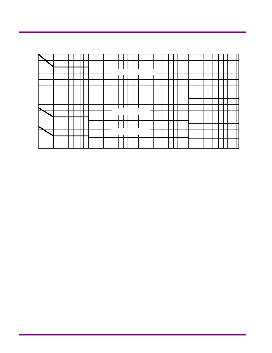
Vin ( VDC )
10uS
320
300
280
260
240
220
200
180
160
140
100uS
1mS
10mS
100mS
120
100
80
60
40
0
48VDC Input Models
24VDC Input Models
110VDC Input Models
Input Voltage Transient Rating
MIW2100 Series
4
MINMAX
REV:0 2005/04
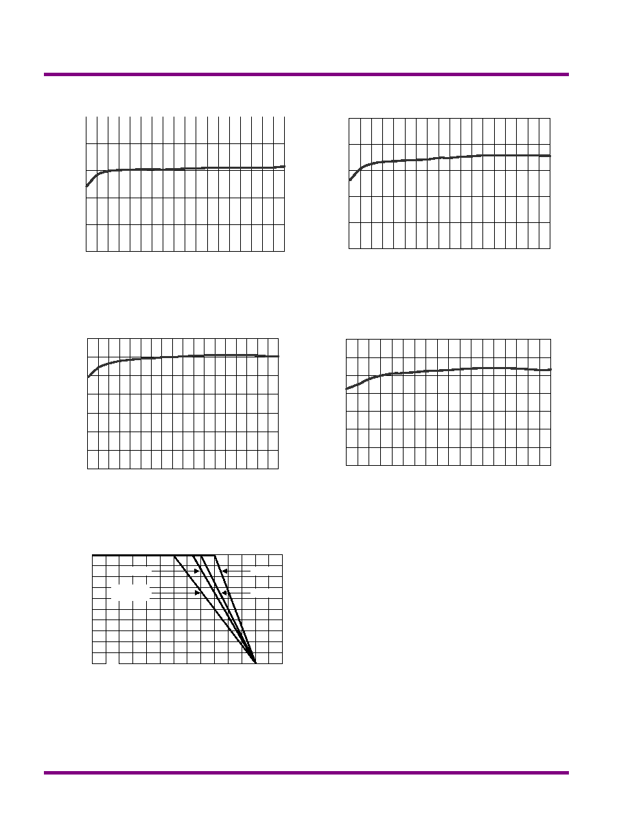
Derating Curve
]
Ambient Temperature
Output Power (%)
0
20
40
60
80
100
-40
50
60
80
100
110
90
70
400LFM
200LFM
100LFM
Natural
convection
Efficiency vs Output Load ( Dual Output )
Efficiency vs Output Load ( Single Output )
Load Current (%)
100
60
40
20
10
80
30
40
50
60
70
80
90
100
Efficiency (%)
20
30
40
50
60
70
80
90
Efficiency (%)
Load Current (%)
100
60
40
20
10
80
Efficiency vs Input Voltage ( Dual Output )
Efficiency vs Input Voltage ( Single Output )
50
60
70
80
90
100
Input Voltage (V)
Nom
Low
High
Efficiency (%)
50
60
70
80
90
100
Input Voltage (V)
Nom
Low
High
Efficiency (%)
MIW2100 Series
REV:0 2005/04
MINMAX
5
Test Configurations
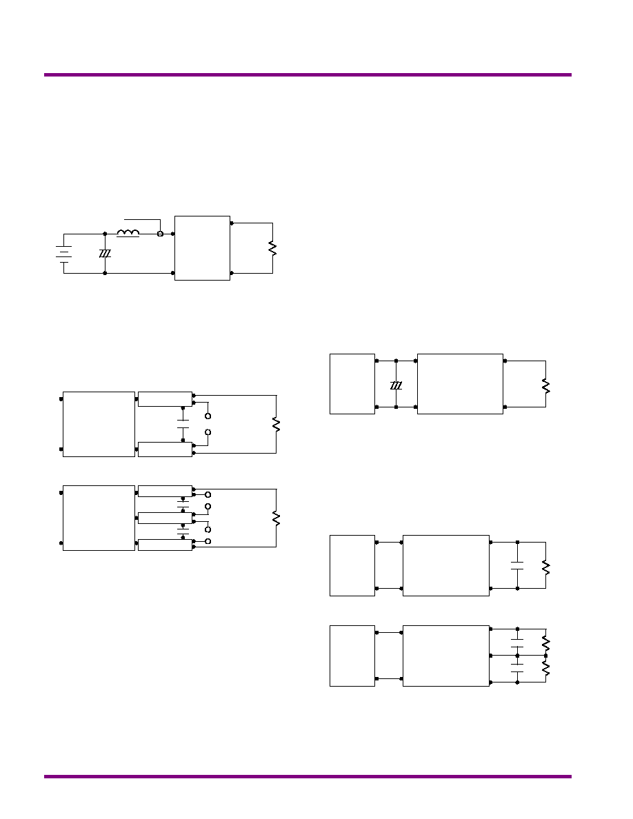
Input Reflected-Ripple Current Test Setup
Input reflected-ripple current is measured with a inductor
Lin (4.7uH) and Cin (220uF, ESR < 1.0[ at 100 kHz) to
simulated source impedance.
Capacitor Cin, offsets possible battery impedance.
Current ripple is measured at the input terminals of the
module, measurement bandwidth is 0-500KHz.
Peak-to-Peak Output Noise Measurement Test
Use a Cout 0.47uF ceramic capacitor.
Scope measurement should be made by using a BNC
socket, measurement bandwidth is 0-20 MHz. Position the
load between 50 mm and 75 mm from the DC/DC Converter.
Design & Feature Considerations
Maximum Capacitive Load
The MIW2100 series has limitation of maximum connected
capacitance on the output.
The power module may operate in current limiting mode
during start-up, affecting the ramp-up and the startup time.
Connect capacitors at the point of load for best
performance.
The maximum capacitance can be found in the data sheet.
Overcurrent Protection
To provide protection in a fault (output overload) condition,
the unit is equipped with internal current limiting circuitry and
can endure current limiting for an unlimited duration. At the
point of current-limit inception, the unit shifts from voltage
control to current control. The unit operates normally once the
output current is brought back into its specified range.
Input Source Impedance
The power module should be connected to a low
ac-impedance input source. Highly inductive source
impedances can affect the stability of the power module.
In applications where power is supplied over long lines and
output loading is high, it may be necessary to use a capacitor
on the input to insure startup.
By using a good quality low Equivalent Series Resistance
(ESR < 1.0[ at 100 kHz) capacitor of a 4.7uF for the 24V
input devices and a 2.2uF for the 48V devices, capacitor
mounted close to the power module helps ensure stability of
the unit.
Output Ripple Reduction
A good quality low ESR capacitor placed as close as
practicable across the load will give the best ripple and noise
performance.
To reduce output ripple, it is recommended that 3.3uF
capacitors are used on output.
MIW2100 Series
6
MINMAX
REV:0 2005/04
+Out
-Out
+Vin
-Vin
DC / DC
Converter
Load
Battery
+
Lin
+
Cin
To Oscilloscope
Current
Probe
+Out
-Out
+Vin
-Vin
Dual Output
DC / DC
Converter
Resistive
Load
Scope
Copper Strip
Cout
Com.
Scope
Cout
+Out
-Out
+Vin
-Vin
Single Output
DC / DC
Converter
Resistive
Load
Scope
Copper Strip
Cout
+
+Out
-Out
+Vin
-Vin
DC / DC
Converter
Load
DC Power
Source
+
-
Cin
+Out
-Out
+Vin
-Vin
Load
DC Power
Source
+
-
Cout
Com.
Dual Output
DC / DC
Converter
+Out
-Out
+Vin
-Vin
Load
DC Power
Source
+
-
Cout
Single Output
DC / DC
Converter
Thermal Considerations
Many conditions affect the thermal performance of the
power module, such as orientation, airflow over the module,
and board spacing. To avoid exceeding the maximum
temperature rating of the components inside the power
module, the case temperature must be kept below 90�C.
The derating curves were determined from measurements
obtained in an experimental apparatus.
Safety according to EN 60950 / UL 1950
Insulation between adjacent primary circuits or between
primary & secondary circuits:
Operational-,Basic- and Supplementary insulation for
working voltages up to 420 VDC /300 VAC.
Reinforced insulation for working voltages up to 210 VDC /
150 VAC.
Insulation between adjacent secondary circuits:
Operatonal-,Basic- Supplementary and Reinforced
insulation for working voltages up to 420 VDC /300 VAC.
Electromagnetic emission EN 55022 < B
Conducted and radiated emissions
MIW214X-types EN 55022 < A ; with external coupling
capacitor Cio=1 nF < B
MIW2100 Series
REV:0 2005/04
MINMAX
7
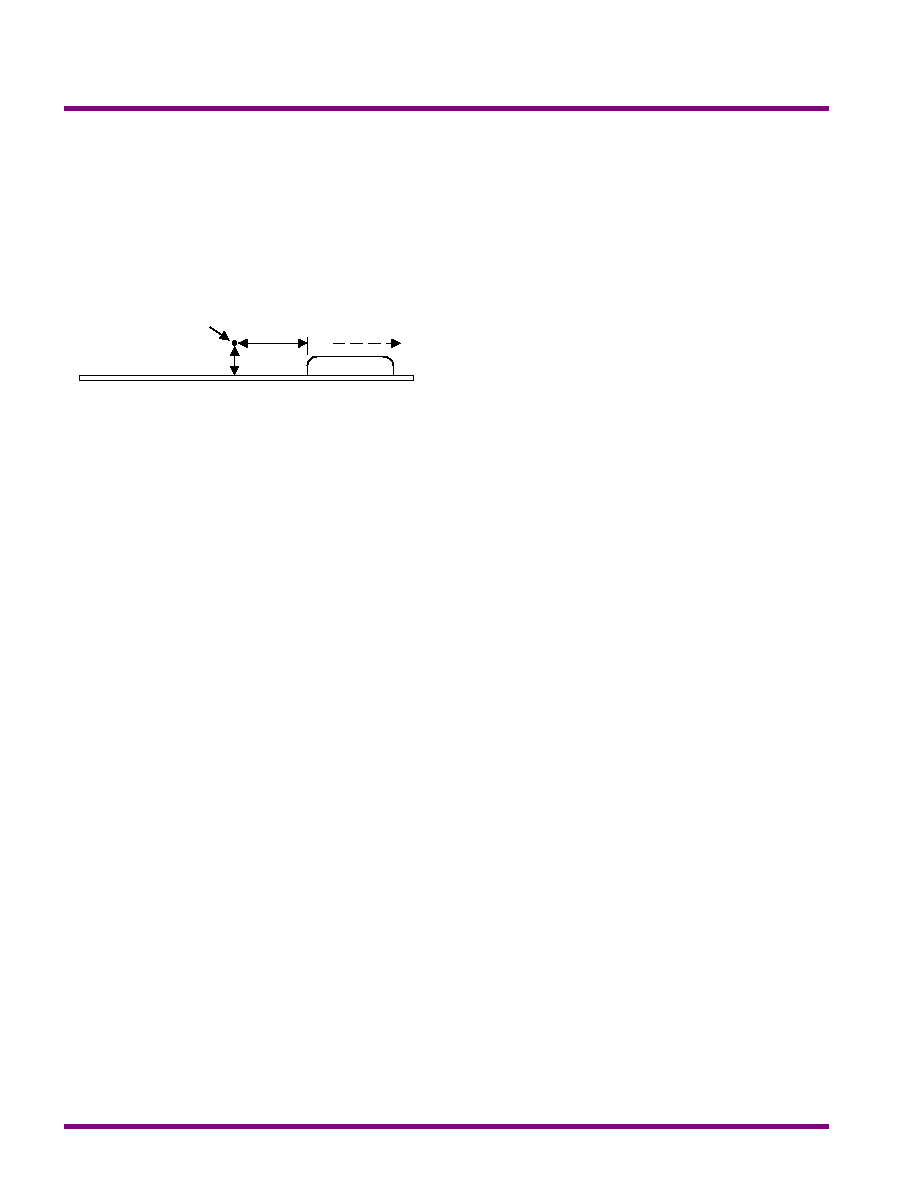
DUT
Position of air velocity
probe and thermocouple
50mm / 2in
Air Flow
15mm / 0.6in
The MIW2100 converter is encapsulated in a low thermal resistance molding compound that has excellent resistance/electrical
characteristics over a wide temperature range or in high humidity environments.
The encapsulant and unit case are both rated to UL 94V-0 flammability specifications.
Leads are tin plated for improved solderability.
UL94V-0
:
Flammability
-Vin
-Vin
24
-Vin
-Vin
23
16.2g
:
Weight
+Vout
No Pin
15
-Vout
+Vout
13
Non-Conductive Black Plastic
:
Case Material
No Pin
-Vout
12
Common
No Pin
11
1.25*0.8*0.40 inches
+Vin
+Vin
1
31.8*20.3*10.2 mm
:
Case Size
Dual Output
Single Output
Pin
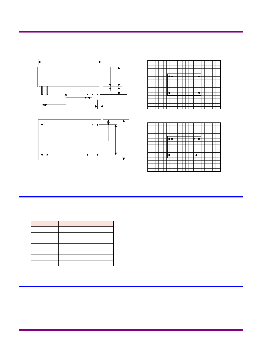
Physical Characteristics
Pin Connections
{0.002
{0.05
Pin
X.XXX{0.005
X.XX{0.13
X.XX{0.01
X.X{0.25
Inches
Millimeters
Tolerance
Dual Output
Single Output
31.8[1.25]
0.6[0.024]
2.54[0.100]
2.0[0.08]
10.5[0.41]
3.9[0.15]
15.2[0.06]
20.3[0.80]
1
24
13
Bottom
Side
2.54[0.10]
23
15
11 12
0.20[0.008]
Connecting Pin Patterns
Top View ( 2.54 mm / 0.1 inch grids )
Mechanical Dimensions
MIW2100 Series
8
MINMAX
REV:0 2005/04