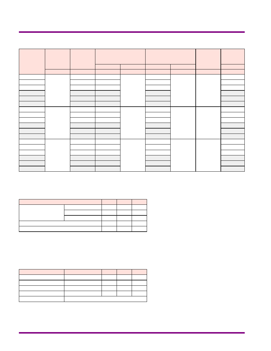
Dual Output
+Vo
Bipolar
Push-Pull
Inverter
+Vin
-Vin
Com.
-Vo
LC
Filter
Single Output
+Vo
Bipolar
Push-Pull
Inverter
+Vin
-Vin
-Vo
LC
Filter
Block Diagram
Low Noise
I/O Isolation
8000
VDC
Low Cost
$
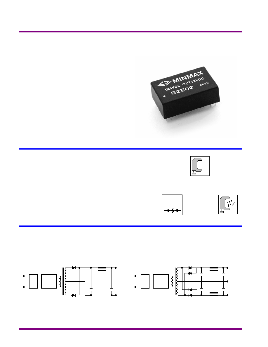
Minmax's S2E00 Model 1.5W DC/DC's are specially
designed to provide 30mA output ripple, continuous short
circuit in a low-profile 24-pin DIP package.
The series consists of 18 models with input voltages of
5V, 12V and 15VDC which offers regulated output voltages of
5V, 12V, 15V, {5V, {12V and {15VDC.
The -40] to +85] operating temperature range makes
it ideal for data communication equipments, mobile battery
driven equipments,distributed power systems,
telecommunication equipments, mixed analog/digital
subsystems, automatic test instrumentation and industrial
robot systems.
Meets EN60950 and EN60601-1
Low Leakage Current
Low Isolation Capacitance
Temperature Performance -40] to +85]
Output 5, 12, 15, {5, {12 and {15VDC
Input 5, 12 and 15VDC
30mV P-P Ripple and Noise
MTBF > 2,000,000 Hours
8000VDC Isolation
Low Cost
Key Features
1.5W, Ultra-High Isolation DIP, Single & Dual Output DC/DC Converters
S2E00 Series
REV:0 2005/04
MINMAX
1
75
133
{50
{15
S2E18
75
133
{63
{12
S2E17
75
133
{150
{5
S2E16
75
133
100
15
S2E15
75
133
125
12
S2E14
75
20
30
133
0
300
5
15
(13.5 ~ 16.5)
S2E13
75
167
{50
{15
S2E12
75
167
{63
{12
S2E11
75
167
{150
{5
S2E10
75
167
100
15
S2E09
75
167
125
12
S2E08
75
25
30
167
0
300
5
12
(10.8 ~ 13.2)
S2E07
75
400
{50
{15
S2E06
75
400
{63
{12
S2E05
75
400
{150
{5
S2E04
75
400
100
15
S2E03
75
400
125
12
S2E02
75
30
50
400
0
300
5
5
(4.5 ~ 5.5)
S2E01
% (Typ.)
mA (Typ.)
mA (Typ.)
mA (Typ.)
mA
mA
VDC
VDC
@Max. Load
@No Load
@Max. Load
Min.
Max.
Efficiency
Reflected
Ripple
Current
Input Current
Output Current
Output
Voltage
Input
Voltage
Model
Number
Model Selection Guide
Free-Air Convection
Cooling
%
95
---
Humidity
]
+125
-55
Storage Temperature
]
+95
-40
Case
Operating Temperature
]
+85
-40
Ambient
Operating Temperature
Unit
Max.
Min.
Conditions
Parameter
Environmental Specifications
Exceeding the absolute maximum ratings of the unit could cause damage.
These are not continuous operating ratings.
mW
1,000
---
Internal Power Dissipation
]
260
---
Lead Temperature (1.5mm from case for 10 Sec.)
VDC
21
-0.7
15VDC Input Models
VDC
17
-0.7
12VDC Input Models
VDC
7
-0.7
5VDC Input Models
Input Surge Voltage
( 1000 mS )
Unit
Max.
Min.
Parameter
Notes :
1. Specifications typical at Ta=+25], resistive load,
nominal input voltage, rated output current unless
otherwise noted.
2. Ripple & Noise measurement bandwidth is 0-20
MHz.
3. All DC/DC converters should be externally fused at
the front end for protection.
4. Operation under no-load conditions will not
damage these modules; however, they may not
meet all specifications listed.
5. Other input and output voltage may be available,
please contact factory.
6. Specifications subject to change without notice.
Absolute Maximum Ratings
S2E00 Series
2
MINMAX
REV:0 2005/04
KHz
100
---
50
Switching Frequency
pF
15
10
---
100KHz,1V
Isolation Capacitance
G[
---
---
10
500VDC
Isolation Resistance
uA
2
---
---
240VAC, 60Hz
Leakage Current
VDC
---
---
8800
Flash Tested for 1 Second
Isolation Voltage Test
VDC
---
---
8000
60 Seconds
Isolation Voltage Rated
Unit
Max.
Typ.
Min.
Conditions
Parameter
General Specifications
Continuous
Output Short Circuit
%/]
{0.02
{0.01
---
Temperature Coefficient
%
---
---
120
Over Load
mV rms
10
---
---
Ripple & Noise (20MHz)
mV P-P
50
---
---
Over Line, Load & Temp.
Ripple & Noise (20MHz)
mV P-P
40
30
---
Ripple & Noise (20MHz)
%
{6.0
{4.0
---
Load Regulation(15,{15V Output)
%
{8.0
{6.0
---
Load Regulation(12,{12V Output)
%
{12
{8.0
---
Load Regulation({5V Output)
%
{10
{7.0
---
Io=20% to 100%
Load Regulation(5V Output)
%
{1.5
{1.2
---
For Vin Change of 1%
Line Regulation
%
{2.0
{0.5
---
Dual Output, Balanced Loads
Output Voltage Balance
%
{4.0
{2.0
---
Output Voltage Accuracy
Unit
Max.
Typ.
Min.
Conditions
Parameter
Output Specifications
Pi Filter
Input Filter
mW
1000
---
---
Short Circuit Input Power
A
0.5
---
---
All Models
Reverse Polarity Input Current
16.5
15
13.5
15V Input Models
13.2
12
10.8
12V Input Models
VDC
5.5
5
4.5
5V Input Models
Input Voltage Range
Unit
Max.
Typ.
Min.
Model
Parameter
Input Specifications
K Hours
---
---
2000
MIL-HDBK-217F @ 25], Ground Benign
MTBF
# For each output
uF
220
220
220
470
470
470
Maximum Capacitive Load
Unit
{15V #
{12V #
{5V #
15V
12V
5V
Models by Vout
Capacitive Load
250mA Slow - Blow Type
250mA Slow - Blow Type
1000mA Slow - Blow Type
15V Input Models
12V Input Models
5V Input Models
Input Fuse Selection Guide
S2E00 Series
REV:0 2005/04
MINMAX
3
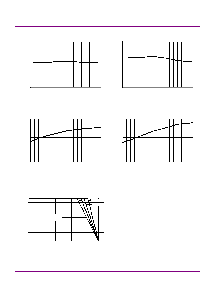
Derating Curve
]
Ambient Temperature
Output Power (%)
0
20
40
60
80
100
-40
50
60
80
100
110
90
70
400LFM
200LFM
100LFM
Natural
convection
Efficiency vs Output Load ( Dual Output )
Efficiency vs Output Load ( Single Output )
20
30
40
50
60
70
80
90
Load Current (%)
Efficiency (%)
100
60
40
20
10
80
20
30
40
50
60
70
80
90
Load Current (%)
Efficiency (%)
100
60
40
20
10
80
Efficiency vs Input Voltage ( Dual Output )
Efficiency vs Input Voltage ( Single Output )
50
60
70
80
90
100
Efficiency (%)
Input Voltage (V)
Nom
Low
High
50
60
70
80
90
100
Efficiency (%)
Input Voltage (V)
Nom
Low
High
S2E00 Series
4
MINMAX
REV:0 2005/04
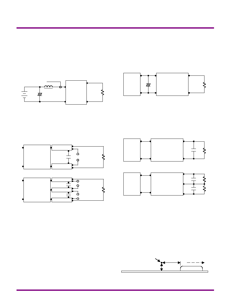
Test Configurations
Input Reflected-Ripple Current Test Setup
Input reflected-ripple current is measured with a inductor
Lin (4.7uH) and Cin (220uF, ESR < 1.0[ at 100 KHz) to
simulate source impedance.
Capacitor Cin, offsets possible battery impedance.
Current ripple is measured at the input terminals of the
module, measurement bandwidth is 0-500 KHz.
Peak-to-Peak Output Noise Measurement Test
Use a Cout 0.33uF ceramic capacitor.
Scope measurement should be made by using a BNC
socket, measurement bandwidth is 0-20 MHz. Position the
load between 50 mm and 75 mm from the DC/DC Converter.
Design & Feature Considerations
Maximum Capacitive Load
The S2E00 series has limitation of maximum connected
capacitance at the output.
The power module may be operated in current limiting
mode during start-up, affecting the ramp-up and the startup
time.
For optimum performance we recommend 220uF
maximum capacitive load
for each dual outputs and 470
u
F
capacitive load
for single outputs.
The maximum capacitance can be found in the data sheet.
Input Source Impedance
The power module should be connected to a low
ac-impedance input source. Highly inductive source
impedances can affect the stability of the power module.
In applications where power is supplied over long lines and
output loading is high, it may be necessary to use a capacitor
at the input to ensure startup.
Capacitor mounted close to the power module helps
ensure stability of the unit, it is recommended to use a good
quality low Equivalent Series Resistance (ESR < 1.0[ at 100
KHz) capacitor of a 2.2uF for the 5V input devices, a 1.0uF for
the 12V input devices and a 0.47uF for the 15V devices.
Output Ripple Reduction
A good quality low ESR 1.5uF capacitor connected as
colse as possible to the load is recommended.
Thermal Considerations
Many conditions affect the thermal performance of the
power module, such as orientation, airflow over the module
and board spacing. To avoid exceeding the maximum
temperature rating of the components inside the power
module, the case temperature must be kept below 95�C.
The derating curves are determined from measurements
obtained in an experimental apparatus.
S2E00 Series
REV:0 2005/04
MINMAX
5
+Out
-Out
+Vin
-Vin
DC / DC
Converter
Load
Battery
+
Lin
+
Cin
To Oscilloscope
Current
Probe
+Out
-Out
+Vin
-Vin
Dual Output
DC / DC
Converter
Resistive
Load
Scope
Copper Strip
Cout
Com.
Scope
Cout
+Out
-Out
+Vin
-Vin
Single Output
DC / DC
Converter
Resistive
Load
Scope
Copper Strip
Cout
+
+Out
-Out
+Vin
-Vin
DC / DC
Converter
Load
DC Power
Source
+
-
Cin
+Out
-Out
+Vin
-Vin
Load
DC Power
Source
+
-
Cout
Com.
Dual Output
DC / DC
Converter
+Out
-Out
+Vin
-Vin
Load
DC Power
Source
+
-
Cout
Single Output
DC / DC
Converter
DUT
Position of air velocity
probe and thermocouple
50mm / 2in
Air Flow
15mm / 0.6in