 | –≠–ª–µ–∫—Ç—Ä–æ–Ω–Ω—ã–π –∫–æ–º–ø–æ–Ω–µ–Ω—Ç: MIPS324KP | –°–∫–∞—á–∞—Ç—å:  PDF PDF  ZIP ZIP |
MIPS32 4KpTM Processor Core Datasheet
March 6, 2002
MIPS32 4KpTM Processor Core Datasheet, Revision 01.07
Copyright © 1999-2002 MIPS Technologies Inc. All right reserved.
The MIPS32TM 4KpTM core from MIPSÆ Technologies is a member of the MIPS32 4KTM processor core family. It is a
high-performance, low-power, 32-bit MIPS RISC core designed for custom system-on-silicon applications. The core is
designed for semiconductor manufacturing companies, ASIC developers, and system OEMs who want to rapidly integrate
their own custom logic and peripherals with a high-performance RISC processor. It is highly portable across processes, and
can be easily integrated into full system-on-silicon designs, allowing developers to focus their attention on end-user
products. The 4Kp core is ideally positioned to support new products for emerging segments of the digital consumer,
network, systems, and information management markets, enabling new tailored solutions for embedded applications.
The 4Kp core implements the MIPS32 Architecture and contains all MIPS IITM instructions; special multiply-accumulate
(MAC), conditional move, prefetch, wait, and leading zero/one detect instructions; and the 32-bit privileged resource
architecture. The Memory Management Unit consists of a simple, fixed Block Address Translation (BAT) mechanism for
applications that do not require the full capabilities of a Translation Lookaside Buffer based MMU.
Instruction and data caches are fully configurable from 0 - 16 Kbytes in size. In addition, each cache can be organized as
direct-mapped or 2-way, 3-way, or 4-way set associative. Load and fetch cache misses only block until the critical word
becomes available. The pipeline resumes execution while the remaining words are being written to the cache. Both caches
are virtually indexed and physically tagged to allow them to be accessed in the same clock that the address is translated.
An optional Enhanced JTAG (EJTAG) block allows for single-stepping of the processor as well as instruction and data
virtual address breakpoints.
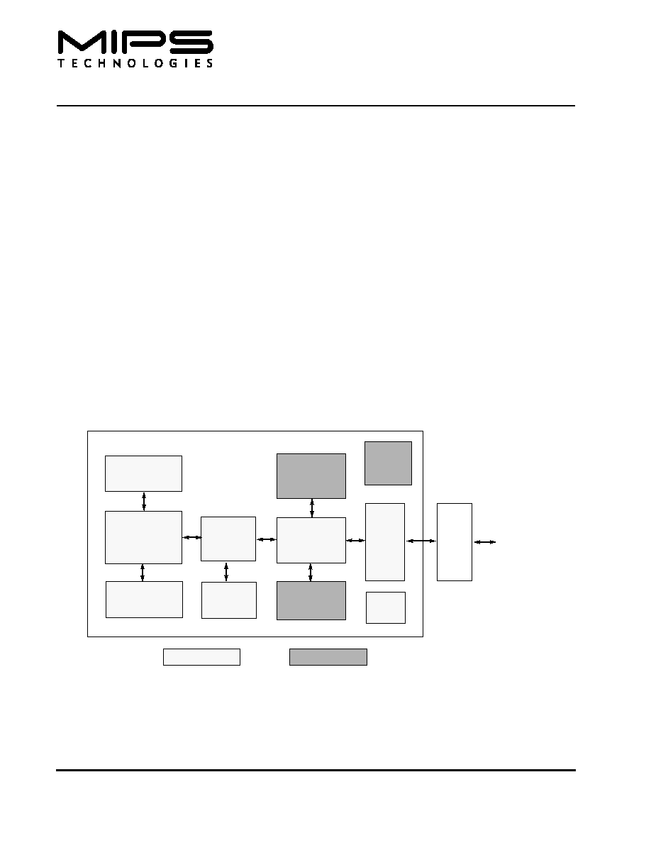
Figure 1
shows a block diagram of the 4Kp core. The core is divided into required and optional blocks as shown.
Figure 1 4Kp Core Block Diagram
Features
∑ 32-bit Address and Data Paths
Mul/Div Unit
Execution
Core
System
Coprocessor
MMU
BAT
EJTAG
Cache
Control
Instruction
Cache
Data
Cache
BIU
Thin I/F
On-Chip Bus(es)
Fixed/Required
Optional
Power
Mgmt.
Processor Core

2
MIPS32 4KpTM Processor Core Datasheet, Revision 01.07
Copyright © 1999-2002 MIPS Technologies Inc. All right reserved.
∑ MIPS32-Compatible Instruction Set
≠
All MIPS II Instructions
≠
Multiply-Accumulate and Multiply-Subtract
Instructions (MADD, MADDU, MSUB, MSUBU)
≠
Targeted Multiply Instruction (MUL)
≠
Zero/One Detect Instructions (CLZ, CLO)
≠
Wait Instruction (WAIT)
≠
Conditional Move Instructions (MOVZ, MOVN)
≠
Prefetch Instruction (PREF)
∑ Programmable Cache Sizes
≠
Individually configurable instruction and data caches
≠
Sizes from 0 - 16KB
≠
Direct Mapped, 2-, 3-, or 4-Way Set Associative
≠
Loads block only until critical word is available
≠
Write-through, no write-allocate
≠
16-byte cache line size, word sectored
≠
Virtually indexed, physically tagged
≠
Cache line locking support
≠
Non-blocking prefetches
∑ Scratchpad RAM Support
≠
Can optionally replace 1 way of the I- and/or D-cache
with a fast scratchpad RAM
≠
20 index address bits allow access of arrays up to 1MB
≠
Memory-mapped registers attached to the scratchpad
port can be used as a coprocessor interface
∑ R4000
Æ
-style Privileged Resource Architecture
≠
Count/Compare registers for real-time timer interrupts
≠
I and D watch registers for SW breakpoints
≠
Separate interrupt exception vector
∑ Memory Management Unit
≠
Simple Block Address Translation (BAT) mechanism
∑ Simple Bus Interface Unit (BIU)
≠
All I/Os fully registered
≠
Separate unidirectional 32-bit address and data buses
≠
Two 16-byte collapsing write buffers
∑ Multiply/Divide Unit
≠
32 clock latency on multiply
≠
34 clock latency on multiply-accumulate
≠
33-35 clock latency on divide (sign-dependent)
∑ Power Control
≠
Minimum frequency: 0 MHz
≠
Power-down mode (triggered by WAIT instruction)
≠
Support for software-controlled clock divider
∑ EJTAG Debug Support with single stepping, virtual
instruction and data address breakpoints
Architecture Overview
The 4Kp core contains both required and optional blocks.
Required blocks are the lightly shaded areas of the block
diagram in
Figure 1
and must be implemented to remain
MIPS-compliant. Optional blocks can be added to the 4Kp
core based on the needs of the implementation.
The required blocks are as follows:
∑ Execution Unit
∑ Multiply/Divide Unit (MDU)
∑ System Control Coprocessor (CP0)
∑ Memory Management Unit (MMU)
∑ Block Address Translation (BAT)
∑ Cache Controllers
∑ Bus Interface Unit (BIU)
∑ Power Management
Optional blocks include:
∑ Instruction Cache
∑ Data Cache
∑ Scratchpad RAM
∑ Enhanced JTAG (EJTAG) Controller
The section entitled
"4Kp Core Required Logic Blocks" on
page 3
discusses the required blocks. The section entitled
"4Kp Core Optional Logic Blocks" on page 10
discusses
the optional blocks.
Pipeline Flow
The 4Kp core implements a 5-stage pipeline with
performance similar to the R3000
Æ
pipeline. The pipeline
allows the processor to achieve high frequency while
minimizing device complexity, reducing both cost and
power consumption.
The 4Kp core pipeline consists of five stages:
∑ Instruction (I Stage)
∑ Execution (E Stage)
∑ Memory (M Stage)
∑ Align (A Stage)
∑ Writeback (W stage)
The 4Kp core implements a bypass mechanism that allows
the result of an operation to be forwarded directly to the
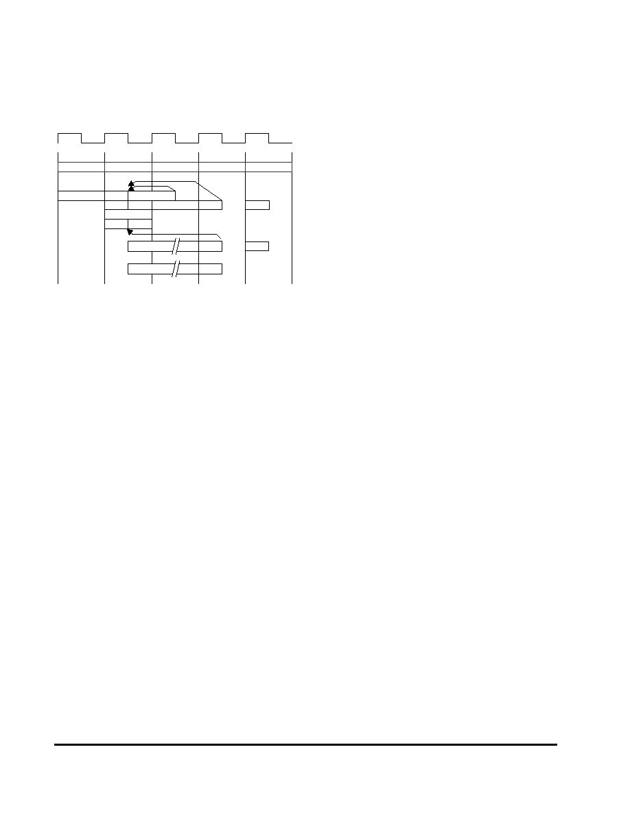
MIPS32 4KpTM Processor Core Datasheet, Revision 01.07
3
Copyright © 1999-2002 MIPS Technologies Inc. All right reserved.
instruction that needs it without having to write the result
to the register and then read it back.
Figure 2
shows a timing diagram of the 4Kp core pipeline.
Figure 2 4Kp Core Pipeline
I Stage: Instruction Fetch
During the Instruction fetch stage:
∑ An instruction is fetched from instruction cache.
E Stage: Execution
During the Execution stage:
∑ Operands are fetched from register file.
∑ The arithmetic logic unit (ALU) begins the arithmetic
or logical operation for register-to-register instructions.
∑ The ALU calculates the data virtual address for load
and store instructions.
∑ The ALU determines whether the branch condition is
true and calculates the virtual branch target address for
branch instructions.
∑ Instruction logic selects an instruction address.
∑ All multiply and divide operations begin in this stage.
M Stage: Memory Fetch
During the memory fetch stage:
∑ The arithmetic ALU operation completes.
∑ The data cache fetch and the data virtual-to-physical
address translation are performed for load and store
instructions.
∑ Data cache look-up is performed and a hit/miss
determination is made.
∑ A multiply operation stalls for 31 clocks in the M
stage.
∑ A multiply-accumulate operation stalls for 33 clocks in
the M stage.
∑ A divide operation stalls for 32-34 clocks in the M
stage.
A Stage: Align
During the Align stage:
∑ A separate aligner aligns load data to its word
boundary.
∑ A multiply/divide operation updates the HI/LO
registers.
∑ A MUL operation makes the result available for
writeback. The actual register writeback is performed
in the W stage.
W Stage: Writeback
∑ For register-to-register or load instructions, the
instruction result is written back to the register file
during the W stage.
4Kp Core Required Logic Blocks
The 4Kp core consists of the following required logic
blocks as shown in
Figure 1
. These logic blocks are defined
in the following subsections:
∑ Execution Unit
∑ Multiply/Divide Unit (MDU)
∑ System Control Coprocessor (CP0)
∑ Memory Management Unit (MMU)
∑ Block Address Translation (BAT)
∑ Cache Controller
∑ Bus Interface Control (BIU)
∑ Power Management
Execution Unit
The 4Kp core execution unit implements a load/store
architecture with single-cycle ALU operations (logical,
shift, add, subtract) and an autonomous multiply/divide
unit. The 4Kp core contains thirty-two 32-bit general-
purpose registers used for integer operations and address
calculation. The register file consists of two read ports and
one write port and is fully bypassed to minimize operation
latency in the pipeline.
I
E
M
A
W
I-A1
I-Cache
RegRd
I Dec
ALU Op
D-Cache
Align
RegW
D-AC
Bypass
Bypass
I-A2
MUL
RegW
mul, div
RegW
4
MIPS32 4KpTM Processor Core Datasheet, Revision 01.07
Copyright © 1999-2002 MIPS Technologies Inc. All right reserved.
The execution unit includes:
∑ 32-bit adder used for calculating the data address
∑ Address unit for calculating the next instruction
address
∑ Logic for branch determination and branch target
address calculation
∑ Load aligner
∑ Bypass multiplexers used to avoid stalls when
executing instructions streams where data producing
instructions are followed closely by consumers of their
results
∑ Leading Zero/One detect unit for implementing the
CLZ and CLO instructions
∑ Arithmetic Logic Unit (ALU) for performing bitwise
logical operations
∑ Shifter & Store Aligner
Multiply/Divide Unit (MDU)
The 4Kp core contains a multiply/divide unit (MDU) that
contains a separate pipeline for multiply and divide
operations. This pipeline operates in parallel with the
integer unit (IU) pipeline and does not stall when the IU
pipeline stalls. This allows the long-running MDU
operations to be partially masked by system stalls and/or
other integer unit instructions.
Multiply and divide operations are implemented with a
simple 1 bit per clock iterative algorithm. Any attempt to
issue a subsequent MDU instruction while a multiply/
divide is still active causes an MDU pipeline stall until the
operation is completed.
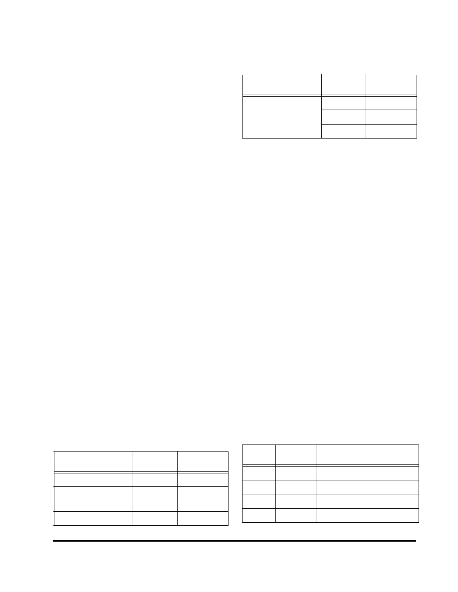
Table 1
lists the latency (number of cycles until a result is
available) for the 4Kp core multiply and divide
instructions. The latencies are listed in terms of pipeline
clocks.
The MIPS architecture defines that the results of a multiply
or divide operation be placed in the HI and LO registers.
Using the move-from-HI (MFHI) and move-from-LO
(MFLO) instructions, these values can be transferred to the
general-purpose register file.
As an enhancement to the MIPS II ISA, the 4Kp core
implements an additional multiply instruction, MUL,
which specifies that multiply results be placed in the
primary register file instead of the HI/LO register pair.
Two other instructions, multiply-add (MADD) and
multiply-subtract (MSUB), are used to perform the
multiply-accumulate and multiply-subtract operations,
respectively. The MADD instruction multiplies two
numbers and then adds the product to the current contents
of the HI and LO registers. Similarly, the MSUB
instruction multiplies two operands and then subtracts the
product from the HI and LO registers. The MADD and
MSUB operations are commonly used in DSP algorithms.
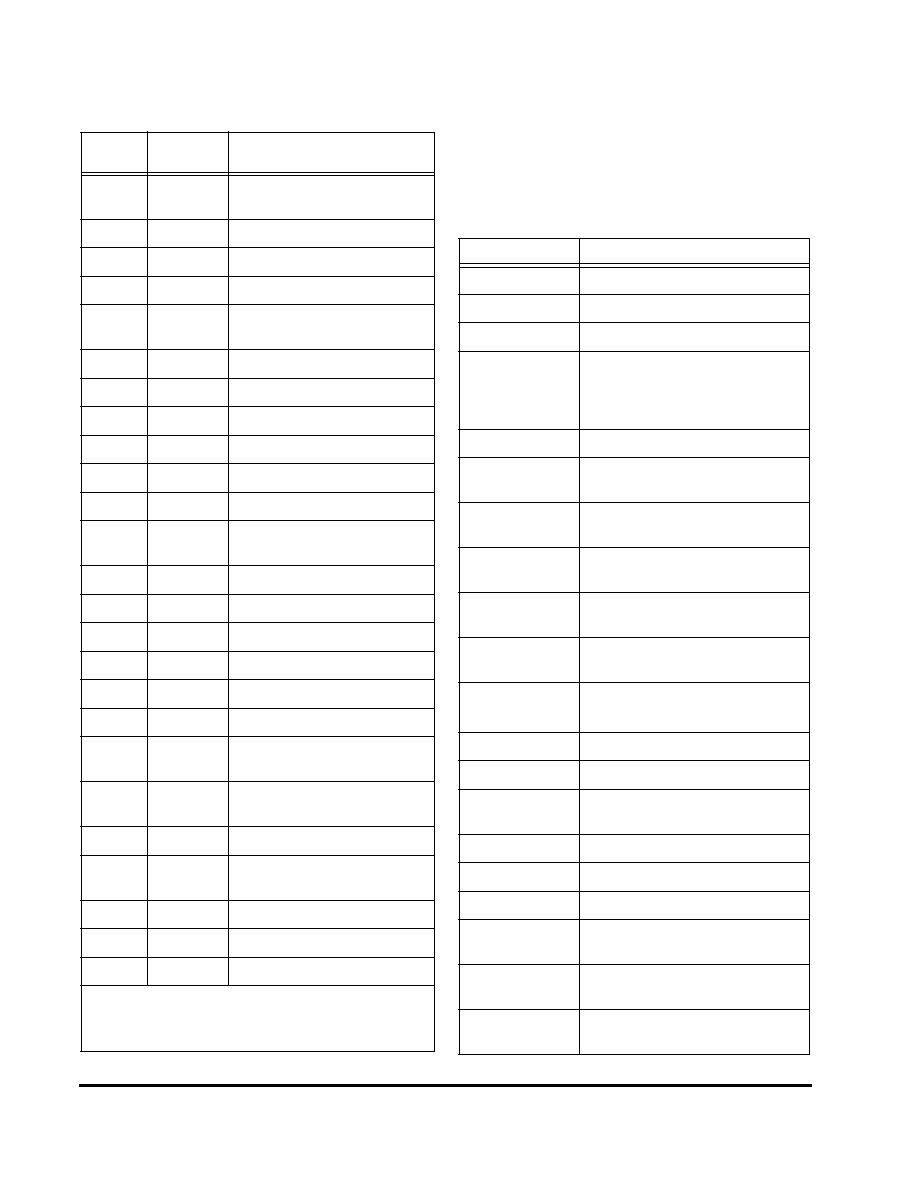
System Control Coprocessor (CP0)
In the MIPS architecture, CP0 is responsible for the virtual-
to-physical address translation and cache protocols, the
exception control system, the processor's diagnostics
capability, the operating modes (kernel, user, and debug),
and interrupts enabled or disabled. Configuration
information such as cache size and set associativity is
available by accessing the CP0 registers, listed in
Table 2
.
Table 1 4Kp Core Integer Multiply/Divide Unit
Operation Latencies
Opcode
Operand
Sign
Latency
MUL, MULT, MULTU
any
32
MADD, MADDU,
MSUB, MSUBU
any
34
DIVU
any
33
DIV
pos/pos
33
any/neg
34
neg/pos
35
Table 2 Coprocessor 0 Registers in Numerical Order
Register
Number
Register
Name
Function
0
Index
1
Reserved in the 4Kp core.
1
Random
1
Reserved in the 4Kp
core.
2
EntryLo0
1
Reserved in the 4Kp
core.
3
EntryLo1
1
Reserved in the 4Kp core.
Table 1 4Kp Core Integer Multiply/Divide Unit
Operation Latencies
Opcode
Operand
Sign
Latency
MIPS32 4KpTM Processor Core Datasheet, Revision 01.07
5
Copyright © 1999-2002 MIPS Technologies Inc. All right reserved.
Coprocessor 0 also contains the logic for identifying and
managing exceptions. Exceptions can be caused by a
variety of sources, including boundary cases in data,
external events, or program errors.
Table 3
shows the
exception types in order of priority.
4
Context
2
Pointer to page table entry in
memory.
5
PageMask
1
Reserved in the 4Kp core.
6
Wired
1
Reserved in the 4Kp core.
7
Reserved
Reserved.
8
BadVAddr
2
Reports the address for the most
recent address-related exception.
9
Count
2
Processor cycle count.
10
EntryHi
1
Reserved in the 4Kp core.
11
Compare
2
Timer interrupt control.
12
Status
2
Processor status and control.
13
Cause
2
Cause of last general exception.
14
EPC
2
Program counter at last exception.
15
PRId
Processor identification and
revision.
16
Config
Configuration register.
16
Config1
Configuration register 1.
17
LLAddr
Load linked address.
18
WatchLo
2
Low-order watchpoint address.
19
WatchHi
2
High-order watchpoint address.
20 - 22
Reserved
Reserved.
23
Debug
3
Debug control and exception
status.
24
DEPC
3
Program counter at last debug
exception.
25 - 27
Reserved
Reserved.
28
TagLo/
DataLo
Low-order portion of cache tag
interface.
29
Reserved
Reserved.
30
ErrorEPC
2
Program counter at last error.
31
DeSave
3
Debug handler scratchpad register.
1. Registers used in memory management.
2. Registers used in exception processing.
3. Registers used during debug.
Table 2 Coprocessor 0 Registers in Numerical Order
Register
Number
Register
Name
Function
Table 3 4Kp Core Exception Types
Exception
Description
Reset
Assertion of SI_ColdReset signal.
Soft Reset
Assertion of SI_Reset signal.
DSS
EJTAG Debug Single Step.
DINT
EJTAG Debug Interrupt. Caused by the
assertion of the external EJ_DINT
input, or by setting the EjtagBrk bit in
the ECR register.
NMI
Assertion of EB_NMI signal.
Machine Check
TLB write that conflicts with an
existing entry.
Interrupt
Assertion of unmasked hardware or
software interrupt signal.
Deferred Watch
Deferred Watch (unmasked by K|DM-
>!(K|DM) transition).
DIB
EJTAG debug hardware instruction
break matched.
WATCH
A reference to an address in one of the
watch registers (fetch).
AdEL
Fetch address alignment error.
Fetch reference to protected address.
TLBL
Fetch TLB miss.
IBE
Instruction fetch bus error.
DBp
EJTAG Breakpoint (execution of
SDBBP instruction).
Sys
Execution of SYSCALL instruction.
Bp
Execution of BREAK instruction.
RI
Execution of a Reserved Instruction.
CpU
Execution of a coprocessor instruction
for a coprocessor that is not enabled.
Ov
Execution of an arithmetic instruction
that overflowed.
Tr
Execution of a trap (when trap
condition is true).