 | –≠–ª–µ–∫—Ç—Ä–æ–Ω–Ω—ã–π –∫–æ–º–ø–æ–Ω–µ–Ω—Ç: MIPS645Kf | –°–∫–∞—á–∞—Ç—å:  PDF PDF  ZIP ZIP |
MIPS64TM 5KfTM Processor Core Datasheet
November 19, 2001
MIPS64TM 5KfTM Processor Core Datasheet, Revision 01.03
Copyright © 1999-2001 MIPS Technologies Inc. All right reserved.
The MIPS64TM 5KfTM processor core from MIPS Technologies is a synthesizable, highly-integrated 64-bit MIPSÆ RISC
microprocessor core designed for high-performance, low-power, low-cost embedded applications. To semiconductor
manufacturing companies and system OEMs who are building complex System-On-Chip ASIC devices, the 5Kf core offers
the long-awaited benefits of an easy-to-integrate, synthesizable core that provides 64-bit address and data paths along with
the 64-bit computing power of an R5000
Æ
-class processor. The 5Kf core is portable across processes, is highly
configurable, and is easily integrated into standard design flows, thereby reducing time to market and allowing designers
to focus their attention on end-user products. The 5Kf core is ideally positioned to support new products for emerging
segments of the digital consumer, network, and office automation markets where floating point performance is required.
The power-management features of the 5Kf core make it ideally suited for use in battery-powered applications.
The 5Kf core implements the MIPS64 Architecture. It contains special multiply-accumulate, conditional move, prefetch,
wait, leading zero/one detect instructions, and the 64-bit privileged resource architecture. The 5Kf core also features a high
performances IEEE 754 compliant Floating Point Unit (FPU). The FPU supports both single and double precision
instructions. It includes the multiply add instruction, which can issue every cycle, whereby both a multiply and an add
single precision operation can be performed in every cycle. The 5Kf core can dual issue a floating point arithmetic
instruction with a floating point load/store or integer instruction, whereby two instructions can be executed every cycle in
floating point applications. A coprocessor interface is also provided, which allows designers a way to easily extend their
architectures by addition of custom functionality, such as network, or graphics coprocessors.
The memory management unit contains a configurable 16, 32, or 48 dual-entry Joint TLB (JTLB) with variable page sizes,
a 4-entry Instruction micro TLB (ITLB), and a 4-entry Data micro TLB (DTLB). Using a TLB with the 5Kf core is optional.
The alternative is to use a far simpler Fixed Mapping Translation (FMT) scheme.
Optional instruction and data caches are fully configurable from 0 - 64 KBytes in size, with a maximum size of 16 KBytes/
way in a 4-way set associative implementation. In addition, each cache can be organized as direct-mapped, 2-way, 3-way,
or 4-way set associative. The 5Kf core supports an instruction scheduling mechanism that eliminates pipeline stalls on
cache misses, and a load scheduling slot is also supported.
To ease software debugging, the EJTAG debug solution in the 5Kf core includes instruction software breakpoints, a single-
step feature, and a dedicated Debug Mode. Optional hardware breakpoints include 4 instruction and 2 data breakpoints. An
optional Test Access Port (TAP) forms the interface to an external debug host and provides a dedicated communication
channel for debugging of an embedded system.
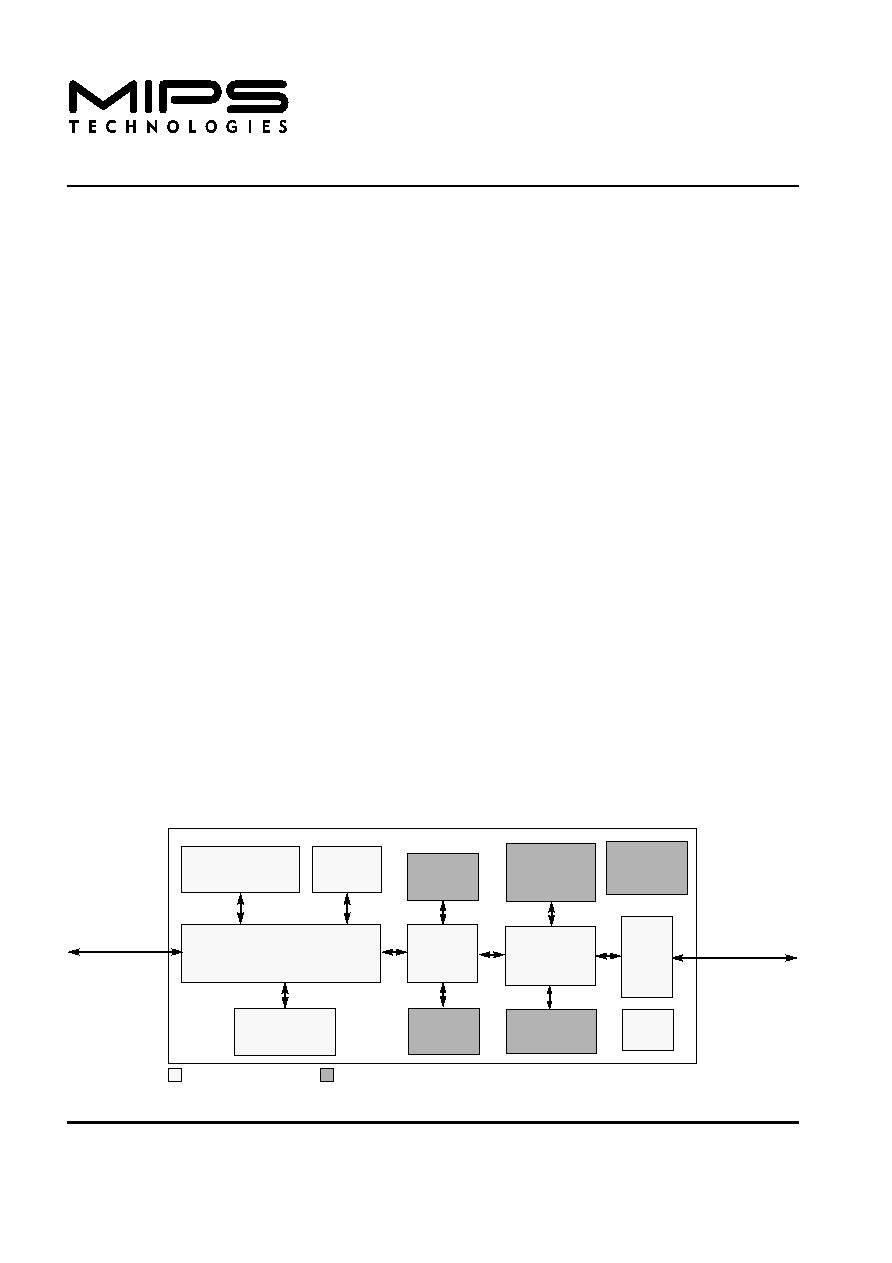
Figure 1
shows a block diagram of the 5Kf core. The core is divided into required and optional blocks as shown.
Figure 1 5Kf Core Block Diagram
Mul/Div
Execution Core
System
Coprocessor
MMU
TLB
EJTAG
Cache
Control
Instruction
Cache
Data
Cache
BIU
EC interface
Fixed/Required
Optional
Power
Mgmt.
5Kf Core
Breakpoints
TAP Ctrl
COP interface
FMT
Floating Point
Unit (FPU)
Unit
Dual issue capability

Features
2
MIPS64TM 5KfTM Processor Core Datasheet, Revision 01.03
Copyright © 1999-2001 MIPS Technologies Inc. All right reserved.
Features
∑ 64-bit Data and Address Path
(42-bit virtual and 36-bit physical address space)
∑ MIPS64 Compatible Instruction Set
≠
Based on MIPS V
TM
Instruction Set Architecture
≠
Multiply-Accumulate and Multiply-Subtract
Instructions (MADD, MADDU, MSUB, MSUBU)
≠
Targeted Multiply Instruction (MUL)
≠
Zero/One Detect Instructions (CLZ, CLO, DLCO,
DCLZ)
≠
Wait Instruction (WAIT) for low power control
≠
Conditional Move Instructions (MOVZ, MOVN)
≠
Prefetch Instructions (PREF, PREFX)
∑ Dual-issue Floating Point Unit / Coprocessor 1
≠
Fully pipelined IEEE 754 compliant floating point unit
with both single and double precision instructions
≠
Includes multiply add instruction
≠
Maximum issue rate of one multiply add single
(MADD.S) instruction every clock
≠
Maximum issue rate of one multiply add double
(MADD.D) instruction every other clock
≠
FPU executes independently of integer pipeline
≠
Fast flush-to-zero mode to optimize performance
∑ Dual-issue superscalar micro-architecture capable of
executing:
≠
1 integer and 1 arithmetic floating point instruction
≠
1 floating point arithmetic and 1 floating point load/
store instruction
∑ General Purpose Coprocessor Interface
≠
Supports all MIPS V instructions
≠
Supports COP2 coprocessors
≠
Utilizes high-performance features of the integer unit
≠
Dual-issue capability as for floating point instructions
∑ Multiply/Divide Unit
≠
Maximum issue rate of one 32x16 multiply per clock
≠
Maximum issue rate of one 32x32 multiply every other
clock
≠
Maximum issue rate of one 64x64 multiply every 9 clocks
≠
37 clock latency on 32/32 divides
≠
69 clock latency on 64/64 divide
≠
Early-in feature for divides allows results sooner for
smaller dividend values
∑ MIPS64 privileged resource architecture
≠
Count/Compare registers for real-time timer interrupts
≠
Instruction and Data watch registers for software
breakpoints
≠
Separate interrupt exception vector
≠
Supervisor Mode operation
≠
Performance Monitoring logic for analyzing application
speed
∑ Memory Management Unit
≠
16, 32, or 48 dual-entry JTLB with variable page sizes
or a simple Fixed Mapping Translation (FMT)
mechanism (optional)
≠
4-entry instruction micro TLB
≠
4-entry data micro TLB
≠
Support for 8-bit ASID
≠
Support for 4 KB - 16 MB page sizes
∑ Programmable Cache Sizes
≠
Individually configurable instruction and data caches
≠
Sizes from 0 - 16 KBytes/way (64 KBytes maximum)
≠
Direct Mapped, 2-, 3-, or 4-Way Set Associative
≠
Non-blocking loads
≠
32-byte cache line size, doubleword sectored
≠
Virtually indexed, physically tagged
≠
Support for locking cache lines
≠
Non-blocking prefetches
≠
Optional parity protection
∑ Simple Bus Interface Unit (BIU)
≠
All I/Os fully registered
≠
Separate, unidirectional 36-bit address and 64-bit data
buses
≠
32-byte write buffer (4 doublewords)
≠
1-line (32-byte) eviction buffer
∑ Power Control
≠
Minimum frequency: 0 MHz
≠
Power-down mode (triggered by WAIT instruction)
≠
Support for software controlled clock divider
≠
Sleep mode: During this mode the clocks are shut off.
Sleep mode is entered automatically from power-down
mode after all bus activity stops.
∑ EJTAG Debug Support
≠
Software Debug Breakpoint Instruction (SDBBP)
≠
Single-step feature
≠
Debug Mode
≠
Optional hardware breakpoints (4 instruction and 2 data
breakpoints)
≠
Optional Test Access Port (TAP) interface to debug
host, including fast data download/upload feature
∑ Testability for Production Test:
≠
Muxed-FF fullscan design with configurable number of
scan chains. ATPG test coverage can exceed 99%
(library and configuration dependent).
≠
Optional memory BIST, either through integrated
memory test (March C+ or IFA-13 algorithm) or by use
of industry standard memory BIST CAD tools.
Architectural Overview
MIPS64TM 5KfTM Processor Core Datasheet, Revision 01.03
3
Copyright © 1999-2001 MIPS Technologies Inc. All right reserved.
Architectural Overview
The 5Kf core contains both required and optional blocks.
Optional blocks can be added to the 5Kf core based on the
needs of the implementation. The required blocks are as
follows:
∑ Execution Unit
∑ Floating Point Unit (FPU)
∑ Multiply/Divide Unit (MDU)
∑ System Control Coprocessor (CP0)
∑ Memory Management Unit (MMU)
∑ Translation Lookaside Buffer (TLB) or
Fixed Mapping Translation (FMT)
∑ Cache Controllers
∑ Bus Interface Unit (BIU)
∑ Basic EJTAG debug features
∑ Power Management
Optional blocks include:
∑ Instruction Cache
∑ Data Cache
∑ EJTAG Debug Test Access Port (TAP)
∑ EJTAG Hardware Breakpoints
∑ Memory BIST module
The section entitled
"5Kf Core Required Logic Blocks" on
page 4
discusses the required blocks. The section entitled
"5Kf Core Optional Logic Blocks" on page 16
discusses
the optional blocks.
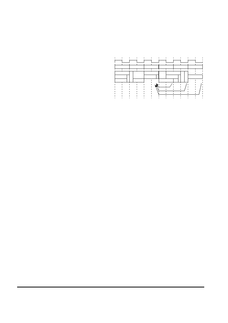
Pipeline Flow
The 5Kf core implements a high-performance 6-stage
pipeline:
∑ Instruction fetch (I stage)
∑ Dispatch (D stage)
∑ Register read (R stage)
∑ Execution (E stage)
∑ Memory access (M stage)
∑ Writeback (W stage)
The 5Kf core implements a bypass mechanism that allows
the result of an operation to be forwarded directly to the
instruction that needs it without having to write the result
to the register and then read it back.
Figure 2
shows a timing diagram of the 5Kf core pipeline.
Figure 2 5Kf Core Pipeline
I Stage: Instruction Fetch
During the Instruction Fetch stage:
∑ The Translation Lookaside Buffer (TLB) or the Fixed
Mapping Translation (FMT) performs the virtual-to-
physical address translation for instruction fetch
addresses.
∑ An instruction is fetched from instruction cache.
D Stage: Dispatch
During the Dispatch stage:
∑ Branch decode and prediction is performed.
∑ An instruction is dispatched to the coprocessor/integer
unit.
R Stage: Register Read
During the Register Read stage:
∑ The General Purpose Register (GPR) file is read.
∑ The instruction is decoded.
E Stage: Execution
During the Execution stage:
∑ The Arithmetic Logic Unit (ALU) computes the
arithmetic or logical operation for register-to-register
instructions.
∑ The ALU determines whether the branch condition is
true.
I
D
R
E
M
W
I$ Data
I$ Tag
T
ag Cmp.
ITLB
W
ay Select
Dispatch
Branch Tgt
GPR Read
Decode
GPR Write
Byp
Low
Addr
ALU/Addr
D$ Tag
DTLB
T
ag Cmp.
D$ Data
W
ay Select
Load Align
Bypass
Bypass
Bypass

Modes of Operation
4
MIPS64TM 5KfTM Processor Core Datasheet, Revision 01.03
Copyright © 1999-2001 MIPS Technologies Inc. All right reserved.
∑ All multiply and divide operations begin.
∑ The ALU calculates the full virtual address for load
and store instructions.
∑ The cache look-up starts for loads and stores.
M Stage: Memory Access
During the memory access stage:
∑ The Data Translation Lookaside Buffer (DTLB) or the
Fixed Mapping Translation (FMT) performs the
virtual-to-physical address translation for data load/
store addresses.
∑ The data cache lookup completes.
∑ Load data is aligned.
W Stage: Writeback
During the writeback stage:
∑ For register-to-register or load instructions, the
instruction result is written back to the register file.
Modes of Operation
The 5Kf core supports four modes of operation: User
Mode, Supervisor Mode, Kernel Mode, and Debug Mode.
User Mode is most often used for applications programs.
Kernel and Supervisor Modes are typically used for
handling exceptions and operating system functions,
including CP0 management and I/O device accesses.
Debug Mode is used for EJTAG software debugging and is
similar to Kernel Mode, but also allows programming of
debug resources and has special handling of exceptions and
other debug related issues.
The processor enters Kernel Mode both at reset and when
an exception is taken. While in Kernel Mode, software has
access to the entire address space as well as all CP0
registers. User Mode accesses are limited to a subset of the
virtual address space and can be inhibited from accessing
CP0 functions.
5Kf Core Required Logic Blocks
The 5Kf core consists of the following required logic
blocks as shown in
Figure 1
. These logic blocks are defined
in the following subsections:
∑ Execution Unit
∑ Floating Point Unit (FPU) / Coprocessor 1
∑ Multiply/Divide Unit (MDU)
∑ System Control Coprocessor (CP0)
∑ Cache Controllers
∑ Memory Management Unit (MMU)
∑ Translation Lookaside Buffer (TLB) or
Fixed Mapping Translation (FMT)
∑ Bus Interface Control (BIU)
∑ Basic EJTAG debug features
∑ Power Management
Execution Unit
The 5Kf core execution unit implements a load/store
architecture with single-cycle ALU operations (logical,
shift, add, subtract). The 5Kf core contains thirty-two 64-
bit general-purpose registers used for integer operations
and address calculation. The register file consists of two
read ports and two write ports and is fully bypassed to
minimize operation latency in the pipeline.
The execution unit includes:
∑ 64-bit adder used for calculating arithmetic results and
the data addresses
∑ Program counter the next instruction address
∑ Logic for branch determination and branch target
address calculation
∑ Load and store aligner
∑ Bypass multiplexers used to avoid stalls when
executing instructions streams where data producing
instructions are followed closely by consumers of their
results.
∑ Instruction buffer that eliminates penalties to the
pipeline when branches are predicted correctly, and
reduces the penalty to one pipeline bubble when a
branch is mispredicted.
∑ Zero/One detect unit for implementing the CLZ,
DCLZ, CLO, and DCLO instructions.
∑ Logic unit for performing bitwise logical operations
5Kf Core Required Logic Blocks
MIPS64TM 5KfTM Processor Core Datasheet, Revision 01.03
5
Copyright © 1999-2001 MIPS Technologies Inc. All right reserved.
Floating Point Unit (FPU) / Coprocessor 1
The 5Kf core Floating Point Unit (FPU) implements the
MIPS64 ISA (Instruction Set Architecture) for floating-
point computation. The implementation supports the
ANSI/IEEE Standard 754 (IEEE Standard for Binary
Floating-Point Arithmetic) for single and double precision
data formats. The FPU contains thirty-two 64-bit floating-
point registers used for floating point operations.
The performance is optimized for single precision formats.
Most instructions have a 1 cycle throughput and 4 cycle
latency. The FPU can dual issue arithmetic and load/store
instructions, whereby arithmetic operations can operate
continuously, while data is provided and retrieved.
The FPU implements the MIPS64 multiply-add (MADD)
and multiply-sub (MSUB) instructions with intermediate
rounding after the multiply function. The result is
guaranteed to be the same as executing a MUL and an ADD
instruction separately, but the instruction latency,
instruction fetch, dispatch bandwidth, and the total number
of register accesses are improved.
IEEE denormalized input operands and results are
supported by hardware for some instructions. IEEE
denormalized results are not supported by hardware in
general, but a fast flush-to-zero mode is provided to
optimize performance. The fast flush-to-zero mode is
enabled through the FCCR register, and use of this mode is
recommended for best performance when denormalized
results are generated.
The FPU has a separate pipeline for floating point
instruction execution. This pipeline operates in parallel
with the integer unit (IU) pipeline and does not stall when
the IU pipeline stalls. This allows long-running FPU
operations, such as divides or square root, to be partially
masked by system stalls and/or other integer unit
instructions. Arithmetic instructions are always dispatched
and completed in order, but loads and stores can complete
out of order. The exception model is `precise' at all times.
The FPU is also denoted coprocessor 1.
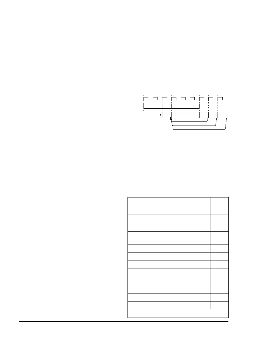
FPU Pipeline
The FPU implements a high-performance 7-stage pipeline:
∑ Decode, register read and unpack (FR stage)
∑ Multiply tree - double pumped for double (M1 stage)
∑ Multiply complete (M2 stage)
∑ Addition first step (A1 stage)
∑ Addition second and final step (A2 stage)
∑ Packing to IEEE format (FP stage)
∑ Register writeback (FW stage)
The FPU implements a bypass mechanism that allows the
result of an operation to be forwarded directly to the
instruction that needs it without having to write the result
to the FPU register and then read it back.
Figure 3
shows the FPU pipeline with dispatch from the
integer pipeline.
Figure 3 FPU Pipeline
FPU Instruction Latencies and Repeat Rates
Table 1
contains the floating point instruction latencies and
repeat rates for the common cases. In this table `Latency'
refers to the number of cycles necessary for the first
instruction to produce the result needed by the second
instruction. The `Repeat Rate' refers to the maximum rate
at which an instruction can be executed.
Table 1 5Kf Core FPU Latency and Repeat Rate
Opcode*
Latency
(cycles)
Repeat
Rate
(cycles)
ABS.[S,D], NEG.[S,D], ADD.[S,D],
SUB.[S,D], MUL.S, MADD.S,
MSUB.S, NMADD.S, NMSUB.S
4
1
MUL.D, MADD.D, MSUB.D,
NMADD.D, NMSUB.D
5
2
RECIP.S
13
10
RECIP.D
25
21
RSQRT.S
17
14
RSQRT.D
35
31
DIV.S, SQRT.S
17
14
DIV.D, SQRT.D
32
29
C.cond.[S,D] to FPU inst. / other inst.
1 / 2
1
CVT.D.S, CVT.[S,D].[W,L]
4
1
* Format: S = Single, D = Double, W = Word, L = Longword
I
D
R
FR
E
M1
M
M2
W
A1
A2
FP
FW
FPU Pipeline
Bypass
Bypass
Bypass
Integer Pipeline