 | –≠–ª–µ–∫—Ç—Ä–æ–Ω–Ω—ã–π –∫–æ–º–ø–æ–Ω–µ–Ω—Ç: JUPITER | –°–∫–∞—á–∞—Ç—å:  PDF PDF  ZIP ZIP |

The JUPITER circuit is designed for use in dual band and dual
mode mobile phones (CDMA/AMPS) and meets the requirements
for IS-95 when used with other chips from Mitel that form the
Planet chipset. JUPITER is an active filter incorporating circuits
for receiving both CDMA and FM (AMPS).
FEATURES
s
Low Power and Low Voltage Operation with a
Sleep Mode
s
Integrated CDMA and FM Filter with Wide
Dynamic Range
s
Low Inband Gain Ripple Performance and Good
I/Q Matching for the Filter
JUPITER
CDMA and FM (AMPS) I/Q Filter
Preliminary Information
DS4724 - 3.1 May 1998
ABSOLUTE MAXIMUM RATINGS
Supply voltage, V
CC MAX
Operating temperature, T
OP
(at pins)
Storage temperature, T
STG
(ambient)
Junction temperature
CMOS input logic high, V
IH
CMOS input logic low, V
IL
Maximum input voltage at all pins
ORDERING INFORMATION
JUPITER-1/KG/NP1S
2
0∑7V to 15∑3V
2
30
∞
C to170
∞
C
2
40
∞
C to 1150
∞
C
2
30
∞
C to 1125
∞
C
V
CC
1
0∑6V (Max.)
2
0∑6V (Min.)
2
0∑6V to V
CC MAX
1
0∑6V
ESD PROTECTION
All pins are protected against electrostatic discharge to both
supplies. At least 2kV protection is provided to MIL-STD-883D
Method 3015.7 (human body model).
Fig. 1 Pin connections - top view
NP28
Q_OC_TEST
Q_OC_TESTB
QIN
QINB
Q_OFFSET
Q_OFFSETB
V
TEST
RTUNE
ITUNE
QTUNE
QBAL
QOUT
QOUTB
V
CC
I_OC_TEST
I_OC_TESTB
IIN
IINB
I_OFFSET
I_OFFSETB
V
EE
MODE_CDMA
ENABLE
ENTEST
V
REF
IOUT
IOUTB
V
EE
2
1
2
3
4
5
6
7
8
9
10
11
12
13
14
28
27
26
25
24
23
22
21
20
19
18
17
16
15
JUPITER
Fig. 2 Simplified block diagram
GAIN
CONTROL
MODE
CONTROL
IIN
QIN
IOUT
QOUT
MODE
SELECT
INPUTS
TUNE
CONTROLS
FILTER
CONTROL
QBAL
V
GC
I CHANNEL
Q CHANNEL

JUPITER
2
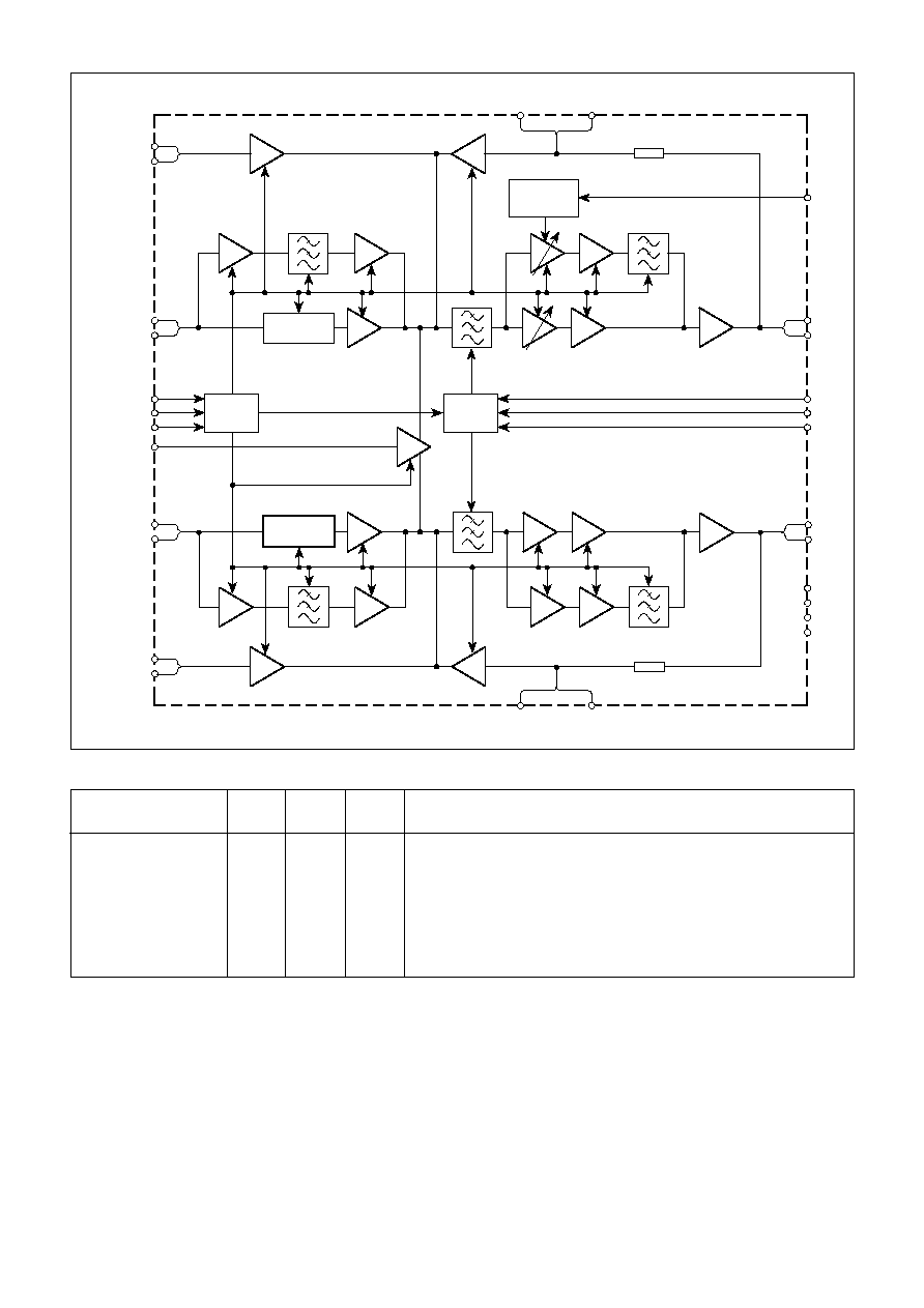
CIRCUIT DESCRIPTION
The block diagram of the JUPITER filter is shown in
Fig. 3. Two tunable active low-pass gyrator filters are designed
with balanced I/Q inputs and outputs.
CDMA MODE
In CDMA mode the filter (F1 on Fig. 3) is a 7th order 0.1dB
ripple continuously tunable elliptic type with the corner frequency
tuned to 690kHz for best stop band attenuation and minimal
phase error (in the overall system). Variable gain stages after the
filter provide the gain control capability. Overall, each of the
CDMA I/Q channels has 45dB nominal voltage gain with the Q
channel having
±
2dB gain adjustment range. Separate I/Q
frequency tuning functions are built into the device.
FM MODE
In FM mode the same filter is used; however, the biasing is
designed such that the current density in the transconductor cells
is reduced by a factor of 46, changing the filter's cutoff frequency
to 15kHz. The filter characteristic of the main channel filter
(gyrator filter) remains the same, i.e. a 0.1dB 7th order elliptic. In
FM mode additional 2nd order Sallen and Key 0.1dB ripple
Chebeyshev filters (F2) are included in the signal path prior to the
gyrators. These improve the out-of-band blocking of the overall
filter. Different amplifiers are used in FM mode to those used in
CDMA mode to enable optimization of the gain distribution in FM
mode for current consumption and dynamic range.
OPERATION
Signal inputs are DC coupled in both CDMA and FM modes.
The device modes are selected by CMOS compatible logic
signals as shown in Table 2. An external resistor should be
connected between RTUNE and ground to set internal currents;
a resistor with a tolerance of
6
5% and a temperature coefficient
of less than 100ppm is recommended. V
REF
(pin 18) should be
decoupled to V
CC
to give optimum supply rejection.
A test mode is provided for filter calibration. In this mode, a test
signal is applied to the V
TEST
input (pin 7) with ENTEST held high.
The test mode is designed to interface with the PLUTO baseband
processor, which can provide the test signal and I/QTUNE
voltages and calibrates the filters using an internal auto calibration
algorithm. The algorithm generates two test frequencies and
calibrates the filters to give the correct attenuation at the upper
frequency. The calibration is normally carried out in CDMA
mode: the FM filter performance is scaled accordingly.
Pins are provided for DC offset control for I and Q channels
(I_OFFSET, I_OFFSETB, Q_OFFSET and Q_OFFSETB). In
typical operation, the I_OFFSET/Q_OFFSET pins would be
controlled by a voltage derived from the baseband processor.
However, it is also possible to minimise the DC offset using
external components; this is primarily intended for test purposes.
These feedback components between IOUT/QOUT and
I_OFFSET/Q_OFFSET are shown in Fig. 4 but would not be
used in the normal application
In test mode, these offset controls are disabled and the offsets
are controlled using on-chip feedback. The loop filter for this
feedback uses external 10nF capacitors on pins I_OC_TEST/B
and Q_OC_TEST/B as shown in Fig. 4.
I/O
I
I
I
I
I
I
I
I
I
I
O
O
P
P
O
O
I
I
I
P
I
I
I
I
I
I
Description
Q channel offset control in test mode
Q channel offset control in test mode (balanced)
Q channel CDMA/FM input.
Q channel CDMA/FM input (balanced)
Q channel offset control
Q channel offset control (high gain mode)
Test mode signal input for tuning operation
Precision resistor for current definition (18k)
I filter tuning control
Q filter tuning control
Q channel gain adjust voltage, VGC
Q channel CDMA/FM output
Q channel CDMA/FM output (balanced)
Supply
Ground
I channel CDMA (balanced)
I channel CDMA
Reference voltage decouple
Mode control (see Table 2)
Mode control (see Table 2)
Mode control (see Table 2)
Ground (substrate)
I channel offset control (high gain mode)
I channel offset control
I channel CDMA (balanced)
I channel CDMA
I channel offset control in test mode (balanced)
I channel offset control in test mode
Name
Q_OC_TEST
Q_OC_TESTB
QIN
QINB
Q_OFFSET
Q_OFFSETB
V
TEST
RTUNE
ITUNE
QTUNE
QBAL
QOUT
QOUTB
V
CC
V
EE
2
IOUTB
IOUT
V
REF
ENTEST
ENABLE
MODE_CDMA
V
EE
I_OFFSETB
I_OFFSET
IINB
IIN
I_OC_TESTB
I_OC_TEST
Pin
1
2
3
4
5
6
7
8
9
10
11
12
13
14
15
16
17
18
19
20
21
22
23
24
25
26
27
28
Table 1 Pin descriptions
JUPITER
3
Fig. 3 Block diagram
All circuits powered down
Biasing and CDMA signal path on
Biasing and FM signal path on
Biasing, CDMA test and CDMA signal path on, excluding input amplifier
Biasing, FM test and FM signal path on, excluding input amplifier.
This is functionally the same as sleep mode but has higher I
CC
.
In sleep mode PLUTO applies a logic high to ENTEST
ENABLE
MODE_
CDMA
Sleep mode
CDMA mode
FM mode
CDMA filter testmode
FM filter test mode
Disallowed mode
0
1
1
1
1
0
X
1
0
1
0
X
1
0
0
1
1
0
Description
ENTEST
Comments
Table 2 Truth table for mode control lines
ENTEST
ENABLE
MODE_CDMA
QIN
QINB
MODE
CONTROL
ATTENUATOR
Q CHANNEL
±
2dB
50k
Q_OFFSET
Q_OFFSETB
gm
-0∑1
dB
gm
gm
gm
gm
gm
IIN
IINB
V
TEST
I_OFFSET
I_OFFSETB
gm
gm
-0∑1
dB
FILTER
CONTROL
QTUNE
RTUNE
ITUNE
QOUT
QOUTB
IOUT
IOUTB
QBAL
50k
gm
Q_OC_TESTB
Q_OC_TEST
I_OC_TESTB
I_OC_TEST
X1
X1
3
4
26
25
19
20
21
7
24
23
5
6
1
2
28
27
12
13
11
17
16
10
8
9
VEE2
VEE
VCC
VREF
ATTENUATOR
15
22
14
18
F3
F3
F1
F1
F2
F2
VGC

JUPITER
4
ELECTRICAL CHARACTERISTICS
The Electrical Characteristics are guaranteed over the following range of operating conditions unless otherwise
stated (see Fig. 4 for test circuit):
T
AMB
=
2
30
∞
C to
1
70
∞
C, V
CC
= 3V
1
0∑6V/
2
0∑3V
DC Characteristics
Characteristic
Conditions
General
Supply voltage, V
CC
Operating temperature, T
AMB
Supply Current, I
CC
Sleep mode
FM mode
CDMA mode
Turn off time, CDMA/FM
mode to Sleep mode
Mode Control Lines (CMOS)
Input logic high, V
IH
Input logic low, V
IL
Input high current I
IH
Input low current, I
IL
Tune/Gain Control Lines
DC level
Input impedances:
QBAL, ITUNE and QTUNE
I_OFFSET/B and Q_OFFSET/B
I/O DC Voltages
Inputs IIN/B and QIN/B
Outputs IOUT/B and QOUT/B
2∑7
2
30
2∑0
2
0∑1
2
20
2
20
0∑5
V
CC
2
0∑6
V
CC
2
1∑6
3∑6
1
70
0∑15
5∑2
11∑0
V
CC
1
0∑1
0∑5
20
20
2∑0
V
CC
2
0∑2
V
CC
2
1∑2
3∑0
3∑4
7∑3
100
200
500
V
CC
2
0∑4
V
CC
2
1∑4
QBAL = ITUNE = QTUNE <0∑5V
QBAL = ITUNE = QTUNE = 1∑2V
QBAL = ITUNE = QTUNE = 1∑2V
I
CC
reduced to 10% of active value
Referenced to on-chip ref. voltage (1∑2V)
V
∞
C
mA
mA
mA
µ
s
V
V
µ
A
µ
A
V
k
k
V
V
Units
Min.
Typ.
Max.
Value
%
All logic inputs

JUPITER
5
ELECTRICAL CHARACTERISTICS
FM Mode AC Characteristics
All parameters are defined as differential unless otherwise stated
Characteristic
Conditions
10
43
A
V
1
1∑5
8∑0
1
0∑75
6
0∑25
45
19∑5
5
1∑0
10
1∑4
4∑0
12
External load = 50k
//5pF
QBAL = 1∑2V
QBAL = 0∑5 to 2V
V
CC
=
6
150mV
Measured at I/Q output frequency = 10kHz
Measured at I/Q output frequency = 630kHz
Bandwidth = 10Hz to 5MHz. I and Q channels
Frequency = 2kHz
In-band frequency = 2kHz. All conditions
27
∞
C only
In-band frequency = 2kHz. All conditions
27
∞
C only
Unmodulated interferers
60kHz 75mVrms, 120kHz 7∑5mVrms
ITUNE = QTUNE = 1∑2V
Frequency = 100Hz to 12∑2kHz
Settling to within 5mV
Settling to within 5mV
Frequency = 2kHz
Frequency = 2kHz
MHz
dB
dB
dB/V
dB
dB
dB
dB
µ
Vrms
Vp-p
mVrms
mVrms
mVrms
mVrms
dBV
µ
Vrms
kHz
dB
dB
%
dBp-p
µ
s
deg
V/V
V/V
ms
ms
k
k
Units
Max.
Value
41
4∑0
10
0
30
1∑9
380
380
2
101
8∑8
16∑5
63
70
30
1∑0
10
4∑0
10
1∑0
Typ.
39
A
V
2
1∑5
6
2
2
0∑75
1∑5
266
266
14∑5
48
60
0∑6
8∑0
Min.
Maximum input frequency
Gain Characteristics
I voltage gain (A
V
) IIN/B to IOUT/B
Q voltage gain QIN/B to QOUT/B
Q channel gain adjust
Q channel gain control
Gain variation over temperature and
supply voltage
Differential output amplitude balance,
QOUT/QOUTB, IOUT/IOUTB
Power Supply Rejection
In-band
Out of band
Noise
Input referred
1dB Compression
Output 1dB compression
Out of band blocking signal causing 1dB
compression of in-band signal
Blocking signal at 60kHz
Blocking signal at 120kHz
Intermodulation
Input referred intermodulation product
Filter Characteristic (Note 1)
3dB pass band
Stop band attenuation 45kHz
Stop band attenuation 60kHz to 10MHz
I and Q bandwidth matching
In-band gain ripple
Group delay variation
Average phase balance, I and Q channels
Offset Loop Correction
Filter offset adjustment gain:
I_OFFSET/Q_OFFSET
I_OFFSET B/Q_OFFSETB
Amplifier offset settling time:
After power on
After CDMA to FM cycling
Input Impedances
QIN/QINB and IN/INB
Output Impedances
QOUT/QOUTB and IOUT/IOUTB
NOTE 1. Filter tuned in CDMA mode to
2
8dB at 720kHz
%