 | –≠–ª–µ–∫—Ç—Ä–æ–Ω–Ω—ã–π –∫–æ–º–ø–æ–Ω–µ–Ω—Ç: MH88422-2 | –°–∫–∞—á–∞—Ç—å:  PDF PDF  ZIP ZIP |

2-13
Features
∑
FAX and Modem interface (V29)
∑
Variants available with different line
impedances
∑
Provides reinforced barrier to international PTT
requirements
∑
Transformerless 2-4 Wire conversion.
∑
Integral Loop Switch
∑
Dial Pulse and DTMF operation
∑
Line state detection outputs
∑
Loop current/ringing outputs
∑
Single +5V operation, low on-hook power
(5mW)
∑
Full duplex data transmission
Applications
Interface to Central Office or PABX line for:
∑
Modem
∑
FAX
∑
Telemetry
Description
The Mitel MH88422 Data Access Arrangement
(D.A.A.) provides a complete interface between data
transmission equipment and a telephone line. All
functions are integrated into a single thick film hybrid
module which provides high voltage isolation, very
high reliability and optimum circuit design needing a
minimum of external components.
A number of variants are available to meet particular
country impedance requirements. The D.A.A. has
been designed to meet regulatory approvals
requirements in these countries.
Figure 1 - Functional Block Diagram
Opto-
Isolation
Logic Input
Buffer
Opto-
Isolation
Opto-
Isolation
Opto-
Isolation
Audio
Buffer
Audio
Buffer
Buffer
Transhybrid
loss
cancellation
circuit
Isolation Barrier
VDD
AGND
LC
VR
VX
RVLC
TIP
RING
User Connections
Network Connections
Input Buffer
&
TXIN
TF
RLS
Ring & Loop
Line Termination
DS5067
ISSUE 10
November 1998
Ordering Informations
MH88422-1/2/3 26 Pin DIL Package
MH88422BD-1 26 Pin DIL Package
0
∞
C to 70
∞
C
MH88422
Data Access Arrangement
Preliminary Information
MH88422
Preliminary Information
2-14
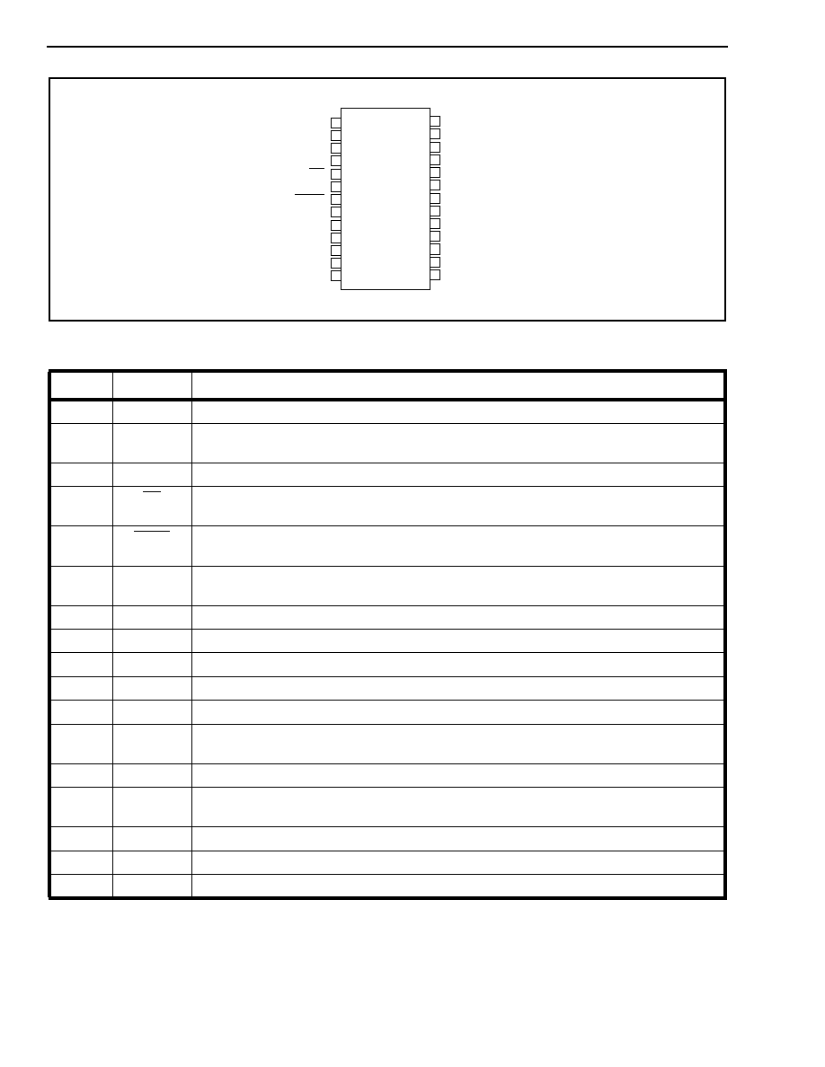
Figure 2 - Pin Connections
Notes:
1. Variant 1, 4 BD-1 - pins 10,12, & 21 are cropped short. Pin 23 is not fitted.
2. Variant 2 - pin 23 is cropped short. Pins 10, 12 & 21 are not fitted.
3. Variant 3 - pins 12 and 21 are cropped short. Pins 10 and 23 are not fitted.
Pin Description
Pin #
Name
Description
1
VDD
Positive Supply Voltage. +5V.
2, 4, 6,
8, 9
IC
Internal Connection. This pin is cropped short.
3
AGND
Analog Ground. 4-Wire Ground. Normally connected to System Ground.
5
LC
Loop Control (Input). A logic 0 activates internal circuitry which provides a line
termination across Tip and Ring. Used for seizing the line and dial pulsing.
7
RVLC
Ringing Voltage and Current Detect (Output). Indicates the status of loop current
and ringing voltage.
10, 12
IC/NP
Internal Connection or No Pin Fitted. This pin is either cropped short or not fitted,
depending on the variant. See Note 1
11
VX
Transmit (Output). Analog output to modem/fax chip set.
13
VR
Receive (Input). Analog input to modem/fax chip set.
14, 17
IC
Internal Connection. This pin is cropped short.
15, 19
NP
No Pin Fitted.
16
RING
Ring Lead. Connects to the "Ring" lead of a telephone line.
18
TXIN
Dummy Ringer Connection. Connects to the "Ring" lead of a telephone line through a
dummy ringer capacitor.
20
TF
Tip Feed. Connects externally to the RLS pin.
21, 23
IC/NP
Internal Connection or No Pin Fitted. This pin is either cropped short or not fitted,
depending on the variant. See Note 1
24
RLS
Ringing Loop Sense. Connects externally to the TF pin.
25
IC
Internal Connection. This pin is cropped short.
26
TIP
Tip Lead. Connects to the "Tip" lead of a telephone line.
VDD
IC
AGND
IC
LC
IC
RVLC
IC
IC/NP
VX
IC/NP
IC
1
2
3
4
5
6
7
8
9
10
11
12
15
16
17
18
26
25
24
23
22
21
20
19
13
14
VR
TIP
IC
RLS
IC/NP
IC
IC/NP
TF
NP
IC
RING
NP
TXIN
IC

Preliminary Information
MH88422
2-15
Functional Description
The device is a Data Access Arrangement (D.A.A.). It
is used to correctly terminate a 2-Wire analog loop. It
provides a signalling link and a 2-4 Wire line
interface between an analog loop and the
subscriber's data transmission equipment such as
Modems, Facsimiles (Fax's), Remote Metering and
Electronic Point of Sale equipment (EPOS).
Isolation Barrier
The device provides an isolation barrier implemented
by using optocouplers. This is a reinforced barrier for
an instantaneous power surge of up to 3kV r.m.s
., for
example a lightning strike. It also provides full
isolation for a continuous AC voltage level of up to
250V r.m.s.
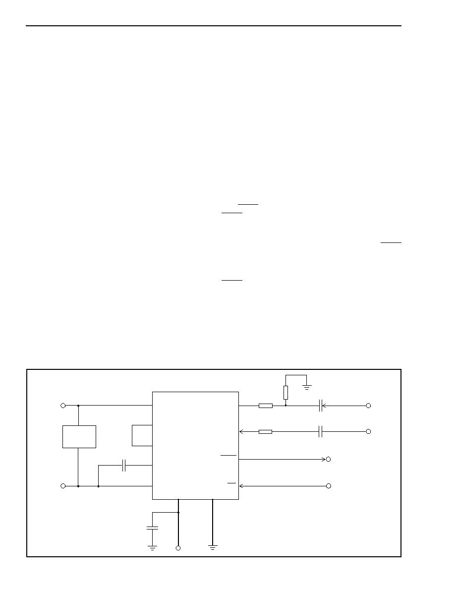
External Protection Circuit
Should the input voltage from the line exceed that
isolated by the optocoupler, an External Protection
Circuit assists in preventing damage to the device
and the subscriber equipment. See Figure 3.
Line Termination
When Loop Control (LC) is at a logic 0, a line
termination is applied across Tip and Ring. The
device can be considered off-hook and DC loop
current will flow. The line termination consists of both
a DC line termination and an AC input impedance.
When LC is at a logic 1, a Dummy Ringer is applied
across Tip and Ring. The device can be considered
on-hook and negligible DC current will flow. The
dummy ringer is an AC load, which represents a
telephone's mechanical ringer.
DC Line Termination
When LC is at a logic 0, an active termination is
applied across Tip and Ring, at which time it can be
considered to be in an off-hook state. This is used to
terminate an incoming call, seize the line for an
outgoing call, or if it is applied and disconnected at
the required rate, can be used to generate dial
pulses. This termination resembles approximately
300
resistance, which is loop current dependent.
Input Impedance
The MH88422 is available in a number of different
variants each of which has its own fixed Tip-Ring AC
input impedance (Zin). Each variant is identified by
the final digit in its part number, as listed below. Also
shown are the countries whose PTT requirements
match these impedances.
MH88422-1 Zin = 220
+ 820
// 120nF
Australia / South Africa / Spain
MH88422BD-1 Zin = 220
+ 820
// 115nF
German BABT ZV5
MH88422-2 Zin = 600
North America
MH88422-3
Zin = 370
+ 620
// 310nF
UK / New Zealand
Many of these countries now pass equipment
approved to CTR21. The MH88422 will not meet this
specification. See the MH88437 datasheet for a
CTR21 Product.
Dummy Ringer
This device supports a dummy ringer option which
can be configured by the inclusion of external
components. Further details relating to component
values and configuration can be obtained from
MSAN-154. For example, Figure 3 shows capacitor
C2 which if set to 1.8
µ
F would meet the New
Zealand dummy ringer requirements.
2-4 Wire Conversion
The device converts the balanced 2-Wire input,
presented by the line at Tip and Ring, to a ground
referenced signal at VX, as required by modem/fax
chip sets.
Conversely the device converts the ground
referenced signal input at VR, to a balanced 2-Wire
signal across Tip and Ring.
During full duplex transmission, the signal at Tip and
Ring consists of both the signal from the device to
the line and the signal from the line to the device.
The signal input at VR, being sent to the line, must
not appear at the output VX. In order to prevent this,
MH88422
Preliminary Information
2-16
the device has an internal cancellation circuit. The
measure of attenuation is Transhybrid Loss (THL).
The Transmit (VX) and Receive (VR) signals are
ground referenced (AGND), and biased to 2.5V. The
device must be in the off-hook condition for
transmission or reception to take place.
Transmit Gain
The Transmit Gain of the MH88422 is the gain from the
differential signal across Tip and Ring to the ground
referenced signal at VX. The internal Transmit Gain of
the device is fixed and depends on the variant as
shown in the AC Electrical Characteristics table. For
the correct gain, the Input Impedance of the MH88422
variant used, must match the specified line
impedance.
By adding an external potential divider to VX, it is
possible to reduce the overall gain in the application.
The output impedance of VX is approximately 10
and
the minimum resistance from VX to ground should be
2k
.
Example: If R1 = R2 = 2k
,
in Figure 3, the gain would
reduce by 6.0dB.
Receive Gain
The Receive Gain of the MH88422 is the gain from the
ground referenced signal at VR to the differential
signal across Tip and Ring. The internal Receive Gain
of the device is fixed as shown in the AC Electrical
Characteristics table. For the correct gain, the Input
Impedance of the MH88422 variant used, must match
the specified line impedance.
The input impedance to ground of VR is 47k
and this
can be used with an external series resistor to form a
potential divider and reduce the overall gain in the
application.
Example: If R3 = 100k
, in Figure 3, the Gain would
reduce by 3.0dB.
Supervisory Features
The device is capable of monitoring the line
conditions across Tip and Ring, this is shown in
Figure 3. The Ringing Voltage Loop Current detect
pin (RVLC), indicates the status of the device. The
RVLC output is at logic 0 when loop current flows,
indicating that the MH88422 is in an off hook state.
When the device is generating dial pulses, the RVLC
pin outputs a TTL pulse at the same rate.
An AC ringing voltage across Tip and Ring will cause
RVLC to output a TTL pulse at double the ringing
frequency with an envelope determined by the
ringing cadence.
Mechanical Data
See Figure 10, for details of the mechanical
specification.
Figure 3 - Typical Application Circuit
TIP
RLS
TF
TXIN
RING
VX
VR
RVLC
LC
AGND
VDD
TIP
RING
C1
+5V
1
3
5
7
11
13
16
18
20
24
26
Audio
Input
Audio
Ring Voltage & Loop
Current Detect Output
Loop Control Input
MH88422
+
R1
R2
R3
Protection
Circuit
Output
C3
C4
C2
Notes:
1) R1, R2: Transmit Gain Resistors
2) R3: Receive Gain Resistor
3) C1: 10
µ
F 6V Tantalum
4) C2: Dummy Ringer Capacitor 250V
5) C3, C4: 10
µ
F AC coupling Capacitors

Preliminary Information
MH88422
2-17
.
*Exceeding these values may cause permanent damage. Functional operation under these conditions is not implied.
Typical figures are at 25∞C with nominal +5V supply and are for design aid only
Absolute Maximum Ratings* -
All voltages are with respect to AGND unless otherwise specified.
Parameter
Symbol
Min
Max
Units
1
DC Supply Voltage
V
DD
-0.3
6
V
2
Storage Temperature
T
S
-55
+125
∞C
3
DC Loop Voltage
V
BAT
-110
+110
V
4
Ringing Voltage
- 2 variant
- all other variants
V
R
V
R
-
-2
150
120
Vrms
Vrms
5
Loop Current
I
Loop
-
90
mA
Recommended Operating Conditions
Parameter
Sym
Min
Typ
Max
Units
Test Conditions
1
DC Supply Voltages
V
DD
4.75
5.0
5.25
V
2
Operating Temperatures
T
OP
0
25
70
∞C
3
Ringing Voltage
V
R
75
90
Vrms
150 Vrms for -2 variant
Loop Electrical Characteristics
Characteristics
Sym
Min
Typ
Max
Units
Test Conditions
1
Ringing Voltage
-1 Variant Only No Detect
Detect
BD-1 Variant Only No Detect
Detect
All other Variants No Detect
Detect
VR
35
32
14
17
15
7
Vrms
Vrms
Vrms
Vrms
Vrms
Vrms
Externally Adjustable -
See MSAN-154
2
Ringing Frequency
BD-1 Variant Only
All other Variants
23
15
28
68
Hz
Hz
3
Operating Loop Current
BD-1 Variant Only
All other Variants
20
15
80
80
mA
mA
4
Off-Hook DC Voltage
-1 Variant
-2 Variant
-3 Variant
BD-1 Variant
6.0
2.4
3.1
6.0
6.0
6.0
28.8
6.0
6.0
7.8
9.0
14.0
10.8
27
V
V
V
V
V
V
V
V
V
Test circuit as Fig 4
I
Loop
=19mA (See Note 1)
I
Loop
=60mA
I
Loop
=15mA
I
Loop
=20mA (See Note 2)
I
Loop
=26mA
I
Loop
=15mA (See Note 3)
I
Loop
=90mA
I
Loop
=20mA (See Note 4)
I
Loop
=50mA

MH88422
Preliminary Information
2-18
Electrical Characteristics are over Recommended Operating Conditions unless otherwise stated.
Typical figures are at 25
∞
C with nominal + 5V supplies and are for design aid only.
Note 1: Refer to FTZ 1TR2 section 2.2
Note 2: Refer to EIA/TIA 464 section 4.1.1.4.4
Note 3: Refer to BS6305 section 4.3.1
Note 4: Refer to ZV5 Annex 1
Electrical Characteristics are over Recommended Operating Conditions unless otherwise stated.
Typical figures are at 25
∞
C with nominal + 5V supplies and are for design aid only.
5
Leakage Current
(Tip or Ring to AGND)
10
µ
A
100V
DC
6
Leakage Current on-hook
(Tip to Ring)
9
10
µ
V
BAT
= -50V
7
DC Resistance during dialling
-1 Variant
All other Variants
200
260
220
280
I
Loop
= 20 - 40 mA
8
Dial Pulse Distortion
BD-1 Variant ON
OFF
All other Variants ON
OFF
0
0
0
0
+1
+1
+2
+2
+2
+2
+4
+4
ms
ms
ms
ms
DC Electrical Characteristics
Characteristics
Sym
Min
Typ
Max
Units
Test Conditions
1
Supply Current
I
DD
1
5
mA
V
DD
= 5.0V, On-hook
2
RVLC
Low Level Output Voltage
High Level Output Voltage
V
OL
V
OH
2.4
0.4
V
V
I
OL
= 4mA
I
OH
= 0.4mA
3
LC
Low Level Input Voltage
High Level Input Voltage
Low Level Input Current
High Level Input Current
V
IL
V
IH
I
IL
I
IH
2.0
0.8
-60
60
V
V
µ
A
µ
A
V
IL
= 0.0V
V
IH
= 5.0V
Loop Electrical Characteristics
(continued)

Preliminary Information
MH88422
2-19
Electrical Characteristics are over Recommended Operating Conditions unless otherwise stated.
Typical figures are at 25
∞
C with nominal +5V and are for design aid only.
Note 1: All of the above test conditions use a test source impedance which matches the device's impedance.
Note 2: dBm is referenced to 600
unless otherwise stated
.
AC Electrical Characteristics
- MH88422 All Variants
Characteristics
Sym
Min
Typ
Max
Units
Test Conditions
1
Input Impedance VR
47k
2
Output Impedance at VX
10
3
Receive Gain (VR to 2-Wire)
2.5
3.5
4.6
dB
Test circuit as Fig 6
Input 0.5V at 1kHz
4
Frequency Response Gain
(relative to Gain @ 1kHz)
All Variants
-1
-1
0
0
+1
+1
dB
dB
300Hz
3400Hz
5
Signal Output Overload Level
at 2-Wire
at Vx
+2.0
+2.0
+3.0
+3.0
dBm
dBm
THD < 5% @ 1kHz
I
Loop
= 20 to 40mA
6
Total Harmonic Distortion
BD-1 Variant at 2-Wire
All other Variants at 2-Wire
All Variants at VX
THD
1.2
1.2
1.2
2.0
2.5
2.0
%
%
%
Input -3.5dBm at 1kHz
7
Power Supply Rejection Ratio
BD-1 Variant at 2-Wire
at VX
All other Variants at 2-Wire
at VX
PSRR
18
18
12
12
40
40
20
20
dB
dB
dB
dB
Ripple 0.1Vrms 1kHz
on V
DD
8
Transhybrid Loss
THL
6
20
dB
Test circuit as Fig 6
Input -3.5dBm,
300-3400Hz at V
R

MH88422
Preliminary Information
2-20
Electrical Characteristics are over Recommended Operating Conditions unless otherwise stated.
Typical figures are at 25C with nominal +5V and are for design aid only
Note 1: All of the above test conditions use a test source impedance which matches the device's impedance.
Electrical Characteristics are over Recommended Operating Conditions unless otherwise stated.
Typical figures are at 25C with nominal +5V supply and are for design aid only
Note 1: All of the above test conditions use a test source impedance which matches the device's impedance.
AC Electrical Characteristics
- MH88422-1
Characteristics
Sym
Min
Typ
Max
Units
Test Conditions
1
Return Loss at 2-Wire
(220
+ 820
//120nF)
RL
20
20
20
22
24
26
dB
dB
dB
Test circuit as Fig 7
300-500Hz
500-2500Hz
2500-3400Hz
2
Longitudinal to Metallic Balance
40
55
53
65
60
60
dB
dB
dB
Test circuit as Fig 8
50-300Hz
300-1000Hz
1000-4000Hz
3
Idle Channel Noise
at 2-Wire
at VX
Nc
-79
-73
-72
-58
dBmp
dBmp
4
Transmit Gain (2-Wire to Vx)
-1.4
-0.4
0.9
dB
Test circuit as Fig 5
Input 0.5V @ 1kHz
Off -Hook
5
Frequency Response Gain
(relative to Gain @ 1kHz)
-1.6
-2.1
-0.6
-0.5
0.4
0.9
dB
dB
300Hz
3400Hz
AC Electrical Characteristics
- MH88422-2
Characteristics
Sym
Min
Typ
Max
Units
Test Conditions
1
Return Loss at 2-Wire
(Reference 600
)
ERL
SFRL
20
14
30
19
dB
dB
Test circuit as Fig 7
500-2500Hz
200-3200Hz
2
Longitudinal to Metallic Balance
Metallic to Longitudinal Balance
58
53
60
40
60
55
dB
dB
dB
dB
Test circuit as Fig 8
200-1000Hz
1000-3000Hz
Test circuit as Fig 9
200-1000Hz
1000-4000Hz
3
Idle Channel Noise
at 2-Wire
at VX
Nc
13
13
20
20
dBrnC
dBrnC
4
Transmit Gain (2-Wire to Vx)
-1.4
-0.4
0.9
dB
Test circuit as Fig 5
Input 0.5V @ 1kHz
Off- Hook
5
Frequency Response Gain
(relative to Gain @ 1kHz)
-1.6
-2.1
-1.3
-0.5
0.4
0.9
dB
dB
200Hz
3400Hz
Preliminary Information
MH88422
2-21
AC Electrical Characteristics are over Recommended Operating Conditions unless otherwise stated.
Typical figures are at 25
∞
C with nominal +5V and are for design aid only.
Note 1: All of the above test conditions use a test source impedance which matches the device's impedance.
AC Electrical Characteristics are over Recommended Operating Conditions unless otherwise stated.
Typical figures are at 25
∞
C with nominal +5V and are for design aid only.
Note 1: All of the above test conditions use a test source impedance which matches the device's impedance.
AC Electrical Characteristics
- MH88422-3
Characteristics
Sym
Min
Typ
Max
Units
Test Conditions
1
Return Loss at 2-Wire
(370
+ 620
// 310nF)
RL
16
20
dB
Test circuit as Fig 7
200-4000Hz
2
Longitudinal to Metallic Balance
50
60
dB
Test circuit as Fig 8
300-3400Hz
3
Idle Channel Noise
at 2-Wire
at VX
Nc
-80
-80
-70
-68
dBmp
dBmp
4
Transmit Gain (2-Wire to Vx)
-1.4
-0.4
0.9
dB
Test circuit as Fig 5
Input 0.5V @ 1kHz
Off-Hook
5
Frequency Gain
(relative to gain @ 1kHz)
-1.6
-2.1
-1.3
-0.5
0.4
0.9
dB
dB
300Hz
3400Hz
AC Electrical Characteristics
- MH88422BD-1
Characteristics
Sym
Min
Typ
Max
Units
Test Conditions
1
Return Loss at 2-Wire
(220
+ 820
// 115nF)
RL
16
22
dB
Test circuit as Fig 7
300-3400Hz
Ref ZV5 Sec 2.5.2 and
2.8.3
2
Longitudinal to Metallic Balance
30
40
46
65
60
60
dB
dB
dB
Test circuit as Fig 8
50-300Hz
300-600Hz
600-4000Hz
Ref ZV5 Sec 2.8.2
3
Idle Channel Noise
at 2-Wire
at VX
Nc
-84
-75
-70
-70
dBmp
dBmp
4
Transmit Gain (2-Wire to Vx)
-1.4
-0.4
0.9
dB
Test circuit as Fig 5
Input 0.5V @ 1kHz
Off-Hook
5
Frequency Gain
(relative to gain @ 1kHz)
-1.6
-1.2
-1.3
-0.5
-0.4
0
dB
dB
300Hz
3400Hz

MH88422
Preliminary Information
2-22
Figure 4 - Test Circuit 1
Figure 5 - Test Circuit 2
DUT
+5V
1
3
5
7
9
11
13
14
16
18
20
22
24
26
ILoop
VDD
AGND
LC/
RVLC/
IC
VX
VR
TIP
RLS
IC
TF
TXIN
RING
NC
1uF
470nF
DUT
+5v
1
3
5
9
9
11
13
14
16
20
20
22
24
26
VDD
AGND
LC/
RVLC/
NC
VX
VR
TIP
RLS
IC
TF
TXIN
RING
IC
1uF
Vs
I=20mA
10H 500
100uF
10H 500
470nF
+
100uF
+
Gain = 20 * Log (VX / Vs)
Impedance = Zin
-V
V
Preliminary Information
MH88422
2-23
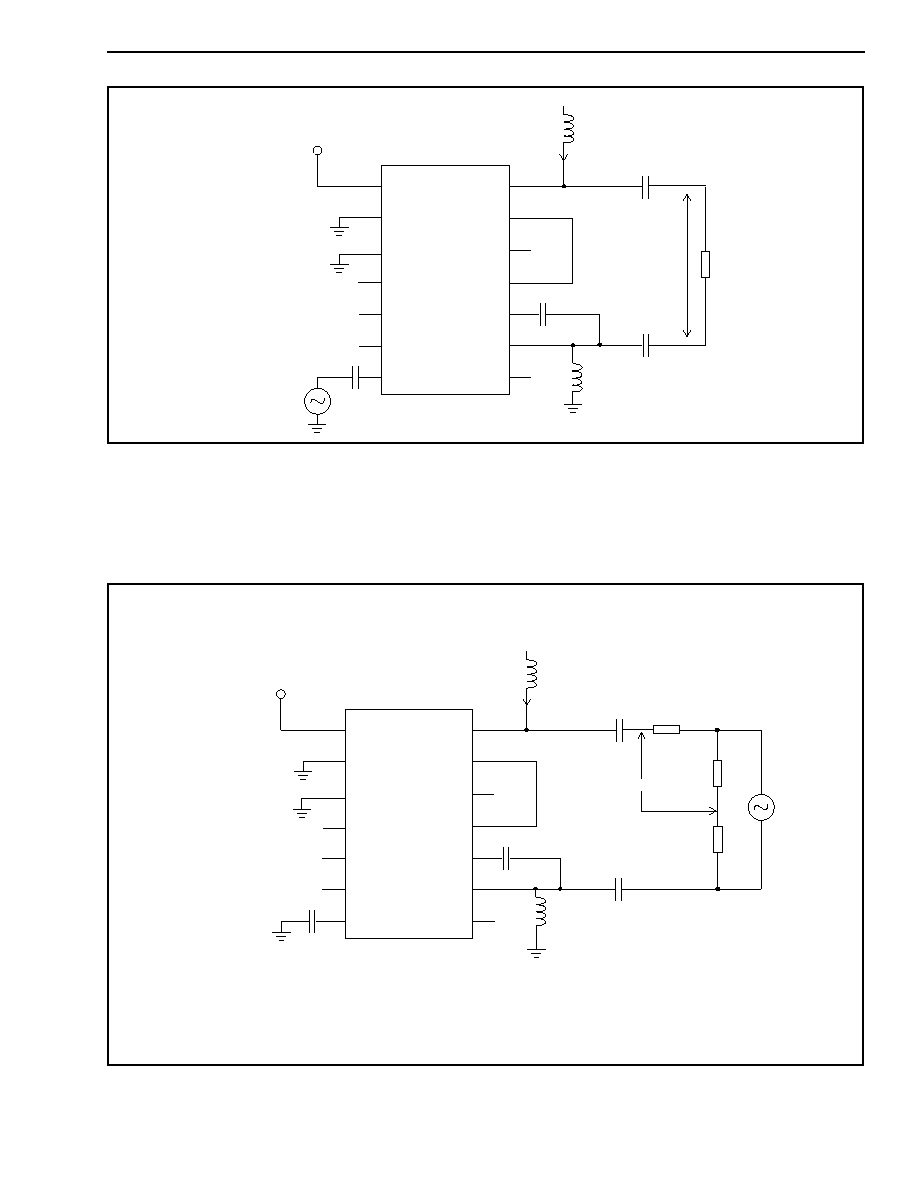
Figure 6 - Test Circuit 3
Figure 7 - Test Circuit 4
DUT
+5v
1
3
5
7
9
11
13
14
16
18
20
22
24
26
VDD
AGND
LC/
RVLC/
NC
VX
VR
TIP
RLS
IC
TF
TXIN
RING
NC
1uF
100uF
470nF
Zin
10H 500
-V
I=20mA
10H 500
100uF
+
+
Vs
Gain = 20 * Log (V(Zin) / Vs)
V (Zin)
DUT
+5v
1
3
5
7
9
11
13
14
16
18
20
22
24
26
VDD
AGND
LC/
RVLC/
IC
VX
VR
TIP
RLS
IC
TF
TXIN
RING
IC
1uF
100uF
470nF
-V
10H 500
I=20mA
V1
300
300
Vs
+
100uF
+
Return Loss = 20 x Log (V1 / Vs)
10H 500
Zin

MH88422
Preliminary Information
2-24
Figure 8 - Test Circuit 5
Figure 9 - Test Circuit 6
DUT
+5v
1
3
5
7
9
11
13
14
16
18
20
22
24
26
VDD
AGND
LC/
RVLC/
IC
VX
VR
TIP
RLS
IC
TF
TXIN
RING
IC
1uF
100uF
470nF
Vs
300
300
-V
10H 500
I=20mA
+
+
100uF
Long. to Met. Balance = 20 * Log (V1 / Vs)
V1
10H 500
DUT
+5v
1
3
5
7
9
11
13
14
16
18
20
22
24
26
VDD
AGND
LC/
RVLC/
IC
VX
VR
TIP
RLS
IC
TF
TXIN
RING
IC
1uF
470nF
-V
10H 500
I=20mA
300
300
V1
Vs
100uF
+
100uF
+
Met. to Long. Balance = 20 * Log (V1 / Vs)
10H 500
510

Preliminary Information
MH88422
2-25
Figure 10 - Mechanical Data for 26-Pin DIL Hybrid
Notes:
1.42 Max
(36.1 Max)
0.19 Max (4.8 Max)
0.10 Typ
(2.54 Typ)
0.020 + 0.005
(0.5 + 0.12)
0.063 Max
0.26+0.015
(22.9 Typ)
0.95 Max
(24.2 Max)
0.90 Typ
0.27 Max
(6.9 Max)
0.08 Typ (2 Typ)
0.20+0.01
(5.08+0.25)
*
*
1
*
(1.6 Max)
(6.6+0.4)
1) Not to scale
2) Dimensions in inches.
(Dimensions in millimetres)
3) Pin tolerances are non-accumulative.
4) Recommended soldering conditions:
Wave soldering - Max temp at pins 260
∞
C for 10 secs.
* Dimensions to centre of pin.
5) Short-cropped pins differ between variants.
(see pin description) 1 & BD-1 variant short.

M Mitel (design) and ST-BUS are registered trademarks of MITEL Corporation
Mitel Semiconductor is an ISO 9001 Registered Company
Copyright 1999 MITEL Corporation
All Rights Reserved
Printed in CANADA
TECHNICAL DOCUMENTATION - NOT FOR RESALE
World Headquarters - Canada
Tel: +1 (613) 592 2122
Fax: +1 (613) 592 6909
North America
Asia/Pacific
Europe, Middle East,
Tel: +1 (770) 486 0194
Tel: +65 333 6193
and Africa (EMEA)
Fax: +1 (770) 631 8213
Fax: +65 333 6192
Tel: +44 (0) 1793 518528
Fax: +44 (0) 1793 518581
http://www.mitelsemi.com
Information relating to products and services furnished herein by Mitel Corporation or its subsidiaries (collectively "Mitel") is believed to be reliable. However, Mitel assumes no
liability for errors that may appear in this publication, or for liability otherwise arising from the application or use of any such information, product or service or for any infringement of
patents or other intellectual property rights owned by third parties which may result from such application or use. Neither the supply of such information or purchase of product or
service conveys any license, either express or implied, under patents or other intellectual property rights owned by Mitel or licensed from third parties by Mitel, whatsoever.
Purchasers of products are also hereby notified that the use of product in certain ways or in combination with Mitel, or non-Mitel furnished goods or services may infringe patents or
other intellectual property rights owned by Mitel.
This publication is issued to provide information only and (unless agreed by Mitel in writing) may not be used, applied or reproduced for any purpose nor form part of any order or
contract nor to be regarded as a representation relating to the products or services concerned. The products, their specifications, services and other information appearing in this
publication are subject to change by Mitel without notice. No warranty or guarantee express or implied is made regarding the capability, performance or suitability of any product or
service. Information concerning possible methods of use is provided as a guide only and does not constitute any guarantee that such methods of use will be satisfactory in a specific
piece of equipment. It is the user's responsibility to fully determine the performance and suitability of any equipment using such information and to ensure that any publication or
data used is up to date and has not been superseded. Manufacturing does not necessarily include testing of all functions or parameters. These products are not suitable for use in
any medical products whose failure to perform may result in significant injury or death to the user. All products and materials are sold and services provided subject to Mitel's
conditions of sale which are available on request.