2-39
Features
∑
FAX and Modem interface V.34(33k6)
∑
Externally programmable line and network
balance impedances
∑
Programmable DC termination characteristics
∑
IEC950 recognised component
∑
Transformerless 2-4 Wire conversion
∑
Integral Loop Switch
∑
Dial Pulse and DTMF operation
∑
Accommodates parallel phone detection
∑
Line state detection outputs:-
loop current/ringing voltage/line voltage
∑
Single +5V operation, low on-hook power
(35mW)
∑
Full duplex voice and data transmission
∑
On-Hook reception from the line
∑
Approvable to UL1950
∑
Industrial temperature range available
Applications
Interface to Central Office or PABX line for:
∑
FAX/Modem (including software modems)
∑
Electronic Point of Sale
∑
Security System
∑
Telemetry
∑
Set Top Boxes
Description
The Mitel MH88435 Data Access Arrangement
(D.A.A.) provides a complete interface between
audio or data transmission equipment and a
telephone line. All functions are integrated into a
single thick film hybrid module which provides high
voltage isolation, very high reliability and optimum
circuit design, needing a minimum of external
components.
The impedance and network balance are externally
programmable, as are the DC termination
characteristics, making the device suitable for most
countries worldwide.
Figure 1 - Functional Block Diagram
Opto-
Isolation
Logic Input
Buffer
Isolation
Isolation
Isolation
Analog
Buffer
Analog
Buffer
Buffer
THL cancellation
impedance
matching circuit
Isolation Barrier
VCC
AGND
LC
VR+
VX
RV
TIP
RING
User Connections
Network Connections
Input Buffer
&
Ring & Loop
Line Termination
VLOOP2
VR-
NB1
NB2
LOOP
LCD
ZA
RS
VBIAS
and line
VLOOP1
DS5132
ISSUE 8
July 1999
Package Information
MH88435AD-P
28 Pin DIL Package
MH88435AS-P
28 Pin SM Package
0
∞
C to +70
∞
C
MH88435AS-PI
28 Pin SM Package
MH88435AD-PI
28 Pin DIL Package
-40
∞
C to +85
∞
C
MH88435-P
Data Access Arrangement
Preliminary Information

MH88435-P
Preliminary Information
2-40
Figure 2 - Pin Connections
Pin Description
Pin #
Name
Description
1
NB1
Network Balance 1. External passive components must be connected between this pin
and NB2.
2
NB2
Network Balance 2. External passive components must be connected between this pin
and NB1.
3
VR+
Differential Receive (Input). Analog input from modem/fax chip set.
4
VR-
Differential Receive (Input). Analog input from modem/fax chip set.
5
VX
Transmit (Output). Ground referenced (AGND) output to modem/fax chip set, biased at
+2.0V.
6
LC
Loop Control (Input). A logic 1 applied to this pin activates internal circuitry which
provides a DC termination across Tip and Ring. This pin is also used for dial pulse
application.
7
ZA
Line Impedance. Connect impedance matching components from this pin to Ground
(AGND).
8
AGND
Analog Ground. 4-Wire ground. Connect to earth.
9
V
CC
Positive Supply Voltage. +5V.
10
VBIAS
Internal Reference Voltage. +2.0V reference voltage. This pin should be decoupled
externally to AGND, typically with a 10
µ
F
6.3V capacitor
.
11
LOOP
Loop (Output). The output voltage on this pin is proportional to the line voltage across Tip
- Ring, scaled down by a factor of 50.
12,
14,
17,
20,
23,
26
IC
Internal Connection. No connection should be made to this pin externally.
13
RS
Ringing Sensitivity. Connecting a link or resistor between this pin and LOOP (pin 11) will
vary the ringing detection sensitivity of the module.
15
LCD
Loop Condition Detect (Output). Indicates the status of loop current.
16
RV
Ringing Voltage Detect (Output). The RV output indicates the presence of a ringing
voltage applied across the Tip and Ring leads.
IC
IC
LC
IC
TIP
AGND
RING
RV
ZA
VX
VR-
VCC
1
2
3
4
5
6
7
8
9
10
11
12
13
14
28
27
26
25
24
23
22
21
20
19
18
17
16
15
VR+
NB1
NB2
VBIAS
LOOP
IC
RS
IC
VLOOP1
VLOOP2
IC
NP
NP
LCD
SC
SC

Preliminary Information
MH88435-P
2-41
18,
19
NP
No Pin. Isolation barrier, no pin fitted in this position.
21,
22
SC
Short Circuit. These two pins should be connected to each other via a 0
link.
24
VLOOP2
Loop Voltage Control Node 2. Used to set DC termination characteristics.
25
VLOOP1
Loop Voltage Control Node 1. Used to set DC termination characteristics.
27
RING
Ring Lead. Connects to the "Ring" lead of the telephone line.
28
TIP
Tip Lead. Connects to the "Tip" lead of the telephone line.
Pin Description (continued)
Functional Description
The device is a Data Access Arrangement (D.A.A.). It
is used to correctly terminate a 2-Wire telephone
line. It provides a signalling link and a 2-4 Wire line
interface between an analog loop and subscriber
data transmission equipment, such as Modems,
Facsimiles (Fax's), Remote Meters, Electronic Point
of Sale equipment and Set Top Boxes.
Isolation Barrier
The device provides an isolation barrier capable of
meeting the supplementary barrier requirements of
the international standard IEC 950 and the national
variants of this scheme such as EN 60950 for
European applications and UL 1950 for North
American applications and is classified as a Telecom
Network Voltage (TNV) circuit.
External Protection Circuit
An External Protection Circuit assists in preventing
damage to the device and the subscriber equipment,
due to over-voltage conditions. See Application Note,
MSAN-154 for recommendations.
Suitable Markets
The MH88435 has features such as programmable
input and network balance impedance,
programmable DC termination and a supplementary
isolation barrier that makes it ideal for use
throughout the world.
There are a small number of countries with a 100M
leakage requirement that this device does not meet.
These are Belgium, Greece, Italy, Luxembourg and
Spain.
France's current limit specification and Germany's
dial pulse requirements are met by the MH88437.
This device is pin for pin compatible with the
MH88435.
Approval specifications are regularly changing and
the relevant specification should always be consulted
before commencing design.
Line Termination
When Loop Control (LC) is at a logic 1, a line
termination is applied across Tip and Ring. The
device is off-hook and DC loop current will flow. The
line termination consists of both a DC line
termination and an AC input impedance. It is used to
terminate an incoming call, seize the line for an
outgoing call, or if it is applied and disconnected at
the required rate, can be used to generate dial
pulses.
The DC termination is approximately 300
resistance, which is loop current dependent. It can
be programmed to meet different national
requirements. For normal operation Pin 22 and Pin
21 should be linked, and a resistor (R2) should be
fitted between VLOOP1 and VLOOP2 as shown in
Figure 5.
The approval specification will give a DC mask
characteristic that the equipment will need to comply
to. The DC mask specifies the amount of current the
DAA can source for a given voltage across tip and
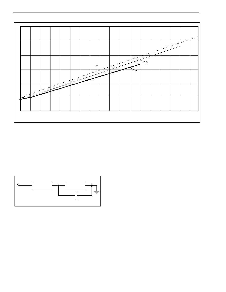
ring. Figure 3 shows how the voltage across tip and
ring varies with different resistors (R2) for a given
loop current.
The AC input impedance should be set by the user to
match the line impedance.

MH88435-P
Preliminary Information
2-42
Input Impedance
The MH88435 has a programmable input impedance
set by fitting external components between the ZA
pin and AGND.
For complex impedances the configuration shown in
Figure 4 is most commonly found.
Figure 4 - Complex Impedances
To find the external programming components for
configuration 4, the following formula should be
used:
Zext = [(10 x R1)-1k3]+ [10 x R2)//(C1/10)]
e.g. If the required input impedance = 220
+
(820
//115nF), the external network to be connected
to ZA will be:
Zext = 900
+
(8k2
//12nF)
Where the input impedance (Z) = 600R the equation
can be simplified to:
Zext = (10 x Z) - 1k3
Zext = 4k7
Note: A table of commonly used impedances can be
found in the DAA Application's document MSAN-154.
Zext = external network connected between ZA and
AGND, Zint = 1.3k
(internal resistance).
Network Balance
The network balance impedance of the device can
be programmed by adding external components
between NB1 and NB2. For countries where the
balance impedance matches the line impedance, a
15k
resistor should be added between NB1 and
NB2.
Ringing Voltage Detection
The sensitivity of the ringing voltage detection
circuitry can be adjusted by applying an external
resistor between the RS and LOOP pins. With a
short circuit, the threshold sensitivity is ~10Vrms R7
can be calculated using the equation:
R1
R2
C1
ZA
Iloop=26mA
Iloop=20mA
Iloop=15mA
10
5
0
25
20
15
30
R2(kOhms)
200 600 1000 1400 1800 2200 2600 3000 3400 3800
Figure 3 - DC Programming Capabilities
(V(t-r)

Preliminary Information
MH88435-P
2-43
R7 = 30 k
x (Desired Threshold Voltage - 10Vrms)
Therefore, 300k k
gives ~ 20Vrms and 600k k
gives ~ 30Vrms
An AC ringing voltage across Tip and Ring will cause
RV to output TTL pulses at the ringing frequency,
with an envelope determined by the ringing cadence.
Parallel Phone and Dummy Ringer
An external parallel phone or dummy ringer circuit
can be connected across Tip and Ring as shown in
Figure 5. A dummy ringer is an AC load which
represents a telephone's mechanical ringer.
In normal circumstances when a telephone is on-
hook and connected to the PSTN, its AC (Ringer)
load is permanently presented to the network. This
condition is used by many PTT's to test line
continuity by placing a small AC current onto the line
and measuring the voltage across tip (A) and ring
(B).
Today's telecom equipment may not have an AC load
present across tip and ring (e.g. modems), therefore
any testing carried out by the PTT will see an open
circuit across tip and ring. In this instance the PTT
assumes that the line continuity has been damaged.
To overcome this problem many PTT's specify that a
"Dummy Ringer" is presented to the network at all
times. Ideally its impedance should be neglible in
the audio band, and high at the ringing frequencies
(e.g. 25Hz). Note that the requirement for the
"Dummy Ringer" is country specific.
Parallel phone detection is used mostly in set-top
box applications. This is when a modem call will
need to be disconnected from the central office by
the equipment when the parallel phone is in the off-
hook state. This is so that a call can be made to the
emergency services.
To detect this state, additional circuitry will be
required and can be found in the application note,
MSAN-154.
2-4 Wire Conversion
The device converts the balanced 2-Wire input,
presented by the line at Tip and Ring, to a ground
referenced signal at VX, biased at 2.0V. This
simplifies the interface to a modem chip set.
Conversely, the device converts the differential signal
input at VR+ and VR- to a balanced 2-Wire signal
across Tip and Ring. The device can also be used in
a single ended mode at the receive input, by leaving
VR+ open circuit and connecting the input signal to
VR- only. Both inputs are biased at 2.0V.
During full duplex transmission, the signal at Tip and
Ring consists of both the signal from the device to
the line and the signal from the line to the device.
The signal input at VR+ and VR- being sent to the
line, must not appear at the output VX. In order to
prevent this, the device has an internal cancellation
circuit. The measure of this attenuation is
Transhybrid Loss (THL).
The MH88435 has the ability to transmit analog
signals from Tip and Ring through to VX when on-
hook. This can be used when receiving caller line
identification information.
Transmit Gain
The Transmit Gain of the MH88435 is the gain from the
differential signal across Tip and Ring to the ground
referenced signal at VX. The internal Transmit Gain of
the device is fixed as shown in the AC Electrical
Characteristics table. For the correct gain, the Input
Impedance of the MH88435, must match the specified
line impedance.
By adding an external potential divider to VX, it is
possible to reduce the overall gain in the application.
The output impedance of VX is approximately 10
and
the minimum resistance from VX to ground should be
2k
.
Example: If R3 = R4 = 2k
,
in Figure 5, the overall
gain would reduce by 6.0dB.

MH88435-P
Preliminary Information
2-44
Receive Gain
The Receive Gain of the MH88435 is the gain from
the differential signal at VR+ and VR- to the
differential signal across Tip and Ring. The internal
Receive Gain of the device is fixed as shown in the
AC Electrical Characteristics table. For the correct
gain, the Input Impedance of the MH88435 must
match the specified line impedance.
With an internal series input resistance of 47k
at
the VR+ and VR- pins, external series resistors can
be used to reduce the overall gain.
Overall Receive Gain = 0dB + 20log (47k
/
(47k
+R5)).
For differential applications R6 must be equal to R5
in Figure 5.
Example: If R5 = R6 = 47k in Figure 5, the overall
gain would reduce by 6.0dB.
Supervisory Features
The device is capable of monitoring the line
conditions across Tip and Ring, this is shown in
Figure 5. The Loop Condition Detect pin (LCD),
indicates the status of the line. The LCD output is at
logic 1 when loop current flows, indicating that the
MH88435 is in an off-hook state. LCD will also go
high if a parallel phone goes off-hook while the DAA
is on-hook. Therefore, line conditions can be
determined with the LC and the LCD pins.
The LOOP pin output voltage, VLoop, is proportional
to the line voltage across Tip and Ring, V (t-r),
scaled down by a factor of 50 and offset by VBias
which is approximately 2V. With the aid of a simple
external detector the LC, LCD and LOOP pins can
be used to generate the signals necessary for
parallel phone operation with a Set Top Box. Refer to
MSAN-154.
If Tip is more positive than ring VLoop < VBias
If Tip is more negative than ring VLoop > VBias
V (t-r)
(VLoop - VBias) * 50
When the device is generating dial pulses, the LCD
pin outputs TTL pulses at the same rate. The LCD
output will also pulse if a parallel phone is used to
pulse dial and also when ringing voltage is present at
Tip and Ring.
Mechanical Data
See Figure 12, 13 and 14 for details of the
mechanical specification.

Preliminary Information
MH88435-P
2-45
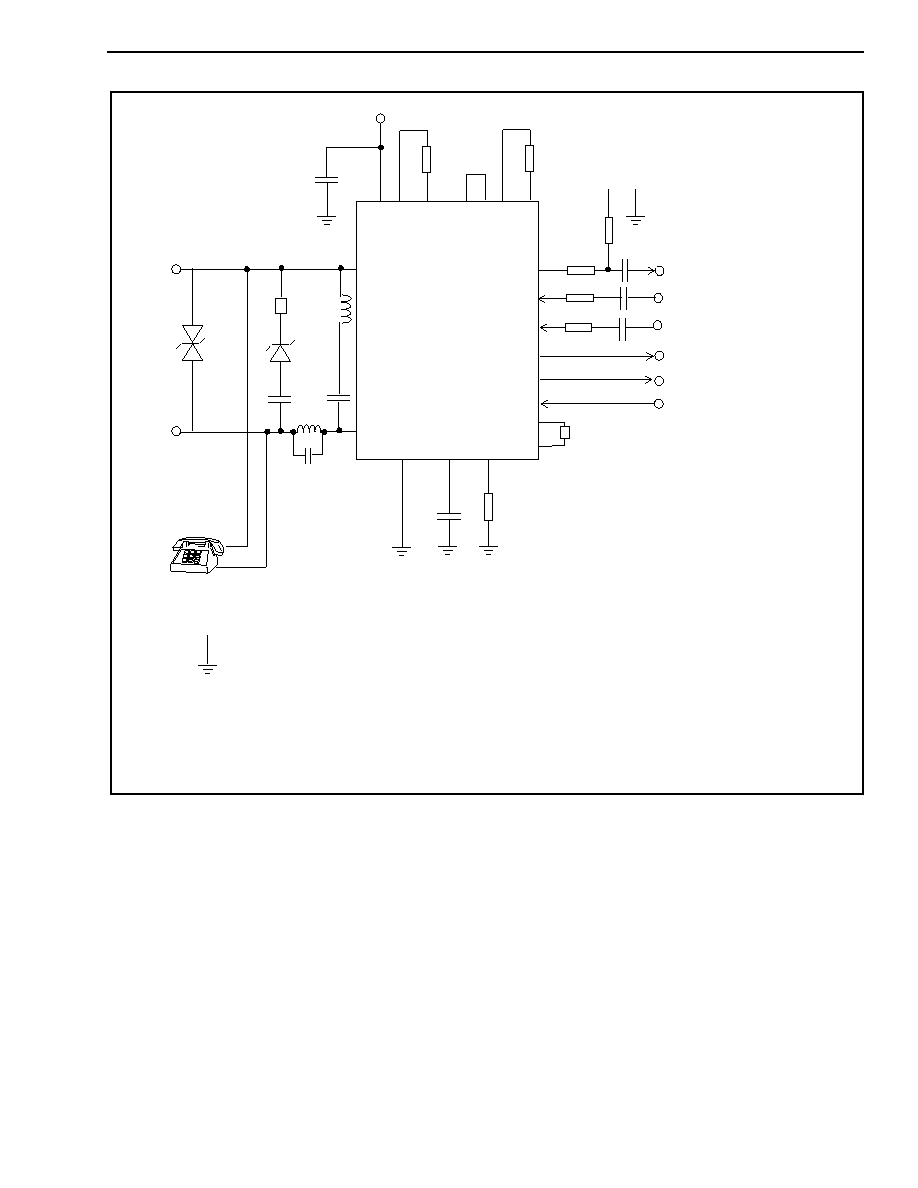
Figure 5 - Typical Application Circuit
TIP
NB2
RING
VX
VR+
RV
LC
AGND
VCC
TIP
RING
C2
+5V
9
8
6
16
5
3
27
28
Analog
Input
Analog
Ringing Voltage Detect Output
Loop Control Input
MH88435
+
Output
C3
C1
Notes:
1) R1 & C1: Dummy Ringer, country specific
ZA
7
Zext
2) R2: DC Mask Resistor typical 360k
R1
25
24
VLOOP1
VLOOP2
VR-
4
Analog
Input
R2
LCD
15
Loop Current Detect Output
NB1
5) ZB: Network Balance Impedance
R3
R5
R6
R4
4) R5 = R6: Receive Gain Resistors typically 100k
3) R3 & R4: Transmit Gain Resistors
2k2
C6 +
10
VBIAS
typically 0.39
µ
F, 250V & 3k
6) C2, C6 = 10
µ
F 6V
7) C7 & C8 = 39nF for 12kHz filter and 22nF for
16KHz filter. These can be left off if meter pulse
filtering not required.
8) Zext: External Impedance
9) D1 Zener Diode 6V2
10) L1, L2 = 4m7H 80mA. These can be left off if
meter pulse filtering not required.
D1
C7
L1
L2
C8
13 11
RS
LOOP
ZB
1
2
C4
C5
11) C3, C4 & C5 = 1
µ
F coupling capacitors
12) R7 = 620k
(30V RMS ringing sensitivity)
D2
R7
13) D2 = Teccor P3100SB
= Ground (Earth)
22 21

MH88435-P
Preliminary Information
2-46
.
*Exceeding these values may cause permanent damage. Functional operation under these conditions is not implied.
Typical figures are at 25∞C with nominal +5V supply and are for design aid only
Electrical Characteristics are over Recommended Operating Conditions unless otherwise stated.
Typical figures are at 25
∞
C with nominal + 5V supplies and are for design aid only.
Note 1: Refer to EIA/TIA 464 section 4.1.1.4.4.
Note 2: This is equivalent to 10M
leakage Tip/Ring to Ground. For countries requiring 100M
leakage use the MH88436 with an
enhanced leakage specification.
Note 3: Operation at low loop currents depends on the DC programming resistor between VLoop1/2. The recommended 360K value
will support V34 operation down to 20mA. Voice operation is supported down to 15mA.
Absolute Maximum Ratings* -
All voltages are with respect to AGND unless otherwise specified.
Parameter
Sym
Min
Max
Units
Comments
1
DC Supply Voltage
V
CC
-0.3
6
V
2
Storage Temperature
T
S
-55
+125
∞C
3
DC Loop Voltage
V
BAT
-110
+110
V
4
Ringing Voltage
V
R
150
Vrms
VBAT = -56V
5
Loop Current
I
Loop
90
mA
6
Ring Trip Current
I
TRIP
180
mA
rms
250ms 10% duty cycle or
500ms single shot
Recommended Operating Conditions
Parameter
Sym
Min
Typ
Max
Units
Test Conditions
1
DC Supply Voltages
V
CC
4.75
5.0
5.25
V
2
Operating Temperatures
Industrial Temperature
T
OP
0
-40
25
70
+85
∞C
3
Ringing Voltage
V
R
75
90
Vrms
Loop Electrical Characteristics
-
Characteristics
Sym
Min
Typ
Max
Units
Test Conditions
1
Ringing Voltage threshold
VR
7
10
14
Vrms
Externally Adjustable
2
Ringing Frequency
15
68
Hz
3
Operating Loop Current
15
80
mA
Note 3
4
Off-Hook DC Voltage
Tip/Ring
6.0
6.0
7.8
V
V
V
Test circuit as Fig. 4
I
Loop
=15mA )Note 1
I
Loop
=20mA )where R2
=I
Loop
=26mA ) 360k
5
Leakage Current
(Tip or Ring to AGND)
10
7
µ
A
mA
rms
100V DC Note 2.
1000V AC
6
Leakage Current on-hook
(Tip to Ring)
9
10
µ
A
V
BAT
= -50V
7
Dial Pulse Delay ON
OFF
0
0
+2
+2
+4
+4
ms
ms
8
Loop Condition Detect Threshold
Off-Hook
5
16
V
Voltage across tip and
ring

Preliminary Information
MH88435-P
2-47
Electrical Characteristics are over Recommended Operating Conditions unless otherwise stated.
Typical figures are at 25
∞
C with nominal + 5V supplies and are for design aid only.
Variations from Standard Loop Electrical Characteristics -
(MH88435AD-PI/MH88435AS-PI)
Characteristics
Sym
Min
Typ
Max
Units
Test Conditions
1
Ringing Voltage Threshold
VR
17
Vrms
-40∞C to 0∞C
2
Operating Loop Current
22
80
mA
-40∞C to 0∞C
+70∞C to +85∞C
DC Electrical Characteristics
Characteristics
Sym
Min
Typ
Max
Units
Test Conditions
1
Supply Current
I
CC
7
mA
V
CC
= 5.0V, On-hook
2
RV,
LCD
Low Level Output Voltage
High Level Output Voltage
V
OL
V
OH
2.4
0.4
V
V
I
OL
= 4mA
I
OH
= 0.4mA
3
LC
Low Level Input Voltage
High Level Input Voltage
Low Level Input Current
High Level Input Current
V
IL
V
IH
I
IL
I
IH
2.0
0
350
0.8
10
400
V
V
µ
A
µ
A
V
IL
= 0.0V
V
IH
= 5.0V
AC Electrical Characteristics
Characteristics
Sym
Min
Typ
Max
Units
Test Conditions
1
Input Impedance VR-
VR+
47k
94k
2
Output Impedance at VX
10
3
Receive Gain (VR to 2-Wire)
-1
0
1
dB
Test circuit as Fig. 8
Input 0.5V at 1kHz
4
Frequency Response Gain
(relative to Gain @ 1kHz)
-0.5
-0.5
+0.4
0
+0.5
+0.5
dB
dB
300Hz
3400Hz
5
Signal Output Overload Level
at 2-Wire
at VX
0
0
dBm
dBm
THD < 5% @ 1kHz
I
LOOP
= 25-75mA
6
Signal/Noise & Distortion
at 2-Wire
at VX
SINAD
70
70
dB
dB
Input 0.5V at 1kHz
I
LOOP
= 25-75mA
300-3400Hz
7
Power Supply Rejection Ratio
at 2-Wire
at VX
PSRR
25
25
40
40
dB
dB
Ripple 0.1Vrms 1kHz
on V
CC
8
Transhybrid Loss
THL
16
25
dB
Test circuit as Fig.8
300-3400Hz at V
R
9
2-Wire Input Impedance
Zin
Note 3
@1kHz
10
Return Loss at 2-Wire
(Reference 600
)
RL
14
20
18
20
24
24
dB
dB
dB
Test circuit as Fig. 9
200-500Hz
500-2500Hz
2500-3400Hz

MH88435-P
Preliminary Information
2-48
Electrical Characteristics are over Recommended Operating Conditions unless otherwise stated.
Typical figures are at 25
∞
C with nominal +5V and are for design aid only.
Note 1: All of the above test conditions use a test source impedance which matches the device's impedance.
Note 2: dBm is referenced to 600
unless otherwise stated
.
Note 3: These parameters need to be taken into consideration when designing or specifying the power supply.
11
Longitudinal to Metallic Balance
Metallic to Longitudinal Balance
46
46
60
40
65
65
68
62
dB
dB
dB
dB
Test circuit as Fig. 10
300-1000Hz
1000-3400Hz
Test circuit as Fig.11
200-1000Hz
1000-4000Hz
12
Idle Channel Noise
at 2-Wire
at VX
at 2-Wire
at VX
Nc
10
10
-80
-80
20
20
dBrnC
dBrnC
dBm
dBm
Cmess filter
300-3400Hz filter
13
Transmit Gain (2-Wire to VX)
(Terminated gain) Off-Hook
(Voltage gain) On-Hook
-1
0
0
+1
dB
dB
Test circuit as Fig. 7
Input 0.5V @ 1kHz
LC = 0V
14
Frequency Response Gain
(relative to Gain @ 1kHz)
-1
-1
+0.3
+0.2
+1
+1
dB
dB
300Hz
3400Hz
15
Intermodulation Distortion
products at VX and 2W
IMD
60
dB
I
LOOP
= 25-75mA
F1 = 1kHz at -6dBm
F2 = 800Hz at -6dBm
Total signal power =
-3dBm
16
Distortion at VX due to near end
echo
(300Hz - 3400Hz bandwidth)
75
dB
I
LOOP
= 25-75mA
F1 = 1kHz at -6dBm
F2 = 800Hz at -6dBm
Total signal power =
-3dBm
17
Common Mode Rejection on 2 wire
at VX
CMRR
56
dB
Test circuit as Fig. 10
1-100Hz. Note 4
18
Common Mode overload level
CMOL
7
Vrms
Test circuit as Fig. 10.
Note 4
Variations from Standard AC Electrical Characteristics
(MH88437AD-PI/MH88437AS-PI) (-40∞C to 0∞C)
Characteristics
Sym
Min
Typ
Max
Units
Test Conditions
1
Frequency Response Gain
-0.6
-0.65
dB
300Hz (-40∞C to 0∞C)
AC Electrical Characteristics
Characteristics
Sym
Min
Typ
Max
Units
Test Conditions

Preliminary Information
MH88435-P
2-49
Figure 6 - Test Circuit 1
Figure 7 - Test Circuit 2
MH88435
3
4
5
25
VX
AGND
RV
VR+
VR-
TIP
NB1
RING
24
22
21
360K
VLOOP1
LC
5V
1K
VLOOP2
VCC ZA
NB2
10uF
VBIAS
10
27
2
28
1
15K
6
16
8
7
9
4.7K
LOOP
RS
LCD
11
13
15
ILOOP
5V
= Ground (Earth)
SC
SC
Vs
I=20mA
10H 500
-V
100uF
10H 500
+
100uF
+
Gain = [20 * Log (VX / Vs)] + 6.02 dB
MH88435
3
4
5
25
VX
AGND
RV
VR+
VR-
TIP
NB1
RING
24
22
21
360K
VLOOP1
LC
5V
1K
VLOOP2
VCC ZA
NB2
10uF
VBIAS
10
27
2
28
1
15K
6
16
8
7
9
4.7K
5V
LOOP
RS
LCD
11
13
15
Impedance = Zin
= Ground (Earth)
SC
SC

MH88435-P
Preliminary Information
2-50
Figure 8 - Test Circuit 3
Figure 9 - Test Circuit 4
100uF
Zin
10H 500
-V
I=20mA
10H 500
100uF
+
+
Gain = 20 * Log (V(Zin) / Vs)
MH88435
3
4
5
25
VX
AGND
RV
VR+
VR-
TIP
NB1
RING
24
22
21
360K
VLOOP1
LC
5V
1K
VLOOP2
VCC ZA
NB2
10uF
VBIAS
10
27
2
28
1
15K
6
16
8
7
9
4.7K
5V
LOOP
RS
LCD
11
13
15
Vs
= Ground (Earth)
SC
SC
100uF
-V
10H 500
I=20mA
V1
300
300
Vs = 0.5V
+
100uF
+
Return Loss = 20 * Log (2V1 / Vs)
10H 500
Zin
MH88435
3
4
5
25
VX
AGND
RV
VR+
VR-
TIP
NB1
RING
24
22
21
360K
VLOOP1
LC
5V
1K
VLOOP2
VCC ZA
NB2
10uF
VBIAS
10
27
2
28
1
15K
6
16
8
7
9
4.7K
LOOP
RS
LCD
11
13
15
5V
= Ground (Earth)
SC
SC

Preliminary Information
MH88435-P
2-51
Figure 10 - Test Circuit 5
Figure 11 - Test Circuit 6
100uF
Vs = 0.5V
300
300
-V
10H 500
I=20mA
+
+
100uF
Long. to Met. Balance = 20 * Log (V1 / Vs)
V1
10H 500
MH88435
3
4
5
25
VX
AGND
RV
VR+
VR-
TIP
NB1
RING
24
22
21
360K
VLOOP1
LC
5V
1K
VLOOP2
VCC ZA
NB2
10uF
VBIAS
10
27
2
28
1
15K
6
16
8
7
9
4.7K
5V
LOOP
RS
LCD
11
13
15
CMR = 20 * Log (VX / Vs)
= Ground (Earth)
SC
SC
CMOL = V2
V2
-V
10H 500
I=20mA
300
300
V1
Vs
100uF
+
100uF
+
Met. to Long. Balance = 20 * Log (V1 / Vs)
10H 500
510
MH88435
3
4
5
25
VX
AGND
RV
VR+
VR-
TIP
NB1
RING
24
22
21
360K
VLOOP1
LC
5V
1K
VLOOP2
VCC ZA
NB2
10uF
VBIAS
10
27
2
28
1
15K
6
16
8
7
9
4.7K
5V
LOOP
RS
LCD
11
13
15
= Ground (Earth)
SC
SC

MH88435-P
Preliminary Information
2-52
Figure 12 - Mechanical Data for 28 Pin DIL Hybrid
Figure 13 - Mechanical Data for 28 Pin Surface Mount Hybrid
Notes:
1) Not to scale
2) Dimensions in inches.
(Dimensions in millimetres)
1.42 Max
(36.1 Max)
0.162 Max (4.12 Max)
0.05 Typ
(1.27 Typ)
0.020 + 0.005
(0.5 + 0.13)
0.063 Max
0.260+0.015
(25.4 Typ)
1.05 Max
(26.7 Max)
* Dimensions to centre of pin.
1.00 Typ
0.27 Max
(6.9 Max)
0.08 Typ (2 Typ)
0.100+0.010
(2.54+0.25)
*
*
1
*
(1.6 Max)
(6.6+0.38)
3) Pin tolerances are non-accumulative.
4) Recommended soldering conditions:
Wave Soldering - Max temp at pins 260
∞
C for 10 secs.
0.300+0.010
(7.62+0.25)
*
Notes:
1) Not to scale
2) Dimensions in inches.
(Dimensions in millimetres)
1.42 Max
(36.1 Max)
0.162 Max (4.11 Max)
0.063 Max
* Dimensions to centre of pin.
1
(1.6 Max)
3) Pin tolerances are non-accumulative.
4) Recommended soldering conditions:
0.300+0.010
(7.62+0.25)
*
(25.15 Typ)
0.060 Typ
(1.52 Typ)
0.99 Typ
0.110+0.015
(2.80+0.38)
0.287 Max
(7.29 Max)
0.100+0.010
(2.54+0.25)
*
0.020 + 0.005
(0.5 + 0.13)
0.05 Typ
(1.27 Typ)
*
Max reflow temp: 220
∞
C for 10 secs.
1.15 Max
(29.2 Max)

Preliminary Information
MH88435-P
2-53
Figure 14 - Recommended Footprint for 28 Pin Surface Mount Hybrid
0.10
(2.54)
0.99
(25.15)
0.04
(1.02)
0.06
(1.52)
0.10
(2.54)
0.26
(6.60)
Notes:
1) Not to scale
2) Dimensions in inches.
(Dimensions in millimetres)
3) All dimensions are Typical except
*
where marked with an .This gap is
associated with the isolation barrier.

M Mitel (design) and ST-BUS are registered trademarks of MITEL Corporation
Mitel Semiconductor is an ISO 9001 Registered Company
Copyright 1999 MITEL Corporation
All Rights Reserved
Printed in CANADA
TECHNICAL DOCUMENTATION - NOT FOR RESALE
World Headquarters - Canada
Tel: +1 (613) 592 2122
Fax: +1 (613) 592 6909
North America
Asia/Pacific
Europe, Middle East,
Tel: +1 (770) 486 0194
Tel: +65 333 6193
and Africa (EMEA)
Fax: +1 (770) 631 8213
Fax: +65 333 6192
Tel: +44 (0) 1793 518528
Fax: +44 (0) 1793 518581
http://www.mitelsemi.com
Information relating to products and services furnished herein by Mitel Corporation or its subsidiaries (collectively "Mitel") is believed to be reliable. However, Mitel assumes no
liability for errors that may appear in this publication, or for liability otherwise arising from the application or use of any such information, product or service or for any infringement of
patents or other intellectual property rights owned by third parties which may result from such application or use. Neither the supply of such information or purchase of product or
service conveys any license, either express or implied, under patents or other intellectual property rights owned by Mitel or licensed from third parties by Mitel, whatsoever.
Purchasers of products are also hereby notified that the use of product in certain ways or in combination with Mitel, or non-Mitel furnished goods or services may infringe patents or
other intellectual property rights owned by Mitel.
This publication is issued to provide information only and (unless agreed by Mitel in writing) may not be used, applied or reproduced for any purpose nor form part of any order or
contract nor to be regarded as a representation relating to the products or services concerned. The products, their specifications, services and other information appearing in this
publication are subject to change by Mitel without notice. No warranty or guarantee express or implied is made regarding the capability, performance or suitability of any product or
service. Information concerning possible methods of use is provided as a guide only and does not constitute any guarantee that such methods of use will be satisfactory in a specific
piece of equipment. It is the user's responsibility to fully determine the performance and suitability of any equipment using such information and to ensure that any publication or
data used is up to date and has not been superseded. Manufacturing does not necessarily include testing of all functions or parameters. These products are not suitable for use in
any medical products whose failure to perform may result in significant injury or death to the user. All products and materials are sold and services provided subject to Mitel's
conditions of sale which are available on request.


