 | –≠–ª–µ–∫—Ç—Ä–æ–Ω–Ω—ã–π –∫–æ–º–ø–æ–Ω–µ–Ω—Ç: MH88632 | –°–∫–∞—á–∞—Ç—å:  PDF PDF  ZIP ZIP |
2-235
Æ
Features
∑
Loop start and ground start capabilities
∑
Transformerless 2-4 wire conversion
∑
Programmable transmit/receive gain with 0dB
defaults
∑
Programmable input impedance with 600
and
900
defaults
∑
Programmable network balance with 600
,
900
, and AT&T compromise default
∑
One loop start & two ground start relay drivers
∑
Line state detection outputs
∑
Forward loop, reverse loop, ring ground, tip
ground, ringing voltage
∑
+5V operation
∑
On-hook audio reception (to accommodate ANI)
Applications
I
nterface to Central Office for:
∑
PBX
∑
Key Telephone System
∑
Channel bank
∑
Voice Mail
∑
Terminal Equipment
∑
Digital Loop Carrier
Description
The Mitel MH88632 Central Office Trunk Interface
circuit provides a complete audio and signalling link
between audio switching equipment and a central
office. The functions provided by the MH88632
include 2-4 Wire Hybrid conversion, programmable
transmit and receive gains, programmable line
impedance and programmable network balance. The
device is fabricated using thick film hybrid
technology which incorporates various technologies
for optimum circuit design and very high reliability.
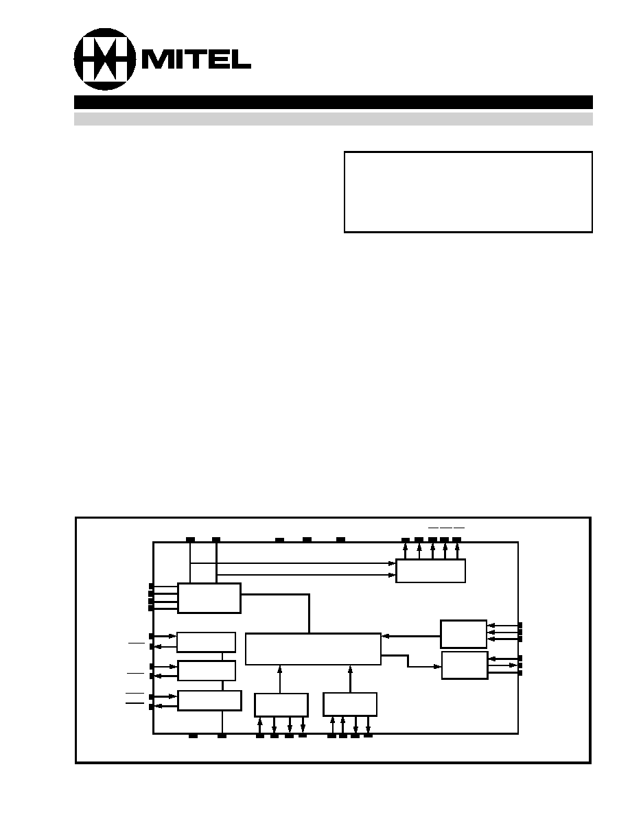
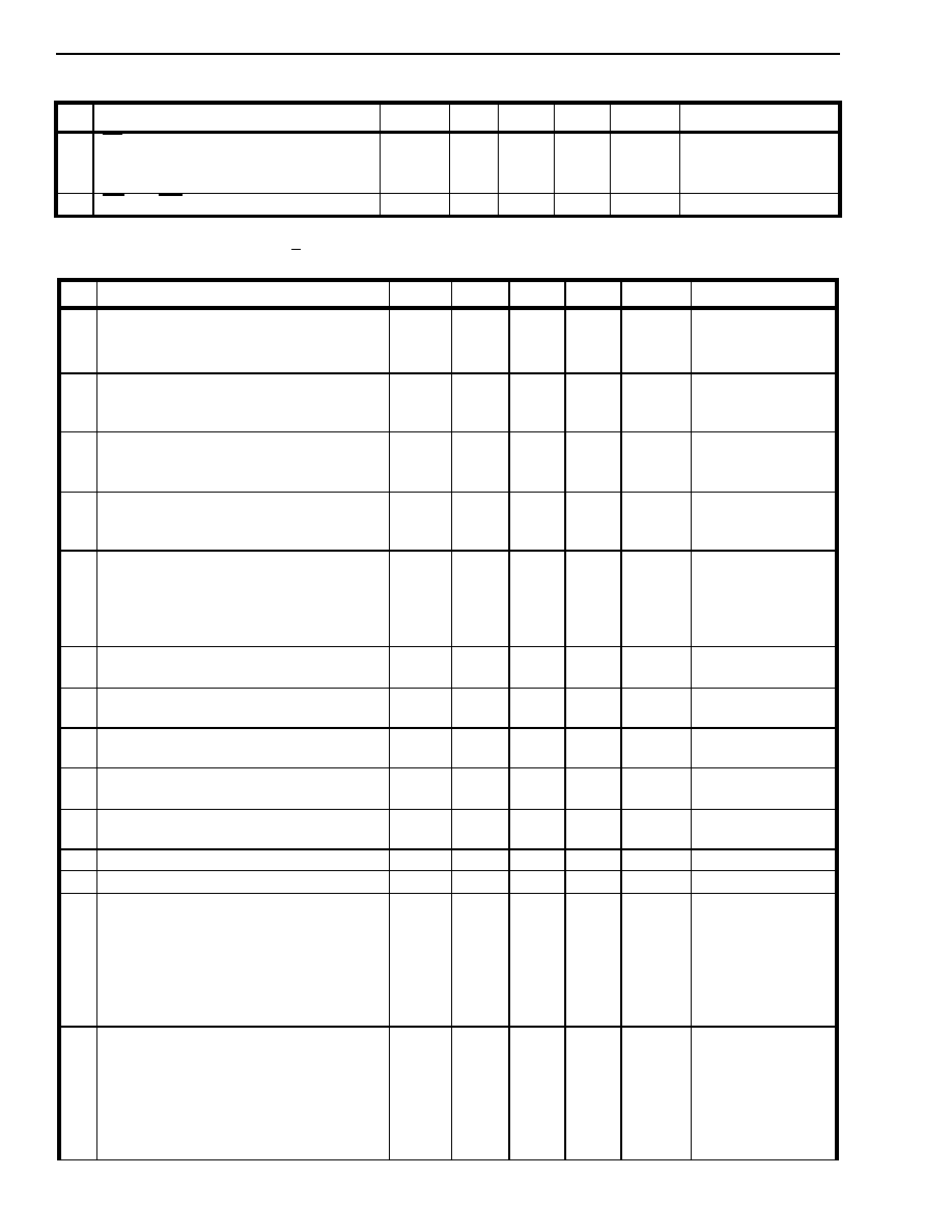
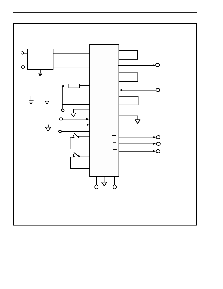
Status
Detection
2-4 Wire Hybrid
Loop
Termination
Loop Relay
Driver
Bias Relay
Driver
Ring Ground
Driver
Impedance
Matching
Receive
Gain
Transmit
Gain
XLA
XLB
XLC
XLD
LRC
LRD
BRC
BRD
GRC
GRD
VRLY
RGND
Z1 Z2 Z600 Z900 NS N1 N2 NATT
TIP
RING
VDD
VEE
AGND
RX
GRX1
GRX0
TX
GTX1
GTX0
RV FL RL RG TG
Network
Balance
ISSUE 5
April 1995
Ordering Information
MH88632 40 Pin SIL Package
0
∞
C to 70
∞
C
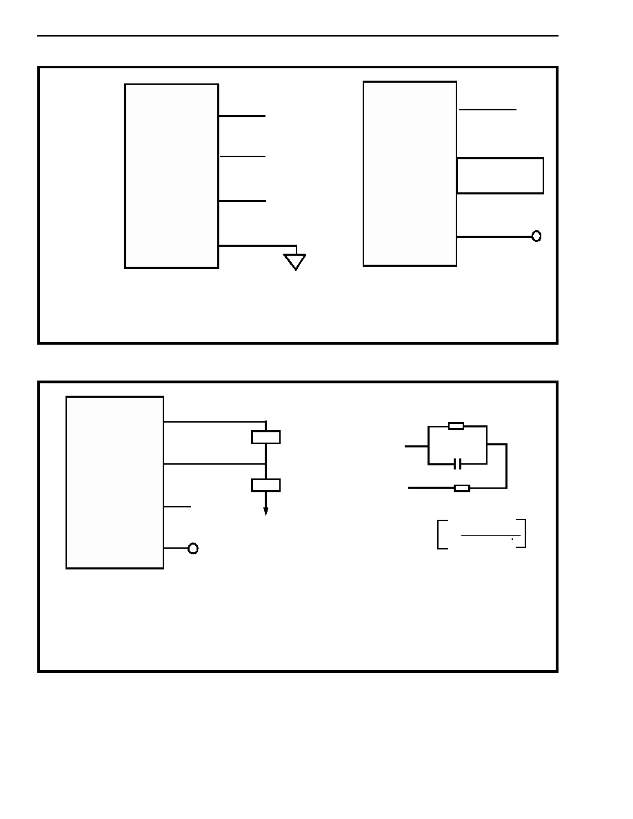
Figure 1 - Functional Block Diagram
MH88632
Central Office Interface Circuit
Preliminary Information
2-236
MH88632
Preliminary Information
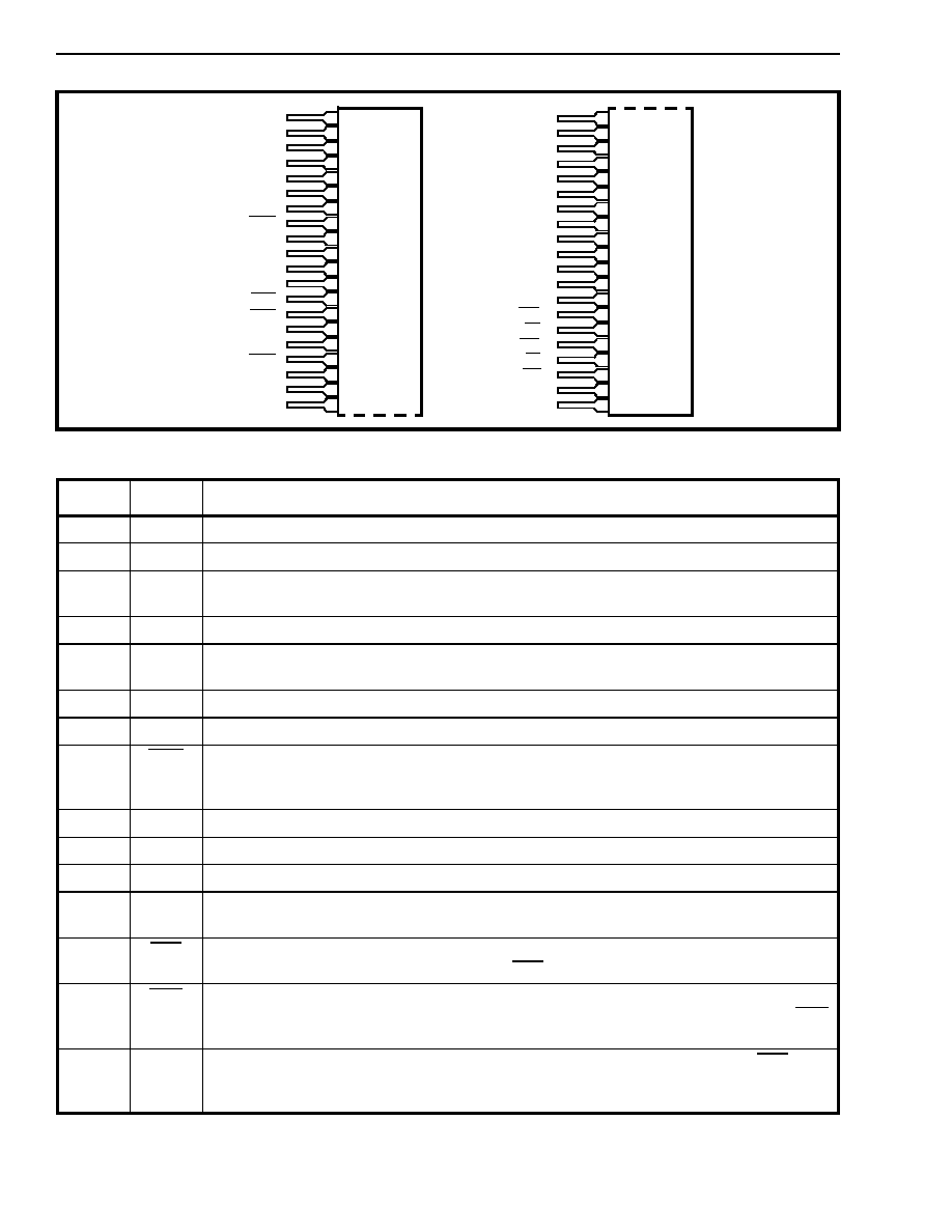
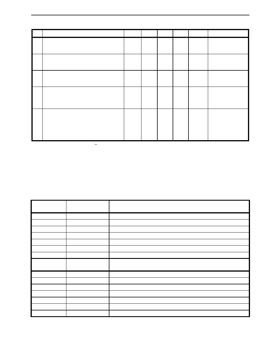
Figure 2 - Pin Connections
Pin Description
Pin #
Name
Description
1
TIP
Tip Lead. Connects to the "Tip" or "Ring" lead of Central Office.
2
RING
Ring Lead. Connects to the "Ring" or "Tip" lead of the Central Office.
3
XLA
Loop Relay Contact A. Connects to XLB through the loop relay (K1) contacts when the
relay is activated. Activates internal active termination circuitry.
4
XLB
Loop Relay Contact B. See XLA for description.
5
XLC
Loop Relay Contact C. Connects to XLD through the loop relay (K1) contacts when the
relay is activated. Activates internal active termination circuitry.
6
XLD
Loop Relay Contact D. See XLC for description
7
IC
Internal Connection.This pin is internally connected and must be left open.
8
GRD
Ground Relay Lead Relay Drive (Output). Connects to the Ground Ring Lead Relay Coil,
used for Ground Start applications. A logic low activates the relay. An internal clamp diode
from VRLY to GND is provided.
9
IC
Internal Connection. This pin is internally connected and must be left open.
10
IC
Internal Connection. This pin is internally connected and must be left open.
11
RGND
Relay Ground. Return path for relay supply voltage.
12
VRLY
Relay Positive Supply Voltage. Normally +5V. Connects to the relay coil and the relay
supply voltage
13
LRD
Loop Relay Drive (Output). Connects to the Bias Relay coil. A logic low activates the
relay. An internal clamp diode from VRLY to LRD is provided.
14
BRD
Bias Relay Drive (Output). Connects to the Bias Relay coil, used for Ground start
applications only. A logic low activates the relay. An internal clamp diode from VRLY to BRD
is provided.
15
LRC
Loop Relay Control (Input). A logic high activates the Loop Relay Drive output (LRD). The
Loop Relay activates internal circuitry which provides a DC termination across Tip and
Ring. Used for line seizure and dial pulsing.
N2
Z900
Z1
Z2
TX
RX
GTX0
GTX1
GRX0
GRX1
IC
Z600
NS
TG
RL
RV
FL
RG
VEE
VDD
TIP
RING
XLA
XLB
XLC
XLD
IC
GRD
IC
IC
RGND
VRLY
LRD
BRD
LRC
BRC
GRC
AGND
NATT
N1
1
2
3
4
5
6
7
8
9
10
11
12
13
14
15
16
17
18
19
20
21
22
23
24
25
26
27
28
29
30
31
32
33
34
35
36
37
38
39
40

2-237
Preliminary Information
MH88632
16
BRC
Bias Relay Control (Input). A logic high activates the Loop Relay Drive output (BRD),
used for Ground start applications only. This input should be connected to logic high when
not used.
17
GRC
Ground Ring Lead Relay Control (Input). A logic low activates the Ground Ring Lead
Relay Drive output (GRD), used for Ground Start applications only. This input should be
connected to logic high when not used.
18
AGND
Analog Ground. 4-Wire ground. Normally connected to System Ground.
19
NATT
Network Balance AT+T Node. Connects to N1 for a network balance impedance of AT&T
compromise (350
+ 1k
// 210nF); the device's input impedance must be set to 600
.
This node is active only when NS is at logic high. This node should be left open circuit when
not used.
20
N1
Network Balance Node 1 (Input). 0.1 times the impedance between pins N1 and N2 must
match the device's input impedance, while 0.1 times the impedance between pins N1 and
AGND is the device's network balance impedance. This node is active only when NS is at
logic high. This node may be terminated when not used (i.e., NS at logic low).
21
N2
Network Balance Node 2 (Output). See N1 for description.
22
Z900
Line Impedance 900
Node. Connects to Z1 for a line impedance of 900
. This node
should be left open circuit when not used.
23
Z1
Line Impedance Node 1 (Input). 0.1 times the times the impedance between pins Z1 and
Z2 is the device's line impedance. This node must always be connected.
24
Z2
Line Impedance Node 2 (Output). 0.1 times the times the impedance between pins Z1
and Z2 is the device's line impedance. This node should be left open circuit when not used.
25
TX
Transmit (output). 4-Wire ground (AGND) referenced audio output.
26
RX
Receive (Input). 4-Wire ground (AGND) referenced audio input.
27
GTX0
Transmit Gain Node 0. Connects to GTX1 for 0dB transmit gain.
28
GTX1
Transmit Gain Node 1. Connects to a resistor to AGND for transmit gain adjustment.
29
GRX0
Receive Gain Node 0. Connects to GRX1 for 0dB gain.
30
GRX1
Receive Gain Node 1. Connects to a resistor to AGND for receive gain adjustment.
31
IC
Internal Connection. This pin is internally connected and must be left open.
32
Z600
Line Impedance 600
Node (Output). Connects to Z1 for a line impedance of 600
. This
pin should be left open circuit when not used.
33
NS
Network Balance Setting (Input. The logic level at NS selects the network balance
impedance. A logic 0 enables an internal balance equivalent to the input impedance (Zin).
While a logic 1 enables an external balance 0.1 times the impedance between pins N1 and
AGND balanced to 0.1 times the impedance between pins N1 and N2. The impedance
between N1 and N2 must be equivalent to 10 times the input impedance (Zin).
34
TG
Tip Lead Ground Detect (Output). A logic low output indicates that the Tip lead is at
ground (AGND) potential.
35
RL
Ring Loop Detect (Output). In the on-hook state, a logic low output indicates that reverse
loop battery is present. In the off-hook state, a logic low output indicates that reverse loop
current is present. Reverse loop refers to the Tip lead negative with respect to the Ring
lead.
36
RV
Ring Voltage Detect (Output). A logic low indicates that ringing voltage is across the Tip
and Ring leads. Note that this output toggles at the ringing cadence and not at the ringing
frequency.
Pin Description (Continued)
Pin #
Name
Description
2-238
MH88632
Preliminary Information
37
FL
Forward Loop Detect (Output). In the on hook state, a logic low output indicates that
forward loop battery is present. In the off-hook state, a logic low output indicates that
forward loop current is present. Forward loop refers to the Ring Lead negative with respect
to the Tip lead.
38
RG
Ring Lead Ground Detect (Output). A logic low indicates that the Ring lead is at ground
(AGND) potential.
39
VEE
Negative Supply Voltage. -5V dc.
40
VDD
Positive Supply Voltage. +5V dc.
Pin Description (Continued)
Pin #
Name
Description
Functional Description
The MH88632 is a COIC (Central Office Interface
Circuit) used to interface to Central Office 2-Wire
Analog Trunks. The COIC provides both Loop start
and Ground start interface capabilities.
Approvals
FCC part 68, DOC CS-03, UL 1459, CAN/CSA 22.2
No.225-M90 are all system (i.e., connectors, power
supply, cabinet, etc.) requirements. Since the
MH88632 is a component and not a system, it
cannot be approved as a stand alone part by these
standards bodies. However, when installed into a
properly designed system, the MH88632 has been
designed to meet the CO Trunk Interface
requirements of FCC, DOC, UL and CSA, and thus
enabling the complete system to be approved by
these standards bodies.
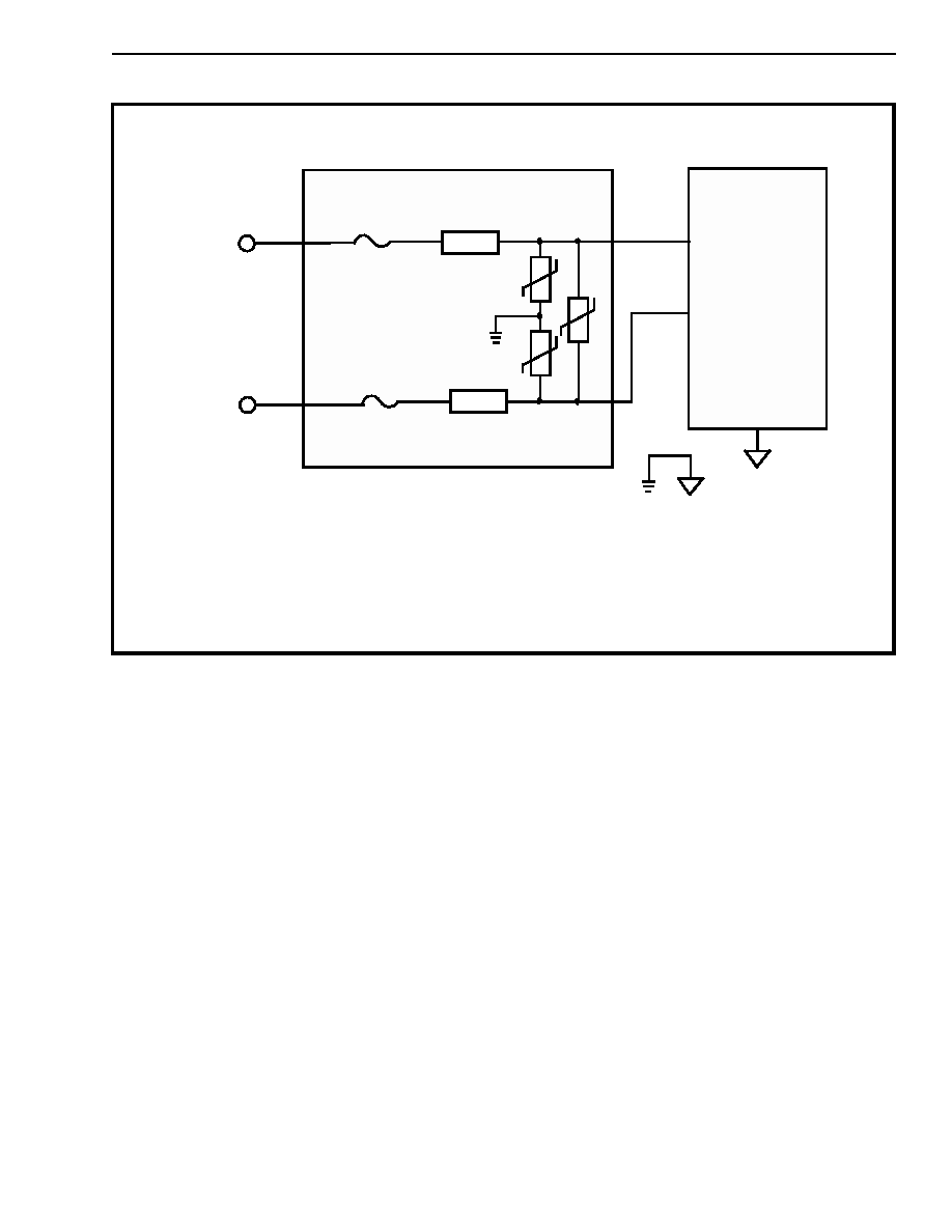
To meet the regulatory high voltage requirements, an
external protection circuit is required. The protection
circuit shown in Figure 9 is matched to the MH88632
and ensures than they meet the high voltage
requirements of FCC, DOC, CSA and UL when
installed in a properly designed system.
Products are designed in accordance with meeting
the above requirements; however, full conformance
to these standards is dependent upon the application
in which the hybrid is being used, and therefore,
approvals are the responsibility of the customer and
Mitel will not have tested the product to meet the
above standards.
DC Loop Termination
The DC loop termination circuitry provides the loop
with an active Dc load termination when a logic low is
applied to the LRC (Loop Start Relay Control) input.
the termination is similar to a DC resistance between
200
and 275
. An external relay is used to activate
internal circuitry which switches the termination in
and out of the loop. This is used for both seizing the
line as well as generating dial pulses.
Supervision Features
The supervision circuitry provides the signalling
status outputs. The system controlling the COIC,
monitors these logic outputs. The supervision
circuitry is capable of detecting ringing voltage, both
forward and reverse loop battery and loop current,
and both grounded tip lead and grounded ring lead.
a) Supervision Features RV (Ring Voltage
Detect Output)
The RV (Ringing Voltage Detect) output provides a
logic low when ringing voltage is detected. This
detector includes a ringing filter which ensures that
the output toggles at the ringing cadence and not at
the ringing frequency. Typically, this output goes low
50ms after ringing voltage is applied and remains
low for 50ms after ringing voltage is removed.
b) Supervision Features FL & RL (Forward Loop
and Reverse Loop Detect Output).
The FL (Forward Loop Detect) output provides a logic
low when either forward loop battery or forward loop
current is detected (ring lead voltage negative with
respect to ring lead). The RL (Reverse Loop Detect)
output provides a logic low when either reverse loop
battery or reverse loop current is detected (tip lead
voltage negative with respect to ring lead).
See Table 5 for Loop Battery and Current Status
Outputs.

Preliminary Information
MH88632
2-239
c) Supervision Features TG & RG (Tip Ground
and Ring Ground Detect Output)
The TG (Tip Lead Ground Detect) output provides a
logic low when the tip lead is at ground (AGND)
potential. The RG (Ring Lead Ground Detect) output
provides a logic low when the Ring lead is at ground
(AGND) potential.
See Table 6 for Loop Ground Status Outputs.
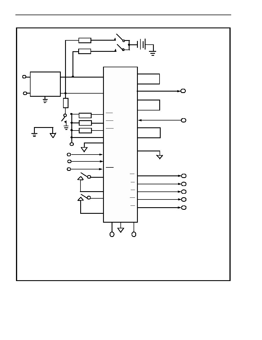
Ground Start Signalling Features
For Ground Start signalling, relay K2 and resistors
R1 and R2, and relay K3 and resistor R3 are
required (See Figure 8). Activation of K2 is controlled
by the logic signal at the BRC (Bias Relay Control)
input while activation of K3 is controlled by the logic
signal at the GRC (Ground Relay Control) input.
K2 is used to engage the bias resistors while K3 is
used to ground the right lead; this is used in ground
start applications for signalling to the central office.
Typical Ground Start Signalling
Protocol
Refer to Figure 8 for Typical LS-GS Application
Circuit.
In the idle state, the system (e.g., PBX control card)
provides a logic high to the BRC input. This activates
the COIC's second internal relay driver which
activates relay K2. Both contacts of relay K2 close,
which connect the -48VDC supply to Tip (tip lead)
and Ring (ring lead) through bias resistors R1 and
R2.
Depending on which Ground Start protocol is used,
initiating a Ground start call to the central office can
be performed by the following sequence of events.
The system provides a logic low to the GRC input.
this activates the COIC's third internal relay driver
which activates relay K3. The contacts of relay K3
close, which connects the ring lead to ground
through a current limiting resistor R3.
The Central Office reconizes the ring ground
condition and responds by grounding the tip lead.
The COIC senses the grounded Tip and switched the
TG (Tip Lead Ground Detect) output to a logic low.
The system then applies a logic high to the LRC
(Loop Relay Control) input. This activates the COIC's
first internal relay driver which activates relay K1.
Both contacts the relay K1 close, which activates the
COIC's internal circuitry resulting in an active line
termination across Tip and Ring. The system then
provides a logic low to the BRC input. This
deactivates the COIC's second internal relay driver
which deactivates K2. Both contacts of relay K2
open, which disconnect the bias from Tip and Ring.
The system then provides a logic high to the GRC
input. This deactivates the COIC's third internal relay
driver which deactivates relay K3. The contact of
relay K3 opens. which disconnects the grounded ring
lead. The voice link is now established.
Receiving a Ground Start call from central office is
performed similarly. The central office can signal the
COIC by either grounding the tip lead or by
grounding the ring lead.
Hybrid
The 2-4 Wire Hybrid circuit separates the balanced
full duplex signal at Tip and Ring of the telephone
line into receive and transmit ground referenced
signals at Rx (Receive) and TX (Transmit) of the
COIC. The hybrid also prevents the input signal at
RX from appearing at TX. The degree to which the
Hybrid minimises the contribution of the RX signal at
the TX output is specified as transhybrid loss. For
maximizing transhybrid loss, see the Network
Balance section.
The 4-Wire side can be interfaced to a filter/codec
such as the Mitel MT896X, for use in digital voice
switched systems.
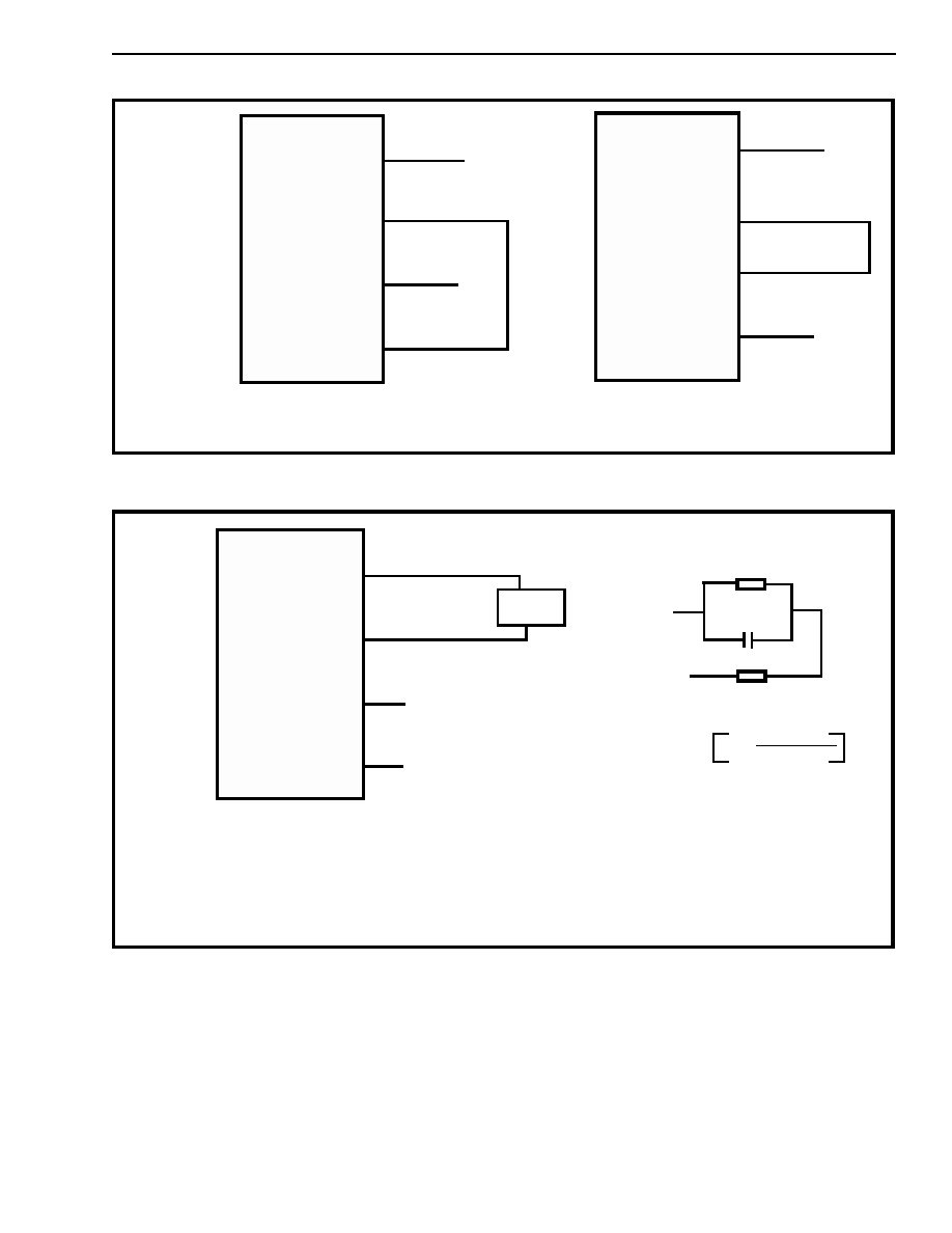
Line Impedance
The MH88632's Tip-Ring impedance (Z
in
) can be set
to 600
, 900
or to a user selectable value. Thus,
Zin can be set to any international requirements. The
connection to Z1 determines the input impedance.
With Z1 connected to Z600, the line impedance is set
to 600
.
With Z1 connected to Z900, the line
impedance is set to 900
. A user defined impedance
can be selected which is 0.1 times the impedance
between Z1 and Z2. For example, with 2200
in
series with 11.5nF in parallel with 8200
, all between
Z1 and Z2, the devices line impedance will be 220
in series with 115nF in parallel with 820
. See Table
3 and Figures 4 & 5.

MH88632
Preliminary Information
2-240
Stability
The part will be stable with an AC load over the
range 0.5 Z
in
<Load < 2 x Z
in
.
The range of loads that can be simulated by the
MH88632 is extensive including those which are
purely resistive and complex in nature. For loads
with a low or zero series resistance additional
measures need to be taken to maintain stability
which involves simulating with a larger series
resistance and adjusting other components
accordingly.
Examples:
Sweden
: Load is 900
in a parallel with 30nF. This
is synthesised on the MH88632 by 1.5k
in series
with a parallel combination of 3nF and 7.4k
.
Norway
: Load is 120
in series with a parallel
combination of 820
and 110nF. This is synthesized
on the MH88632 by 1.5k
in series with a parallel
combination of 12nF and 7.8k
.
Italy:
Load is 750
in parallel with 18nF. This is
synthesised on the MH88632 by 1.5k
in series with
a parallel combination of 2nF and 6k
.
Network Balance
Transhybrid loss is maximized when the line
termination impedance and COIC network balance
are matched. The MH88632's network balance
impedance can be set to Z
in
, AT&T (350
+1k
//
210nf) or to a user Selectable value. Thus, the
network balance impedance can be set to any
international requirement. A logic level control input
NS selects the balance mode. With NS at logic low,
an internal network balance impedance is matched
to the line impedance (Z
in
). With NS at logic high, a
user defined network balance impedance is selected
which is 0.1 times the impedance between N1 and
AGND. For example, with 2200
in series with
11.5nF in parallel with 8200
, all between N1and
AGND, and NS at logic high, the devices network
balance impedance in 220
in series with 115nF in
parallel with 820
, the impedance between N1 and
N2 must be equivalent to 10 times the input
impedance (Z
in
). In addition, with NS at logic high, an
AT&T network balance impedance can be selected
by connecting NATT to N1; in this case, no additional
network is required between N1 and N2. See
Table 4 and Figures 6 & 7.
TIP-RING Drive Circuit
The audio input ground referenced signal at RX is
converted to a balanced output signal at Tip and
Ring. The Tip-Ring Drive Circuit is optimised for
good 2-Wire longitudinal balance.
TIP-RING Receive Circuit
The differential audio signal at Tip and Ring is
converted to a ground referenced audio signal at the
TX output. This circuit operates with or without loop
current; signal reception with no loop current is
required for on-hook reception enabling the detection
of ANI (Automatic Number Identification) signals.
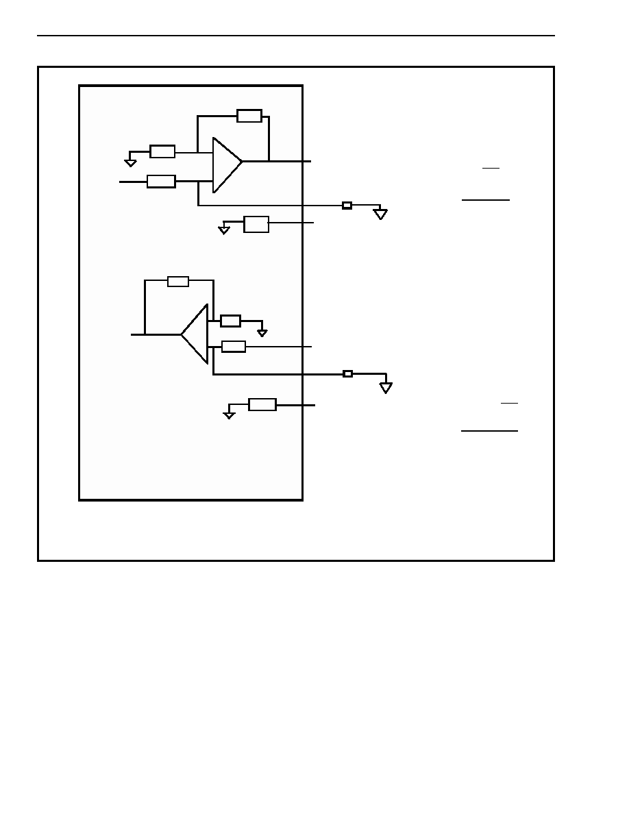
Programmable Transmit and Receive
Gain
Transmit gain (Tip-Ring to TX) and receive Gain (RX
to Tip-Ring) are programmed by connecting external
resistors (RRX and RTX) from GRX1 to AGND and
from GTX1 to AGND as indicated in Figure 3 and
Tables 1 and 2. The programmable gain range is
from -12dB to +6dB; this wide range will
accommodate any loss plan. Alternatively, the
default Receive Gain of 0dB and Transmit Gain of
0dB can be obtained by connecting GRX0 to GRX1
and GTX0 to GTX1. In addition, a Receive Gain of
+6dB and Transmit Gain of +6dB can be obtained by
not connecting resistors RRX and RTX. For correct
gain programming, the MH88632's Tip-Ring
impedance (Z
in
) must match the line termination
impedance. For optimum performance, resistor RRX
should be physically located as close as possible to
the GRX1 input pin.
ANI (Automatic Number Identification)
ANI provides the called party with calling party
telephone number identification. The central office
utilizes the voice path of a regular loop-start
telephone line when the COIC (subscriber's terminal)
is in the on-hook state. The central office sends the
ANI information (data transmission typically of an
FSK signal of 1200Hz and 2200Hz) typically 600ms
after the first ringing burst.
The COIC outputs this FSK signal at the TX output.
2-241
Preliminary Information
MH88632
Absolute Maximum Ratings
*
* Exceeding these values may cause permanent damage. Functional operation under these conditions is not implied.
Recommended Operating Conditions
* Typical figures are at 25
∞
C with nominal
+
5V supplies for design aid only.
DC Electrical Characteristics
DC Electrical Characteristics are over recommended operating conditions unless otherwise stated.
* Typical figures are at 25
∞
C with nominal +5V supplies and are for design aid only.
Loop Electrical Characteristics
Parameter
Sym
Min
Max
Units
1
DC Supply Voltage
V
DD
V
EE
-0.3
0.3
7
-7
V
V
2
DC Ring Relay Voltage
V
RLY
-0.3
20
V
3
Storage Temperature
T
S
-55
+125
∞
C
Parameter
Sym
Typ*
Min
Max
Units
Comments
1
DC Supply Voltage
V
DD
V
EE
5.0
-5.0
4.75
-4.75
5.25
-5.25
V
V
2
DC Ring Relay Voltage
V
VRLY
5.0
15
V
3
Operating Temperature
T
OP
0
70
∞
C
Characteristics
Sym
Min
Typ*
Max
Units
Test Conditions
1
Supply Current
I
DD
I
EE
13
13
mA
mA
2
Power Consumption
PC
137
mW
3
FL
RL
RG
TG
RV
Low Level Output Voltage
High Level Output Voltage
V
OL
V
OH
2.4
0.5
V
V
I
OL
= 4mA
I
OH
= 0.5mA
4
LRD
BRD
GRD
Sink Current, Relay to V
DD
Clamp Diode Current
I
OL
I
CD
100
510
mA
mA
V
OL
= -.35V
5
NS
LRC
BRC
GRC
Low Level Input Voltage
High Level Input Voltage
V
IL
V
IH
2.0
0.8
V
V
6
High Level Input Current
Low Level Input Current
I
IH
I
IL
1
1
µ
A
µ
A
Characteristics
Sym
Min
Typ*
Max
Units
Test Conditions
1
Ringing Voltage
VR
40
90
130
Vrms
2
Ringing Frequency
17
20
33
Hz
3
Ringer Equivalent Number
REN
3
(Type A)
4
Operating Loop Current
18
mA
5
Operating Loop Resistance
0
90
@18mA, -48V
6
Off-Hook DC Resistance
2300
7
Leakage Current
(Tip-Ring to AGND)
10
mA
@1000Vac
8
FL Threshold
Tip-Ring Voltage Detect
Tip-Ring Current Detect
+30
+1.0
+40
+4.2
Vdc
Vdc
LRC-0V
LRC=0V
2-242
MH88632
Preliminary Information
Loop Electrical Characteristics (Continued)
DC Electrical Characteristics are over recommended operating conditions unless otherwise stated.
* Typical figures are at 25
∞
C with nominal
+
5V supplies and are for design aid only.
Characteristics
Sym
Min
Typ*
Max
Units
Test Conditions
9
RL Threshold
Tip-Ring Voltage Detect
Tip-Ring Current Detect
-30
-1.0
-40
-40
Vdc
Vdc
LRC = 0v
LRC = 0V
10
TG and RG Detect Threshold
-12
-14
Vdc
AC Electrical Characteristics
Characteristics
Sym
Min
Typ*
Max
Units
Test Conditions
1
2-wire Input Impedance
x
Z
in
600
900
Ext.
2
Return Loss at 2-Wire
(Z
in
= Ref. = 600
)
RL
20
20
20
dB
dB
dB
200-500 Hz
500-1000 Hz
1000-3400 Hz
3
Return Loss at 2-Wire
(Z
in
= Ref. = 900
)
RL
20
20
20
dB
dB
dB
200-500 Hz
500-1000 Hz
1000-3400 Hz
4
Return Loss at 2-Wire
y
(Z
in
= Ref. = External)
RL
20
20
20
dB
dB
dB
200-500 Hz
500-1000 Hz
1000-3400 Hz
5
Longitudinal to Metallic Balance
y z {
58
58
55
53
51
dB
dB
dB
dB
dB
200 Hz
1000 Hz
2000 Hz
3000 Hz
4000 Hz
6
Metallic to Longitudinal Balance
60
40
dB
dB
200-1000 Hz
1000 -4000 Hz
7
Transhybrid Loss
(Z
in
= Ref. = Net = 600
)
THL
18
21
dB
dB
200-3400 Hz
500-2500 Hz
8
Transhybrid Loss
(Z
in
= Ref. = Net = 900
)
THL
18
21
dB
dB
200-3400 Hz
500 -2500 Hz
9
Transhybrid Loss
(Z
in
= Ref. = Net = External)
THL
18
21
dB
dB
200-3400 Hz
500-2500 Hz
10
Transhybrid Loss
(Z
in
= Ref. = Net = 600
)
THL
18
21
dB
dB
200-3400 Hz
500-2500 Hz
11
Input Impedance At RX
k
12
Output Impedance at TX
13
Transmit Gain, (TX/2-Wire):
Default Gain (0dB)
y z
Programmable Range
Frequency response gain
y z
(relative to gain at 1kHz)
dB
dB
dB
dB
dB
dB
Input 0.5V
1kHz
1kHz
200 Hz
300 Hz
3000 Hz
3400 Hz
14
Receive Gain, (2-Wire/RX):
Default Gain (0dB)
y z
Programmable Range
Frequency response gain
y z
(relative to gain at 1kHz)
dB
dB
dB
dB
dB
dB
Input 0.5V
1kHz
1kHz
200 Hz
300 Hz
3000 Hz
3400 Hz
2-243
Preliminary Information
MH88632
* Typical figure are at 25
∞
C with nominal +5V supplies and are for design aid only.
AC Electrical Characteristics are over recommended operating conditions unless otherwise stated.
x
Impedance set by external network of 600
or 900
default.
y
External network for test purposes consists of 2200
+ 8200
// 11.5nF between pins Z1 and Z2, the equivalent Zin has 1/10
th
the impedance
and is equivalent o 220
+820
// 115nF
z
Test condition uses a Z
in
value of 600
, 900
and the above external network.
{
Test conditions use a transmit and receive gain set to 0dB default and a Z
in
value of 600
unless otherwise stated.
Notes:
Test conditions use a transmit and receive gain set to 0dB default and a Z
in
value of 600W unless otherwise stated.
Test conditions uses both the off-hook state (LRC=+5VDC) and the on-hook state (LRC=AGND)
"Ref" indicates reference impedance which is equivalent to the termination impedance.
"Net" indicates network balance impedance
Tables 1 & 2: Transmit and Receive Gain Programming
Note 1: See Figures 3 and 4 for additional details.
Note 2: Overall gain refers to the receive path of PCM to 2-wire, and transmit path of 2-wire to PCM.
15
Signal Output Overload Level
at 2-wire
at TX
4.0
4.0
dBm
dBm
% THD< 5%
Ref. 600
Ref. 600
16
Total Harmonic Distortion
at 2-Wire
at TX
THD
1.0
1.0
%
%
Input 0.5V, 1kHz
17
Idle Channel Noise
at 2-Wire
at Tx
Nc
13
13
dBrnC
dBrnC
18
Power Supply Rejection Ratio
at 2-Wire and TX
V
DD
V
EE
PSRR
20
20
30
30
dB
dB
Ripple 0.1V, 1kHz
19
On-Hook Transmit Gain,
(TX/2-Wire)
Default Gain (0dB
Programmable Range
On-Hook frequency Response
Gain (relative to gain to 1kHz)
-1
-12
-3
-1
1
6
1
1
dB
dB
dB
dB
Input 0.5V
1kHz
1kHz
200 Hz
3400 Hz
Transmit
Gain (dB)
RTX Resistor
Value (
)
Notes
+6.0
No Resistor
+4.0
38.3k
Results in 0dB overall gain when used with Mitel A-law codec (i.e. MT8965)
+3.7
32.4k
Results in 0dB overall gain when used with Mitel
µ
-law codec (i.e. MT8964)
0.0
GTX0 to GTX1
-3.0
5.49k
-6.0
3.32k
-12.0
1.43k
Receive Gain
(dB)
RRX Resistor
Value (
)
Notes
+6.0
No Resistor
0.0
GRX0 to GRX1
-3.0
5.49k
-3.7
4.87k
Results in 0dB overall gain when used with Mitel A-law codec (i.e. MT8965)
-4.0
4.64k
Results in 0dB overall gain when used with Mitel
µ
-law codec (i.e. MT8964)
-6.0
3.32k
-12.0
1.43k
AC Electrical Characteristics
(Continued)
Characteristics
Sym
Min
Typ*
Max
Units
Test Conditions
2-244
MH88632
Preliminary Information
Figure 3 - Gain Programming with External Components
MH88632
Z
Z
10k
10k
Z
10k
10k
GRX0
GRX1
GTX0
GTX1
RX
RRX
RTX
TX
TRANSMIT GAIN
:
(Tip-Ring to Tx)
AV= -20log (0.5+5k
)
RTX
RTX = 5k
Example
RTX = 38k
; AV = +4dB
RECEIVE GAIN:
(RX to Tip-Ring)
AV= -20log (0.5 + 5k
)
RRX
RRX = 5k
Example:
RRX = 4.6k
; AV = -4dB
25
28
27
26
30
29
+
-
+
-
Z
10
(-AV/20)
-0.5
10
(-AV/20)
-0.5
2-245
Preliminary Information
MH88632
Figure 4 - Input Impedance (Z
in
) Settings with Z
in
equal to 600 or 900
Figure 5 - Input Impedance (Z
in
) Settings with Z
in
not equal to 600 to 900
24
23
22
32
24
23
22
32
NC
NC
NC
NC
MH88632
MH88632
Z900
Z600
Z900
Z600
Z1
Z2
Z1
Z2
Input impedance (Z
in
) set to 600
Input Impedance (Z
in
) set to 900
Note: Make connection between Z1 and other points as short as possible
24
23
22
32
MH88632
Z900
Z600
Z1
Z2
Notes:
1) The 10xZ
in
network must be set to 10 x the desired input impedance (Z
in
).
2) The network balance must be set to the desired network balance. (See
section on network balance.)
3) Make connection between Z1 and component as short as possible.
RS+
1/RP + S x CP
where S = j x w
and w = 2 x
x f
Example:
If RS = 2200
, RP = 8200
, CP= 11.5nf
Then the input impedance (Z
in
) is 220
in
series with 820
in parallel with 115nF.
10 x Z
in
RP
Z1
Z2
CP
RS
Z
in
= 0.1 x
1
2-246
MH88632
Preliminary Information
Figure 6 - Network Balance Setting with NETBAL equal to Z
in
or AT&T
Figure 7 - Network Balance Setting with NETBAL not equal to Z
in
or AT&T
21
20
19
33
21
20
19
33
VDD
MH88632
MH88632
NATT
NS
NATT
NS
N1
N2
N1
N2
Network balance is set to the input
Network balance is set to the AT&T compromise
Note: Make connection between Z1 and other points as short as possible
Impedance (Z
in
)
network (350
+ 1000
// 210nF)
impedance. The input impedance must be
set to 600
.
21
20
19
33
MH88632
NATT
NS
N1
N2
Notes
:
1) The 10xZ
in
network must be set to 10 x the desired input impedance (Z
in
)
.
2) The network balance must be set to the desired network balance. See
section on network balance.
3) Make connection between Z1 and component as short as possible.
Example:
If RS = 2200
,
RP = 8200
, CP= 11.5nf
Then the input impedance (ZNetbal) is 220
in
series with 820
in parallel with 115nF.
VDD
RP
N2
N1
CP
RS
10 x Z
in
10 x NETBAL
ZNetbal = 0.1 x
1/RP + (S x CP)
where S = j x w
and w = 2 x
x f
RS +
1
2-247
Preliminary Information
MH88632
Table 3: Input Impedance Settings
Note 1: NA indicates high impedance (10k
) connection to this pin does not effect the resulting network balance.
Note 2: See Figure 4 & 5 for Applications Circuits
Table 4: Network Balance Settings
.
Note 1: NA indicates high impedance (10k
) connection to this pin does not effect the resulting network balance.
Note 2:Low indicates Logic Low.
Note 3: See Figures 6 and 7 for Application Circuit.
Table 5: Control Decode Table
Note 1: VT - VR = Differential voltage from Tip to Ring VR - VT = Differential voltage from Ring to Tip
Note 2: Low indicates Logic Low. High indicates logic High.
Note 3: See Figures 8 & 10 for Application Circuit.
Table 6: Loop Current Setting
Note 1: VT - VR = Differential voltage from Tip to Ring VR - VT = Differential voltage from Ring to AGND
Note 2: A > -B indicates that "A" is less negative than "-B". A<-B indicates that "A" is more negative than "-B".
Note 3:Low indicates Logic Low. High indicates logic High.
Note 4: See Figure 8 for Application Circuit.
Z2
Z1
Z600
Z900
Resulting input impedance (Z
in
)
NA
Connect Z1 to Z600
NA
600
NA
Connect Z1
to Z9000
NA
Connect Z1
to Z900
900
Connect network from Z1 to Z2
NA
NA
0.1 x impedance between Z1 & Z2
NS (Input)
N2
N1
NATT
Resulting input impedance (Z
in
)
Low
NA
NA NA
Equivalent
to
Z
in
High
NA
Connect N1 to NATT
AT&T compromise (350
+ 1k
// 210nF)
Zin must be 600
High
Connect network from N1 to
AGND equivalent to 10 x
NETBAL. Connect network
from N1 to N2 equivalent to 10
x Z
in
.
NA
0.1 x impedance between N1 & N2
Loop Status
Loop Condition
LRC (Input)
FL (Output)
RL (Output)
Forward Battery
VT-VR > 40 V
Low
Low
High
Forward Current
VT-VR > 3.4 V
High
Low
High
Reverse Battery
VR-VT > 40V
Low
High
Low
Forward Current
VR-VT > 3.4 V
High
High
Low
No Battery
IVT-VRI > 1.0 V
Low
High
High
No Current
IVT-VRI > 10 V
High
High
High
Not Valid
No Condition
High or Low
Low
Low
Loop Status
Loop Condition
RG (Output)
TG (Output)
Ring and Tip open
VT-VG > -14 V
VR-VG < -14V
High
High
Ring Ground and Tip
Open
VR-VG > -12 V
VT-VG < -14V
Low
High
Tip Ground and Ring
Open
VT-VG > -12 V
VR-VG < -14V
High
Low
Ring and Tip Ground
VR-VG > -12 V
VT-VG < -12V
Low
Low
2-248
MH88632
Preliminary Information
Loop Current Setting
Figure 8 - Typical LS-GS Application Circuit
MH88632
NS
RGND
PROTECTION
CIRCUIT
K1
K2
K3
R3
R1
R2
48V BATTERY
LOOP RELAY CONTROL
BIAS RELAY CONTROL
GROUND RELAY CONTROL
AUDIO OUT
AUDIO IN
RING DETECT
FORWARD LOOP
REVERSE LOOP
RING GROUND
RING DETECT
GTX1
GTX0
TX
GRX1
GRX0
RX
Z1
Z600
NS
RV
FL
RL
RG
TG
VEE
AGND
VDD
XLD
XLC
XLB
XLA
GRC
BRC
LRC
RGND
VRLY
GRD
BRD
LRD
RING
TIP
TIP
RING
K3
+5V
-5V
28
27
25
30
29
26
23
32
33
36
37
35
38
34
39
18
40
6
5
4
3
17
16
15
11
12
8
14
13
2
1
NOTES:
1) SEE FIGURE 9 FOR PROTECTION CIRCUIT
2) CONFIGURED FOR 0dB GAIN, 600
ZIN AND BALANCE
3) K1, 2 E/M FORM C
4) K3 E/M 1 FORM C
5) R1, R2 30.9k
, 1%, 5W
6) R3 470
, 5%, 5W
7) K2, 3, R1, 2, 3 REQUIRED FOR GS ONLY
K2A
K2B
K1A
K1B
2-249
Preliminary Information
MH88632
Figure 9 - External Protection Applications Circuit
MH88632
R1
F1
F2
R2
Notes:
1) F1, 2 1AMP, 250VAC, SLOW-BLOW LITTLEFUSE 230 2AG
2) R1, 2, 2.4
5% 1/2W 350V, FLAME RATED RESISTOR i.e, ALLEN BRADLEY EB24G5, DALE/VISHAY LCA 0411NE 2.4
5%
3) RV1, 2, 3, 250VAC, 35J, METAL OXIDE VARISTOR i.e., HARRIS, V250LA10, OHIZUMI 0250NC12D
PROTECTION CIRCUITRY
RV1
RV2
RV3
TIP
RING
TIP
RING
AGND
1
2
18
2-250
MH88632
Preliminary Information
Figure 10 - Typical LS Application Circuit
MH88632
PROTECTION
CIRCUIT
K1
LOOP RELAY CONTROL
AUDIO OUT
AUDIO IN
RING DETECT
FORWARD LOOP
REVERSE LOOP
GTX1
GTX0
TX
GRX1
GRX0
RX
Z1
Z600
NS
RV
FL
RL
VEE
AGND
VDD
XLD
XLC
XLB
XLA
GRC
BRC
LRC
RGND
VRLY
LRD
RING
TIP
TIP
RING
+5V
-5V
28
27
25
30
29
26
23
32
33
36
37
35
39
18
40
6
5
4
3
17
16
15
11
12
13
2
1
NOTES:
1) SEE FIGURE 9 FOR PROTECTION CIRCUIT
2) CONFIGURED FOR 0dB GAIN, 600
ZIN AND BALANCE
3) K1, E/M 2 FORM C
K1
K1
2-251
Preliminary Information
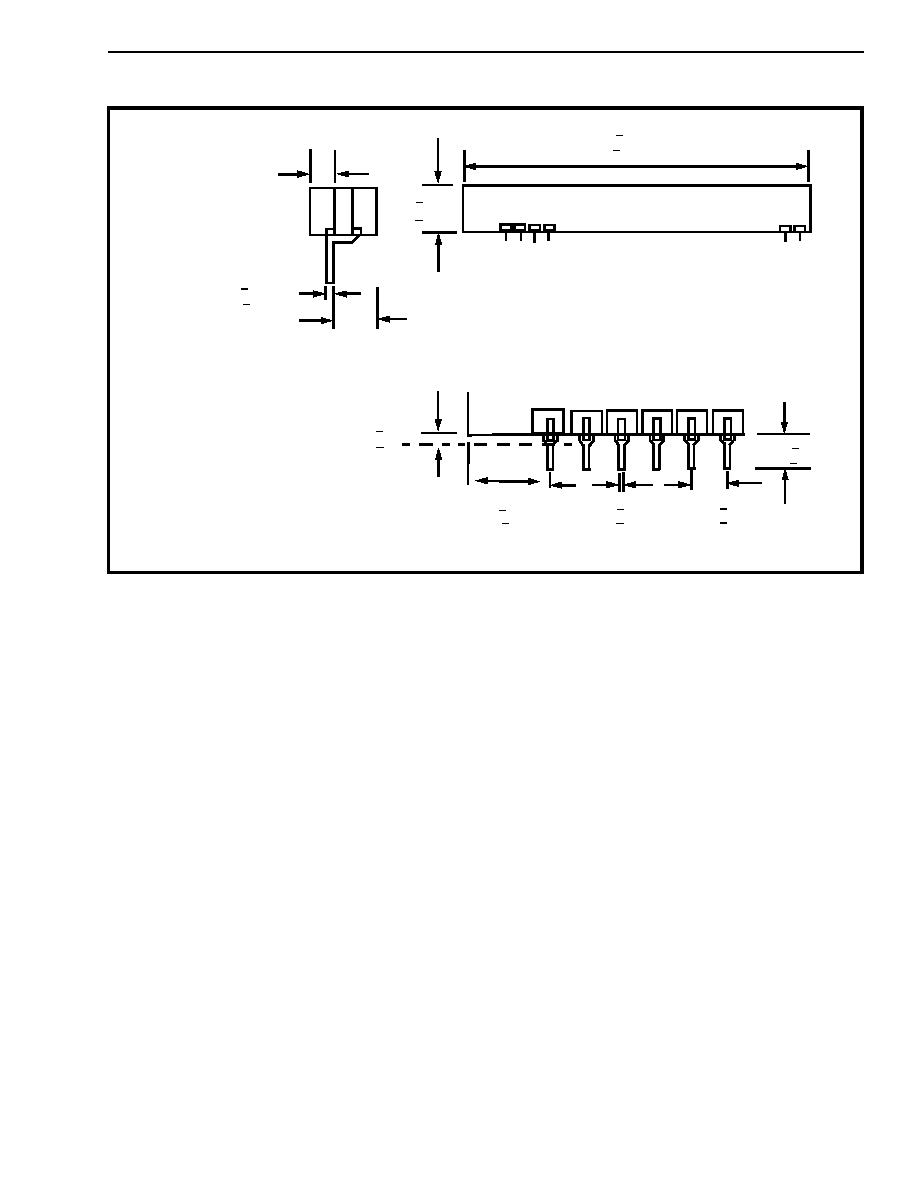
MH88632
Figure 11 - Mechanical Data
4.20 + 0.020
(107 + 1.0)
0.58+0.02
(14.7+0.5)
0.12 Max
(3.1 Max)
0.010 + 0.002
(0.25 + 0.05)
0.080 Max
(2.0 Max)
Side View
0.05 + 0.01
(1.3 + 0.5)
*
*
*
0.25 + 0.02
(1.3 + 0.05)
0.020 + 0.05
(0.51 + 0.13)
0.100 + 0.10
(2.54 + 0.13)
0.18 + 0.02
(4.6 + 0.5)
39 40
4
Notes:
1) Not to scale
2) Dimensions in inches).
3) (Dimensions in millimetres).
*Dimensions to centre of pin &
tolerance non accumulative.
1 2 3

2-252
MH88632
Preliminary Information
Notes: